
 Open Access Article
 This Open Access Article is licensed under a
 Creative Commons Attribution 3.0 Unported Licence
Photoluminescence and lasing characteristics of single nonpolar GaN microwires
S. S. Yana,
A. Q. Chenb,
Y. Y. Wuc,
H. Zhuc,
X. H. Wangd,
C. C. Lingb and
S. C. Su *ab
*ab
aGuangdong Provincial Key Laboratory of Nanophotonic Functional Materials and Devices, Institute of Opto-electronic Materials and Technology, South China Normal University, Guangzhou 510631, China. E-mail: shichensu@scnu.edu.cn
bDepartment of Physics, The University of Hong Kong, Hong Kong, China
cState Key Laboratory of Optoelectronic Materials and Technologies, School of Physics, Sun Yat-Sen University, Guangzhou 510275, China
dInstitute of Microelectronics, Tsinghua University, Beijing 100084, China
First published on 18th April 2017
Abstract
Nonpolar a-axial GaN MWs were fabricated on a patterned Si substrate via metal–organic chemical vapor deposition (MOCVD) without the assistance of any catalyst. The temperature-dependent photoluminescence (PL) properties of a single GaN MW were discussed comprehensively. Below the temperature of 90 K, the neutral donor-bound exciton (D0X) line dominates in the spectrum, while the free–exciton transition dominates at temperatures above 90 K. The optical properties of GaN MWs exhibit a multiple-mode-stimulated-amplified emission with a peak around 375 nm and a corresponding lasing threshold of about 120 kW cm−2. In addition, the lasing characteristics of GaN MWs were explored by the finite-difference time-domain (FDTD) method.
Introduction
Over the last decade, III-nitride semiconductor materials have attracted extensive attention in optical and electrical devices due to their superior properties.1,2 Gallium nitride (GaN) has a wide direct band gap of 3.4 eV in the ultraviolet (UV) region, is stable at high temperature, and is applicable in high power electronics.3 In addition, GaN also possesses large exciton binding energy and fast saturation speed of electronic drift, so that GaN has plenty of applications in nanolasers,4 field-effect transistors,5 light-emitting diodes,6,7 electric generators,8,9 field emitters,10,11 and UV photosensors.12 Low-dimensional structures such as GaN microwires (MWs) are expected to offer potential advantages for micro–nano photonics and micro–nano electronics due to their non-planar geometry, high crystalline quality, superior optical gain property and higher compatibility with the well-established silicon technology.13 The single crystalline GaN MW has been considered as one of the most promising materials for detecting UV spectrum because of its direct and suitable wide band gap and high absorption coefficient in the UV range.14 Optical properties of GaN MWs have been extensively studied, including reflectance and transmission in the UV-visible-infrared region,15,16 photoluminescence (PL),17–20 and Raman scattering spectroscopy.17,21–23 The quantum confinement effect responsible for direct band-to-band transition in the encapsulated one-dimensional MW has been observed.18 Remarkably, the lasing of nonpolar GaN MW grown on (100) γ-LiAlO2 single crystal substrate was firstly demonstrated over the past decade.24 However, great efforts still remain to be made in order to precisely discuss the optical properties of nonpolar GaN MWs. In addition, single MW has been made to act as optical wave-guides and Fabry–Perot cavities.25However, there are few reports about the nonpolar GaN MWs fabrication and optical properties. Since the polarizations of nitrides depend on the composition and the strain state, the polarization discontinuities exist at the device interfaces. These polarization changes are related to the fixed charge that produces the internal electric field, which will reduce the oscillator strength and cause a red shift of the optical transition.26,27 As a result, the nonpolar a-axial GaN MW provides a solution of eliminating polarization-induced electric field effects in nitride quantum structures. The correlational research of nonpolar GaN MW needs to be further studied.
In this work, the nonpolar GaN MWs were fabricated and the optical properties of GaN MWs were discussed in details. The neural donor-bound exciton (D0X) and the free-exciton (FX) transition dominate in the spectrum at low and high-temperature, respectively. The excellence optical properties of GaN MWs have been illustrated comprehensively, especially for the stimulated amplified emission. In addition, lasing characteristics of GaN MWs were also explored by the finite-difference time-domain (FDTD) method.
Experimental section
Materials and synthesis
For obtaining the single nonpolar α-axial GaN MW, firstly, highly ordered nonpolar a-axial GaN MWs were grown on patterned Si substrate via metal–organic chemical vapor deposition (MOCVD) without the assistance of any catalyst, then the single GaN MW was released by selective wet etching and ultrasonic process.Measurements
All the experiments were carried out in LabRAM HR Evolution system. In order to measure the PL spectra, the MW was mounted on the closed cycle cryostat with varying temperature from 80 K to 300 K, and excited by the He–Cd laser (325 nm). With regard to the lasing characteristics, the Q-switch Nd:YAG laser (266 nm) at pulsed operation (6 ns, 30 Hz) was utilized. A monochromator (Princeton instrument) was used to analyze the stimulated emission from the edge of single GaN MW collected by an ultraviolet objective lens at room temperature.Results and discussion
Highly ordered nonpolar a-axial GaN MWs in our experiments were grown on patterned silicon (100) substrate via metal–organic chemical vapor deposition (MOCVD) technique without the assistance of catalyst.28 The dimension and chemical composition of MWs can be controlled precisely and efficiently by adjusting the pattern of the silicon substrate and tuning of the growth parameters. Two semi-polar crystallographic planes that formed during the growth of the GaN core can be utilized as growth templates for multiple quantum wells or device structure, which will reduce the piezoelectric fields in the active regions. Fig. 1a shows the schematic illustration of the prepared patterned Si substrate. The trapezoidal grooves along the 〈−110〉 axis of the Si substrate are vertically truncated. Two opposite Si(111) facets of the trapezoidal grooves are separated by a bottom of Si (100) facet. The GaN MWs were synthesized on the sidewall of Si(111) facets selectively and the length of the MWs can be controlled by adjusting the length between adjacent ditches. Fig. 1b shows the optical microscopy images of the synthesized GaN MW arrays (redder line) in the plane of the patterned Si substrate. Fig. 1c shows the representative SEM image of the fabricated single GaN MW released from MW arrays on Si substrate by selective wet etching and ultrasonic process. The longitudinal direction of the as-grown GaN MW was a nonpolar 〈11−20〉 direction corresponding to the longitudinal direction of the trapezoidal groove array on the Si substrate.29 Fig. 1d shows the cross-side SEM image of a single GaN MW, and the GaN MW possesses a faced surface and is enclosed by three sidewalls, that is to say, the cross-section of the GaN MWs is triangle. Fig. 1e shows the complete morphology SEM image of single GaN MW. As shown in Fig. 1e, it is worth pointing out that the GaN MW used in these experiments has a diameter about 600 nm. In addition, the length was up to several hundreds of micrometers. The X-ray diffraction (XRD) patterns of the GaN MWs grown on Si substrate are shown in Fig. 1f. It can be observed that the diffraction angle of the peak is 68°, which is corresponding to the (112) facet (a-plane) of GaN MW, as shown in Fig. 1d, the cross section of the GaN MW is triangle. The reason that the MWs tend to exhibit triangle cross section rather than trapezoidal is the presence of the (0001) facet. For the reason that the elongated axis of the wires is 〈11−20〉, so the GaN MWs used in the experiment is nonpolar. Moreover, compared with the FWHM value of the peak 332 arcsec30 (0.0920), the narrower value as shown in Fig. 1f is only 0.0680, which reveal the GaN MWs synthesized has excellent crystalline quality.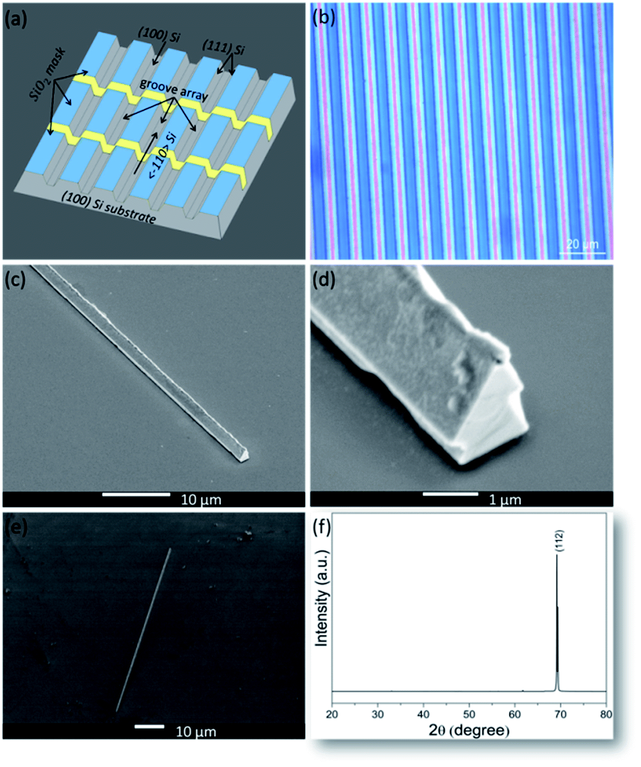 | ||
| Fig. 1 (a) Schematic illustration of the patterned Si substrate. (b) The optical microscopy images of GaN MWs (redder line) on the Si substrate. (c) The complete morphology SEM image of the single GaN MW. The single MW was released by selective wet etching and dispersed by ultrasonic process. (d) Enlarged SEM image of the NM that grown by MOCD. (e) Cross-section SEM image of single GaN-MW. (f) The X-ray diffraction pattern of the sample. | ||
The temperature-dependent PL spectra of the sample are shown in Fig. 2. Clearly, the neutral donor-bound exciton (D0X) line dominates in the examined low-temperature range (bellow 90 K). Its full width at half maximum is 2.6 meV under low power excitation, which indicates high quality of the sample. In strain-relaxed GaN sample (homoepitaxial films, or thick heteroepitaxial films), the D0X peak occurs at 3.471 eV at low temperature.31 In our GaN MW, the D0X peak occurs at 3.468 eV at 80 K, indicating the similarity of strain-relaxation. The FX transition is also well disintegrated. As temperature increased, the relative intensity of the FX line with respect to the D0X line rapidly increased. This is obviously due to the thermal decomposition of the bound exciton into the free exciton. However, D0X transition still keeps its dominant position in the given temperature range. The longitudinal optical (LO) phonon-assisted luminescence spectra measured at different temperature are also shown in this figure. It can be clearly observed that the emission band occurs at 3.387–3.397 eV. The origin of this band is the LO phonon replica of D0X (D0X–1LO). In addition, another peak occurred at 3.293–3.296 eV can be attributed to D0X-2LO.27 When the temperature increases gradually, the intensity of D0X becomes weaker and the peaks shift toward lower energy. At above 130 K, the D0X peaks are too weak to be identified and the free exciton peaks become dominant in the spectrum. In particular it should be noted that the free excitonic transition is traceable for the whole temperature range and no contribution from band-to-band transition has been noticed.
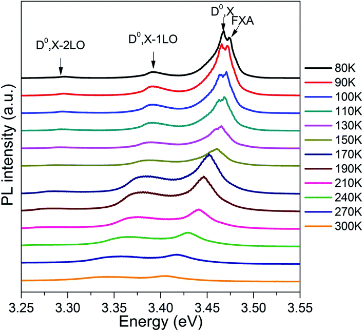 | ||
| Fig. 2 Temperature-dependent PL spectra of the GaN MWs from temperatures from 80 to 300 K. The emission spikes in the spectrum has been indicated. | ||
Fig. 3 shows the temperature dependence of the PL peak energies of FX and D0X emissions extracted from Fig. 2. In Fig. 3, it can be found that there is small energy difference between the free exciton and D0X emissions as the temperature is below 130 K, whereas donor-bound exciton has disappeared so that it cannot be resolved anymore for higher temperature. As expected, the energetic spacing between these transitions has no dependencies with temperature. The energetic different between FX and D0X is about 5.6 meV, which is in good agreement with the range thermal activation energy in the range of 5–7 meV (GaN film).32 The D0X gradually was quenched into FX with the temperature increasing.
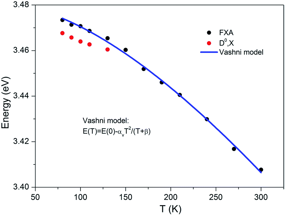 | ||
| Fig. 3 The peak energy of the two emission peaks of the GaN MWs as a function of the measured temperature. The solid line is the fitting curve according to the Vashni model. | ||
For most semiconductor, the variation of the band gap with temperature can be described by the semi-empirically found Vashni formula.33 Concerning the FX peaks shift towards lower energy with the increasing of the temperature, the band gap of the GaN MW (Eg) versus temperature has been fitted via Vashni model.34 The Vashni formula is given as follows:
 | (1) |
In order to explore the lasing characteristics of a single GaN MW, the single MW sample was studied by a Q-switch Nd:YAG laser (266 nm) at pulsed (6 ns, 30 Hz) operation. As shown in Fig. 4a, the image of GaN MWs with a triangular cross-section is excited by a 266 nm nanosecond-pulsed laser, which was taken by a digital camera. It can be observed that the blue-violet light emitted from the GaN MW of the two ends is brighter than the center of the GaN MW, which preliminarily indicates strong waveguide behavior and the axial cavity modes are Fabry–Perot (F–P) rather than whispering gallery modes (WGMs). Stimulated emission from the edge of single GaN MW was collected by an objective lens and analyzed by a monochromator (Princeton instrument) at room temperature. It can be seen that a relatively broad spontaneous emission band at 375 nm from the MW ends dominants in the spectrum at low excitation power of 100 kW cm−2 (Fig. 4b). With increasing excitation power, the end emission intensity increased rapidly and became dominant. Meanwhile, the peak intensity increase super-linearly with the pumping power and the line width of peak decrease dramatically. The above results indicate that the stimulated lasing was constructed in the single GaN MW. Since the single GaN MW used in the stimulated emission is nonpolar, which can remove polarization induced electric effects. Compared with polar GaN MW laser, nonpolar GaN MW laser is free from quantum confined Stark effect (QCSE). Fig. 4c shows the lasing threshold Pth extracted to be from the light-in to light-out curve. The threshold excitation power of the GaN MW is about 120 kW cm−2. It can also be observed that when the excitation power exceeds its threshold, this spontaneous emission peak collapsed into several well-defined narrow peaks centered at around 375 nm, thus indicating strong waveguide properties. It is worth to point out that the strongest laser mode occurred at 375 nm and the FWHM of this peak measured at the stimulated emission is less than 1 nm. This indicates that the mode in the MW cavity is longitudinal. In order to confirm the assumption, the following formula was used to calculated the mode spacing mode:36
 | (2) |
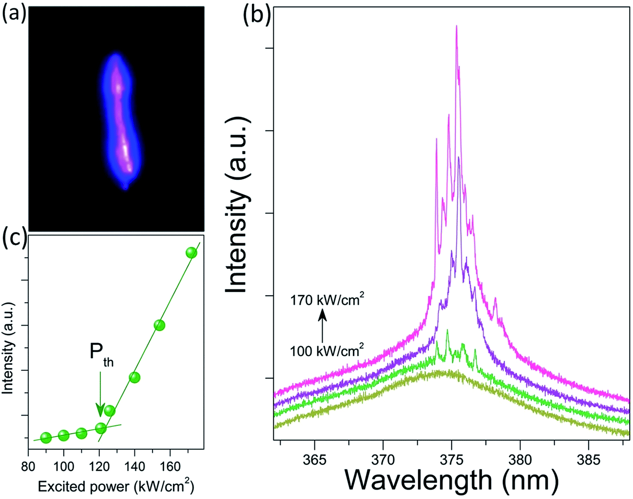 | ||
| Fig. 4 (a) The far-field image of the lasing a bare GaN MW which was taken by a digital camera. (b) Room-temperature lasing spectra of the single GaN MW with different excitation intensity. (c) Emission intensity versus excited power. The plot presents the evolution from a spontaneous emission, amplified spontaneous emission to lasing process. | ||
To further demonstrate the optical field confinement and light propagation along the wire related to different diameter, the two-dimensional (2D) finite-difference time-domain (FDTD) method (lumerical FDTD solutions) was used to perform the stimulated emission of the GaN MW.38 The FDTD method is a fully vectorial approach that naturally gives both the time domain and frequency domain information.39 Near field E(x,y) patterns of the trilateral cross section of GaN MW resonator has been demonstrated in Fig. 5. The corresponding wavelength was set as 375 nm. Fig. 5a indicates fundamental nonradiative mode electric field distribution E(x,y) patterns confined in the trilateral cross section of the GaN MW along the x–y plane. Meanwhile, the corresponding radiative mode was demonstrated in Fig. 5b. For a small size of MW (D ≪ L), the cavity diameter is much smaller and the reflection coefficient of mirror surfaces is small, so the waveguide loss can be neglected. However for large diameter MWs, the waveguide loss is large and needed to be considered in the GaN MWs. According to the case of D = 1200 nm in Fig. 5b, the microcavity loss and the field confined in the cross section can be of coexistence. It is well known that the fundamental mode belongs to the most basic pattern in the field distribution and belongs to the mode of the highest priority distribution. The near field pattern with different dimensions of MWs are shown in Fig. 5, showing that the fundamental mode always exist and the light field can be confined in the cross-section of the microcavity. It needs to be mentioned that radiative mode (the loss of the cavity surface mode), in the ideal case, the photon in the cross-section essentially exists with a state of captivity, but also note that the incident angle of the photon on the interface also determines whether the photon can be refracted out. Therefore the radiative mode is the refraction of the photon at the interface of the field distribution, which also verified why the light from stimulated emission of the MW in the optical pumping condition (Fig. 4a) is very excellent.
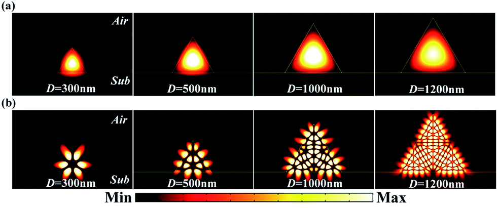 | ||
| Fig. 5 Simulation of near field E(x,y) patterns confined in GaN MWs with trilateral cross section, (a) the fundamental nonradiative modes; (b) the radiative modes. The diameter of GaN MWs changed from 300 nm to 1200 nm, parameters being used during numerical simulation nGaN = 2.89, nSub = 1.5, nAir = 1, with corresponding calculated wavelength λ = 375 nm. The center of the MW defines the origin (x = y = 0). | ||
Due to the inevitable waveguide loss of GaN MW, part of the excited photons of GaN MW would propagate along the axis of MW under optical pumping. There, the simulation model's result about waveguide mode transmission of a bare GaN MW placed on a substrate are shown in Fig. 6. This kind of model can be used to indicate the oscillation transmission process of the photons, which escaped from the F–P microcavity by means of 3D finite-difference time-domain (FDTD) methods. Fig. 6a–c shows the simulation of near field E(x,y) patterns on waveguide mode transmission of GaN MWs with TEM mode, TE mode, TM mode, respectively. As is well known, the oscillation pattern of the F–P cavity is relatively single, energy spread along the axis of the MW with a manner of oscillating back and forth inside the cavity. From this figure (three different waveguide modes), it can be seen that the photos of the cavity modes could be trapped inside the cavity body, and the corresponding standing wave pattern of the oscillation was formed between the two end faces of the microcavity. Perfect standing wave field distribution was observed and the wave beam could propagate back and forth between the two end faces of the microcavity to form the F–P resonance mechanism. It should be noted that a handful of the light escaped from the cavity and transfers to free space, indicating some optical loss at the GaN/air and GaN/substrate interface. The aforementioned discussion shows that the GaN MW can be used to realize F–P lasing quality due to the optical loss of the bare microcavity and the result is coincident with the experimental observation.
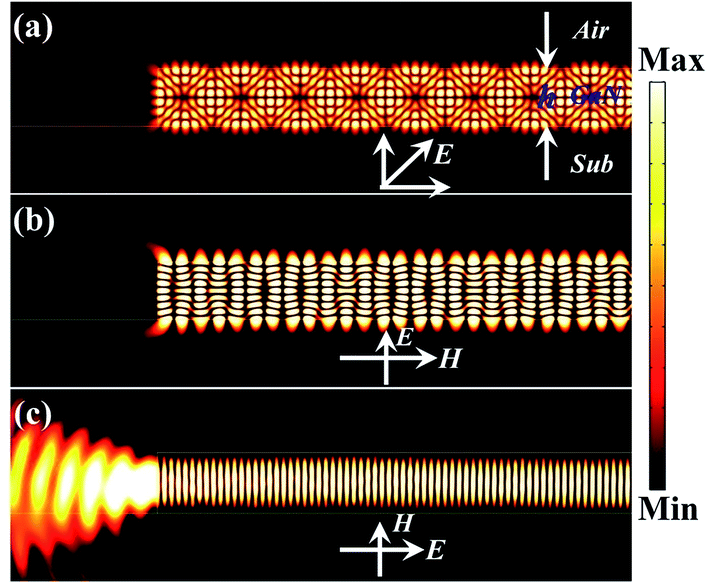 | ||
| Fig. 6 Simulation of near field E(x,y) patterns on waveguide mode transmission of the GaN MWs, with the size defined as h = 1.0 μm, length L = 15.0 μm. The parameters used during numerical simulation: nGaN = 2.89, nSub = 1.5, nAir = 1, with corresponding calculated wavelength λ = 375 nm. (a)TEM mode, no electric or magnetic field component in the propagation direction; (b)TE mode, with magnetic field component in the propagation direction but no electric field component; (c)TM mode, with electric field component in the propagation direction but no magnetic field component. | ||
Conclusions
In conclusion, a single nonpolar α-axial GaN MW was fabricated by MOCVD. The structure and optical properties of the GaN MWs were detail discussed. The D0X emission dominates in the low temperature range, and the FX emission dominates at high temperature in GaN MWs. Then stimulated emission was observed in the single GaN MW. The strongest laser mode occurs at 375 nm. The threshold is about 120 kW cm−2, the laser mode spacing is 0.8 nm. The original of the lasing of GaN MW is Fabry–Perot oscillations of two MW end facets. These results also agree with the simulation of GaN MW by FDTD. Thus, the GaN MW has a potential application for micro UV laser.Acknowledgements
This work is supported by National Natural Science Foundation of China Grant (No. 61205037, 61574063), Science and Technology Program of Guangdong Province, China (Grant No. 2016A040403106, 2014B040404067), Guangzhou Science and Technology Project (Grant No. 2016201604030047). The contact author would like to thank for the research fellowship offered by The University of Hong Kong and S. P. Wang for revised English.Notes and references
- S. Guha and N. A. Bojarczuk, Appl. Phys. Lett., 1998, 72, 415 CrossRef CAS.
- E. Monroy, E. Muoz, F. J. Snchez, F. Calle, E. Calleja, B. Beaumont, P. Gibart, J. A. Muoz and F. Cuss, Semicond. Sci. Technol., 1998, 13, 1042–1046 CrossRef CAS.
- S. Nakamura, G. Fasol and S. J. Pearton, Meas. Sci. Technol., 2001, 12, 777–786 CrossRef.
- W. C. Liao, S. W. Liao, K. J. Chen, Y. H. Hsiao, S. W. Chang, H. C. Kuo and M. H. Shih, Sci. Rep., 2016, 6, 26578 CrossRef CAS PubMed.
- H. T. Ng, J. Han, T. Yamada, P. Nguyen, Y. P. Chen and M. Meyyappan, Nano Lett., 2004, 4, 1247–1252 CrossRef CAS.
- Y. Yang, Q. Ji, H. Zong, T. Yan, J. Li, T. Wei and X. Hu, Opt. Commun., 2016, 374, 80–83 CrossRef CAS.
- P. Waltereit, H. Sato, C. Poblenz and D. S. Green, Appl. Phys. Lett., 2004, 84, 2748–2750 CrossRef CAS.
- C. T. Huang, J. Song, W. F. Lee, Y. Ding, Z. Gao, Y. Hao, L. J. Chen and Z. L. Wang, J. Am. Chem. Soc., 2010, 132, 4766–4771 CrossRef CAS PubMed.
- L. Lin, C. H. Lai, Y. Hu, Y. Zhang, X. Wang, C. Xu, R. L. Snyder, L. J. Chen and Z. L. Wang, Nanotechnology, 2011, 22, 475401–475405 CrossRef PubMed.
- S. Hao, G. Zhou, J. Wu, W. Duan and B. L. Gu, Phys. Rev. B: Condens. Matter Mater. Phys., 2004, 69, 113403 CrossRef.
- L. T. Fu, Z. G. Chen, D. W. Wang, L. Cheng, H. Y. Xu, J. Z. Liu, H. T. Cong, G. Q. Lu and J. Zou, J. Phys. Chem. C, 2010, 114, 9627–9633 CAS.
- P. C. Chang, Appl. Phys. Lett., 2007, 91, 051112 CrossRef.
- S. Li and A. Waag, J. Appl. Phys., 2012, 111, 071101 CrossRef.
- S. Pearton, GaN and ZnO-based Materials and Devices, Springer Berlin Heidelberg, 2012 Search PubMed.
- M. W. Lee, H. Z. Twu, C. C. Chen and C. H. Chen, Appl. Phys. Lett., 2001, 79, 3693–3695 CrossRef CAS.
- M. W. Lee, H. C. Hseuh, H. M. Lin and C. C. Chen, Phys. Rev. B, 2003, 67, 161309 CrossRef.
- C. C. Chen, C. C. Yeh, C. H. Chen, M. Y. Yu, H. L. Liu, J. J. Wu, K. H. Chen, L. C. Chen, J. Y. Peng and Y. F. Chen, J. Am. Chem. Soc., 2001, 123, 2791–2798 CrossRef CAS PubMed.
- W. Han, S. Fan, Q. Li and Y. Hu, Science, 1997, 277, 1287–1289 CrossRef CAS.
- F. Qian, S. Gradecak, Y. Li, C. Y. Wen and C. M. Lieber, Nano Lett., 2005, 5, 2287–2291 CrossRef CAS PubMed.
- S. Dhara, A. Datta, C. T. Wu, Z. H. Lan, K. H. Chen, Y. L. Wang, Y. F. Chen, C. W. Hsu, L. C. Chen and H. M. Lin, Appl. Phys. Lett., 2004, 84, 3486–3488 CrossRef CAS.
- T. Livneh, J. Zhang, G. Cheng and M. Moskovits, Phys. Rev. B: Condens. Matter Mater. Phys., 2006, 74, 2149 CrossRef.
- Y. D. Wang, S. J. Chua, S. Tripathy, M. S. Sander, P. Chen and C. G. Fonstad, Appl. Phys. Lett., 2005, 86, 071917 CrossRef.
- X. B. Chen, J. L. Morrison, J. Huso, L. Bergman and A. P. Purdy, J. Appl. Phys., 2004, 97, 024302 CrossRef.
- J. C. Johnson, H. J. Choi, K. P. Knutsen, R. D. Schaller, P. Yang and R. J. Saykally, Nat. Mater., 2002, 1, 106–110 CrossRef CAS PubMed.
- F. Qian, Y. Li, S. Gradečak, H. G. Park, Y. Dong, Y. Ding, Z. L. Wang and C. M. Lieber, Nat. Mater., 2008, 7, 701–706 CrossRef CAS PubMed.
- P. Lefebvre, J. Allègre, B. Gil, H. Mathieu, N. Grandjean, M. Leroux, J. Massies and P. Bigenwald, Phys. Rev. B: Condens. Matter Mater. Phys., 1999, 59, 15363 CrossRef CAS.
- P. Lefebvre, A. Morel, M. Gallart, T. Taliercio, J. Allègre, B. Gil, H. Mathieu, B. Damilano, N. Grandjean and J. Massies, Appl. Phys. Lett., 2001, 78, 1252–1254 CrossRef CAS.
- X. Wang, Y. Zhang, X. Chen, M. He, C. Liu, Y. Yin, X. Zou and S. Li, Nanoscale, 2014, 6, 12009–12017 RSC.
- X. Wang, J. Tong, X. Chen, B. Zhao, Z. Ren, D. Li, X. Zhuo, J. Zhang, H. Yi, C. Liu, F. Fang and S. Li, Chem. Commun., 2014, 50, 682–684 RSC.
- K.-W. Liu, S.-J. Chang, S.-J. Young, T.-H. Hsueh, H. Hung, Y.-C. Mai, S.-M. Wang and Y.-Z. Chen, J. Electrochem. Soc., 2011, 158, H983 CrossRef CAS.
- S. J. Xu, W. Liu and M. F. Li, Appl. Phys. Lett., 2000, 77, 3376–3378 CrossRef CAS.
- M. Leroux, N. Grandjean, B. Beaumont, G. Nataf, F. Semond, J. Massies and P. Gibart, J. Appl. Phys., 1999, 86, 3721–3728 CrossRef CAS.
- Y. P. Varshni, Physica, 1967, 34, 149–154 CrossRef CAS.
- R. Passler, E. Griebl, H. Riepl and G. Lautner, J. Appl. Phys., 1999, 86, 4403–4411 CrossRef CAS.
- H. Herr, V. Alex and J. Weber, MRS Online Proc. Libr., 2011, 482 Search PubMed.
- Y. Cui and C. M. Lieber, Science, 2001, 291, 851–853 CrossRef CAS PubMed.
- S. Adachi, Mater. Org., 1999, 88, 953–954 Search PubMed.
- M. Nami and D. F. Feezell, Opt. Express, 2014, 22, 29445–29455 CrossRef PubMed.
- A. Taflove and S. C. Hagness, Computational electrodynamics, Artech house, 2005 Search PubMed.
| This journal is © The Royal Society of Chemistry 2017 |