
 Open Access Article
 This Open Access Article is licensed under a Creative Commons Attribution-Non Commercial 3.0 Unported Licence
Effect of an external electric field on the electronic properties of SnS2/PbI2 van der Waals heterostructures
Yaqiang Ma a,
Xu Zhao*a,
Mengmeng Niua,
Xianqi Dai*ab,
Wei Lia,
Yi Lia,
Mingyu Zhaoa,
Tianxing Wanga and
Yanan Tangb
a,
Xu Zhao*a,
Mengmeng Niua,
Xianqi Dai*ab,
Wei Lia,
Yi Lia,
Mingyu Zhaoa,
Tianxing Wanga and
Yanan Tangb
aCollege of Physics and Materials Science, Henan Normal University, Xinxiang, Henan 453007, China. E-mail: zhaoxu@htu.cn; xqdai@htu.cn
bSchool of Physics and Electronic Engineering, Zhengzhou Normal University, Zhengzhou, Henan 450044, China
First published on 12th May 2017
Abstract
The future development of optoelectronic devices will require an advanced control technology in electronic properties, for example by an external electric field (Efield). Here we demonstrate an approach that the heterostructure based on van der Waals (vdW) heterobilayer built by monolayer SnS2 and PbI2 has a well-controlled electronic properties with Efield. A type-II staggered-gap band alignment is achieved from the SnS2/PbI2 vdW heterostructure with which SnS2 dominated the lowest energy holes as well as the lowest energy electrons are separated in PbI2. The charge redistribution with an Efield is mainly on the surface of SnS2 layer and PbI2 and the numbers of polarized electrons on the monolayers display a linear evaluation with external Efield. The band structure under different Efield experiences not only a transition from semiconductor to metal but also conversions between type-I straddling-band alignment and type-II staggered-gap, which results in different spatial distribution of the lowest energy electrons and holes. Moreover, when the Efield is between −0.06 V Å−1 and −0.34 V Å−1, the material manifests a varied direct bandgap which is more favor to optoelectronics and solar cell. Consequently, this vdW heterobilayer with well-controlled manner shows expectation for huge potential in optics and electronics.
1. Introduction
Ever since the successful manufacture of isolated graphene was reported,1 two dimensional (2D) materials have become the subject of extensive research because of their superior optical and electronic properties. Hence, a broad family of 2D materials like graphene, such as BN,2 transition metal dichalcogenides3–5 and topological insulators6–8 etc., has been widely explored to solve that pristine graphene has a zero bandgap. Among them, recently, the SnS2 2D films9,10 have been poured unordinary attentions due to environmentally friendly and earth-abundant. For instance, it was reported that SnS2 can be used as advance materials for photocatalytic,11 field effect transistors12 and anode in lithium batteries.13 Meanwhile, previous studies on the lamellar semiconductor material of PbI2 have reported that the freestanding single crystals PbI2 could be prepared by a facile way.14 Furthermore, PbI2 has been demonstrated to be an attractive candidate of thin film transistors and can play the role of a precursor for the organ PbI2 perovskites employed in highly efficient hybrid solar cells.15–17 Accordingly, SnS2 and PbI2 have promising potential applications in optics and electronics.For the sake of exploring materials in electronics, optoelectronics and photovoltaics devices, 2D materials can be used as building blocks restacked layer-by-layer in precisely chosen sequences yielding composites with unusual properties.18,19 A brand new discipline is provided to tailor electronic and optical properties of 2D materials into new physics and device applications owing to their unique crystal properties. For instance, an enterprising and insightful approach has been recently exhibited that an atomically thin p–n diode can be manufactured by a vertically stacked heterobilayer between n-type MoS2 and p-type WSe2 slices,20,21 which will not lead to doping problems.22 Moreover, properties of vdW heterostructure would be more excellent than building blocks such as the SnS2/MoS2 vdW heterostructure exhibit an obvious photovoltaic effect and possess high mobility (27.6 cm2 V−1 s−1), high on/off ratio (>106) and high photoresponsivity (1.36 A W−1), which is more outstanding than SnS2 and MoS2.23 Thus, the vdW heterostructure with novel electronic and optoelectronic properties will reveal favorable properties and novel phenomena.
It is crucial to modify electronic properties of 2D materials for application in semiconductor devices and the two more effective ways are straining24,25 and Efield.26,27 In this article, we employed an external Efield to tunable the band structures because of reversibility and easy achievement. A quintessential example should be cited that the bandgap of bilayer graphene can be efficiently switched on via applications of electric field because the inversion symmetry of the structure was destroyed.28,29 The fundamental bandgap of MoS2, MoSe2, MoTe2 and WS2 bilayer structures could be continuously modified with applied electric fields, eventually rendering them metallic.30–32 Accordingly, utilization of Efield would lead to the realization of electronic properties engineering of the materials.
The bandgap of homobilayer SnS2 could be continuously decreased with the electric field as well as different stacks33 and a robust indirect band structure accompanied with the strength of increasing Efield. However, it is well known that the electron–hole recombination lifetime of the indirect bandgap semiconductor is longer than direct bandgap leading to lower the luminous efficiency, which is inappropriate for optoelectronic devices. Despite lots of researchers force on the modulation electronic properties of SnS2 such as doping and strain,10,12 there is no literature on SnS2 with a direct bandgap.
In this work, we investigated the vdW heterostructure restacked by SnS2 monolayer and PbI2 monolayer to engineer an alternative type of advance optoelectronic material to realize any practical application of 2D vdW p–n junctions. The electronic properties have been systematically studied with external Efield by theoretical simulation and a well-behaved was found. The features make SnS2/PbI2 vdW heterobilayer a promising material for the advantage optoelectronic devices.
2. Theoretical methods
Our calculations were performed based on the density functional theory (DFT) in conjunction with the projector-augmented wave (PAW) potentials34 as implemented in the Vienna Ab initio Simulation Package (VASP).35,36 The exchange–correlation potentials was described through the Perdew–Burke–Ernzerhof (PBE) functional within the generalized gradient approximation (GGA) formalism.37 The valence electron configurations for Sn, S, Pb and I were 4d105s25p2, 3s23p4, 5d106s26p2 and 5s25p5, respectively. The heterobilayer was built by cells of SnS2 and 2 × 2 cells of PbI2. That a plane wave basis set with a cutoff energy of 480 eV and a 5 × 5 × 1 k-points grids determined by a fine grid of gamma-centered Monkhorst–Pack method38 in the Brillouin zone was found to give good converged results. The atomic structures were relaxed using conjugate gradient algorithm as implemented in the VASP code until the forces on all unconstrained atoms were smaller than 0.01 eV Å−1. Moreover, a more precise method for the on-site Coulomb repulsion of Sn 4d and Pb 5d was considered in all calculations for the sake of more accurate bandgap. A PBE+U approach39 was employed to treat exchange–correlation energy and the choice of U = 9 eV for Sn as well as 8.5 eV for Pb can reproduce the experimental bandgap of SnS2 and PbI2, respectively. Additionally, spin-orbital-coupling40 was expected to be significant influence on the heavy atoms of lead (Pb), therefore it was considered in all calculation. A vacuum layer of 20 Å along z direction was constructed to eliminate the interaction with spurious replica images. The zero damping DFT-D3 method of Grimme41 was used to account for long range vdW interaction between monolayer SnS2 and PbI2. All of structural figures and charge density drawings were produced by VESTA package.42
3. Results and discussion
The schematic illustration of monolayer SnS2 and PbI2 is displayed in Fig. 1. Primitive cells are plotted by a black line and a brief look for the vector of lattices is marked. After the total energy optimization, the lattice constants of monolayer SnS2 and PbI2 are respectively collected as 3.61 Å and 4.67 Å as exhibited in Table 1, that the agreements with previous studies are preeminent.8,22,32 The properties of monolayer SnS2 and PbI2 are intensely sensitive to in-plane strains43,44 so that the impact of strain on electronic structure should be reduced. To minimize the lattice mismatch between the stacking blocks, the supercell of this heterostructure is built by of SnS2 cells and 2 × 2 of PbI2 cells, which the maximum mismatch for both SnS2 and PbI2 lattices is less than 2.3%.
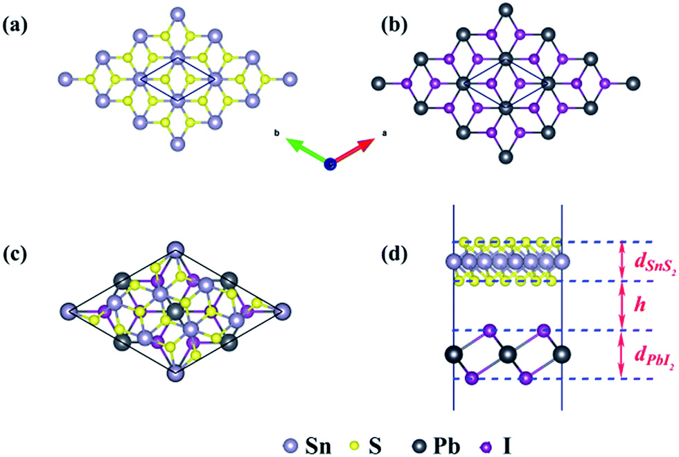 | ||
| Fig. 1 Schematic of the monolayers and the SnS2/PbI2 vdW heterobilayer. Top view of (a) SnS2 and (b) PbI2 monolayer. The top (c) and side view (d) of the heterobilayer. Silvery, yellow, dark grey and purple spheres represent Sn, S, Pb and I atoms, respectively. | ||
| a (Å) | d (Å) | h (Å) | ||
|---|---|---|---|---|
| SnS2 monolayer | 3.61 | 2.98 | ||
| PbI2 monolayer | 4.67 | 3.72 | ||
| The heterostructure | SnS2 monolayer | 9.45 | 3.03 | 3.49 |
| PbI2 monolayer | 3.68 | |||
The top and across views of the SnS2/PbI2 vdW heterostructure is presented in Fig. 1(c) and (d). The thicknesses of monolayers and the distance between SnS2 and PbI2 single-layer are respectively marked with d and h as displayed in Fig. 1(d). The optimized structural parameters and the binding energies are given in Table 1. After fully relaxed, the interlayer distance (h = 3.49 Å) is far greater than the sum of the covalent radii of I and S atom, indicating that the two building blocks are beyond the bonding range. To evaluate the stability, the binding energy (ΔEb) of SnS2/PbI2 vdW heterobilayer was calculated and defined by,
| ΔEb = (ESnS2/PbI2 − ESnS2 − EPbI2)/n, | (1) |
The binding energy of SnS2 and PbI2 vdW heterobilayer is −0.124 eV per SnS2 unit, which is indicative of a rather weak but stable interaction between the layers. This could be just more evidence for that the interaction between SnS2 monolayer and PbI2 monolayer is mainly forced through van der Waals interactions because ΔEb has the same order of magnitude as the other vdW substances, for example, graphite (ΔEb = −0.10 eV per C atom),45 bilayer SnS2 (ΔEb = −0.05 eV per SnS2 unit),33 the MoS2/PbI2 heterostructure (ΔEb = −0.234 eV per MoS2 unit)46 and black phosphorus/MoS2 heterobilayer (ΔEb = −0.108 eV per MoS2 unit).47
We calculate the band structures of monolayer SnS2 (Fig. 2(a)) and PbI2 (Fig. 2(b)) as well as the SnS2 and PbI2 vdW heterostructure (Fig. 2(c)) to obtain the electronic properties based on PBE+U approach. For SnS2 monolayer, the fundamental band structure is an indirect bandgap of about 2.22 eV that the valance band maximum (VBM) is extremely close to Γ point and the conduction band minimum (CBM) lies at M which is close to the reported values.12,48 Additionally, the smallest gap of PbI2 monolayer appears between the CBM at Γ and the VBM which medially lies between K and Γ that the agreements with previous studies are preeminent.43
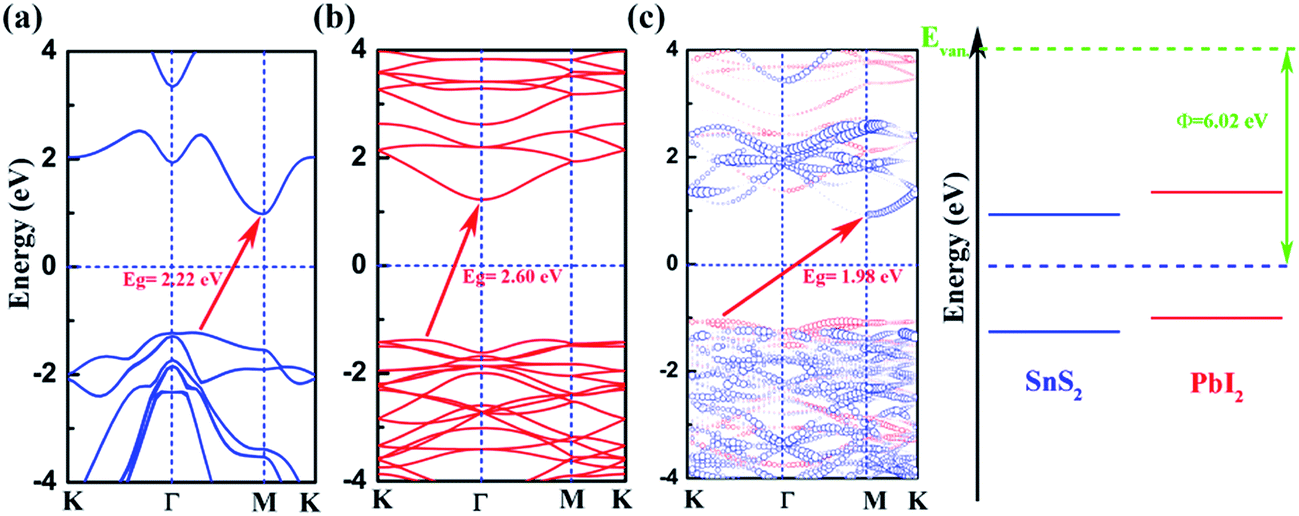 | ||
| Fig. 2 Electronic band structures of (a) PbI2, (b) SnS2. (c) The projected band structure as well as schematic of band alignment of SnS2/PbI2 vdW heterostructure (blue and red lines respectively represent for SnS2 and PbI2 layer). The Fermi level is set to zero and marked by horizontal blue dotted line. The vacuum level is taken as a reference marked by green horizontal dash. | ||
In Fig. 2(c), we present the projected band structure of the SnS2 and PbI2 in the vdW heterobilayer that the blue lines represent of SnS2 monolayer and the red lines are for PbI2, respectively. As can be seen in Fig. 2(c), the SnS2 monolayer and PbI2 monolayer compose a type-II staggered-gap band alignment that the CBM is contributed by SnS2 whereas the VBM by PbI2 with a bandgap of about 1.98 eV. In consequence, the Fermi level shifts to the CBM of SnS2 and VBM of PbI2 after they compose the heterobilayer. It can be looking forward that the photoelectric property will be improved distinctively because the lowest energy electron–hole pairs can separate in real space. Compared with the band structure, band alignment of heterostructure are even more important in material and device design. Meanwhile, the work function (Φ = EVan − EF, where the EVan is the vacuum level and the EF is the Fermi level, respectively) and band alignment is shown in Fig. 2(d). It is indicated that a type-II band alignment of vdW heterostructure is formed at the SnS2/PbI2 interface which will spontaneously separate the free electrons and holes, enabling the high efficiency optoelectronics and solar energy conversion.
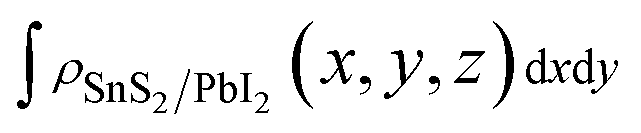
To shed more lights on the nature of the charge transfer between the SnS2 and PbI2 layer, the averaged difference electron density of the heterostructure along the z direction was calculated by the formula
 | (2) |
 ,
,  and
and  are the charge density at the (x, y, z) point in the SnS2/PbI2 bilayer, SnS2 and PbI2 monolayer, respectively. Accordingly, a positive value means electron accumulation and negative for depletion. The result is exhibited in Fig. 3(a), that the vertical blue short dash line means the intermediate position for the interface of the building blocks as well as the positions of Sn, S, Pb and I atomic layers are marked as purple, dark grey, yellow and silvery and short dot lines, respectively. As a result of the interlayer coupling effect, there is an obvious charge accumulation region as the SnS2/PbI2 heterointerface. Moreover, there is a small amount of electrons (about 0.453 × 10⁻³|e|) transferring from PbI2 to SnS2 layer, further indicating a weak interlayer coupling between SnS2 layer and PbI2 layer. Furthermore, a built-in electrical field formed intrinsic spontaneous of electric polarization is expected and directed from PbI2 to SnS2.
 | ||
| Fig. 3 (a) The averaged difference electron density of SnS2/PbI2 heterostructure along z direction. (b) and (c) The integrated charge density difference of the heterobilayer under different external Efield. (d) The transferred electrons as a function of Efield. The positive values of electrons in (d) indicate a transferred direction from SnS2 to PbI2 layer. | ||
It is crucial to modify electronic properties of 2D materials for application in semiconductor devices so that an external Efield perpendicular to the heterobilayer is employed. The positive direction of Efield is set from PbI2 layer to SnS2 layer. To evaluate the influences of Efield modulating on the electronic properties of the heterostructure, the integrated charge density difference with Efield along z direction was employed and determined as,
 | (3) |
 and
and  are the charge density at (x, y, z) point of SnS2/PbI2 heterostructure with and without Efield. The results are displayed in Fig. 3(b) and (c). It is obvious that the charge redistribution is mainly on the surface of SnS2 and PbI2 layers. The positive charges (holes) tend to transfer from SnS2 layer to PbI2 layer and negative charges (electrons) transfer from PbI2 layer to SnS2 layer in the case of a negative Efield as well as positive Efield lead to the opposite direction of charge and hole transfers. Additionally, the amount of transferring electrons depends on the strength of the applied Efield.
To shed more lights on the charge redistribution with Efield, the numbers of polarized electrons on the building blocks were obtained through integrating the charge density from the vacuum layer to the intermediate position of the interface of the monolayers as exhibited in Fig. 3(d). The positive value means the electron transfers from SnS2 layer to PbI2 layer. The numbers of polarized electrons on the building blocks display a linear evaluation with external Efield and a transitional on the direction depends on the direction of Efield is found, which is identical with above analyses. The accumulation of electrons (holes) will lead to the Fermi level down (up)-shifted of SnS2 and PbI2 monolayer which thereby bring about modulation of the band structure. More charge transfer between SnS2 and PbI2 layer heralds a stronger interlayer interaction, indicating the shifts of band edges.
This could be graphically explained in Fig. 4(a), which manifests the evolution of the bandgap of SnS2/PbI2 heterostructure as a function of applied Efield. The bandgap is continuously tuned under the Efield, eventually achieving a mutation from semiconductor to metal at critical Efield. The bandgap varies linearly with Efield indicating a giant Stark effect.49 It is almost lineally reduced with the strength of Efield reducing to zero bandgap at the Efield of about 0.28 V Å−1 when a forward voltage is applied. For a negative Efield, the bandgap firstly increases reaching up to 2.19 eV which appears at an Efield of about −0.03 V Å−1. The encouragement of bandgap is due to the presence of intrinsic spontaneous of electric polarization which is opposite to the Efield and has a superimposing effect on it. Further increases in strength of negative Efield (|Efield| > 0.06 V Å−1) lead to linearly decreases in bandgap and the heterobilayer turns metallic at about −0.34 V Å−1.
 | ||
| Fig. 4 (a) Bandgap variation with applied Efield of the SnS2/PbI2 vdW heterostructure. (b) Evolution of the band edges in SnS2/PbI2 heterostructure as a function of the Efield. CBMSnS2(PbI2) and VBMSnS2(PbI2) are the CBM and VBM of SnS2(PbI2) in the vdW heterobilayer. | ||
To gain further insight, band edges dominated by SnS2 and PbI2 under various Efield are calculated and displayed in Fig. 4(b). The CBM and VBM of SnS2(PbI2) of the vdW heterobilayer are denoted by CBMSnS2(PbI2) and VBMSnS2(PbI2), respectively. Both the CBM and VBM of SnS2 decrease linearly with Efield while the CBM and VBM of PbI2 manifest a linear increase. The Efield exerts litter influence on the respective bandgaps of SnS2 and PbI2. The bandgap of SnS2/PbI2 heterostructure gives the same variation trend with Fig. 4(a). Additionally, the band alignment conversion from type-II to type-I heterostructure separated by the Efield about −0.03 V Å−1 and then from type-I to type-II by about −0.06 V Å−1, resulting in different spatial distribution of the lowest energy electrons and holes.
Energy dispersion with and without Efield is displayed in Fig. 5(a)–(d), respectively. With an Efield of −0.15 V Å−1, the heterobilayer manifests a direct bandgap that both the CBM and VBM are located at Γ point. The direct bandgap semiconductor has a less electron–hole recombination lifetime with a high luminous efficiency which is overwhelmingly suitable for optoelectronic devices. The location of CBM changes from Γ to M point in the Brillouin zone but the VBM is still at Γ point leading to an indirect bandgap in the case of Efield = −0.05 V Å−1 as shown in Fig. 5(b). When an Efield of 0.15 V Å−1 is added to the vdW heterostructure, the band structure manifests an indirect bandgap that the CBM located at M point and VBM between K to Γ point (Fig. 5(d)).
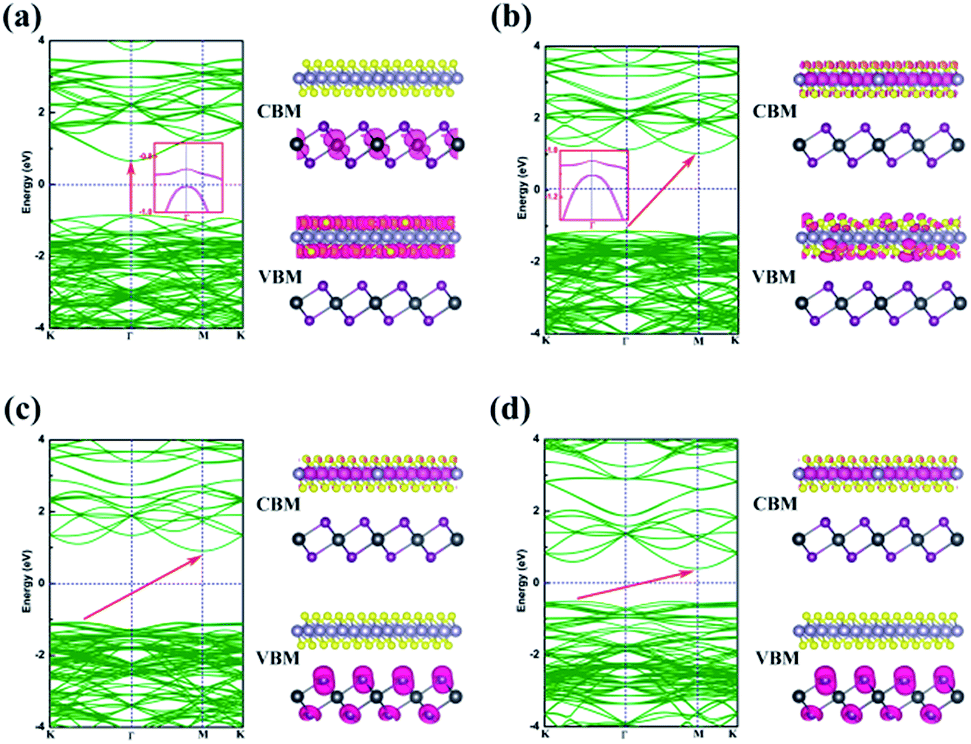 | ||
| Fig. 5 Band structures and partial charge densities plot for the CBM and VBM of the SnS2/PbI2 vdW heterostructure with and without Efield. (a) Efield = −0.15 V Å−1, (b) Efield = −0.05 V Å−1, (c) Efield = 0 V Å−1, and (d) Efield = 0.15 V Å−1. All isosurfaces of this text are set to 0.004 e Å−3. | ||
The partial charge densities of the heterostructure from CBM and VBM with different Efield are calculated and summarized in Fig. 5. When the SnS2/PbI2 vdW heterobilayer subjected to a negative Efield of −0.15 V Å−1, it is clearly shown that the partial charge density from CBM is dominated by Pb atoms and the VBM comes mainly from the SnS2 layer, as shown in Fig. 5(a). That is to say, the staggered-gap band alignment be suggestive of a type-II heterojunction. Both the CBM and VBM of the heterobilayer, when the heterobilayer suffered by an Efield of −0.05 V Å−1, are all straddled by SnS2 layer (Fig. 5(b)) indicating a type-I heterojunction. When the heterobilayer suffered by the Efield of 0 V Å−1 or 0.15 V Å−1, the partial charge density from CBM is dominated by Sn atoms and the VBM by I atomical layer displayed in Fig. 5(c) and (d), respectively. Thus, a type-II staggered-gap band alignment is obtained with an alternation of CBM and VBM between the monolayer SnS2 and PbI2. Briefly, the band structures can be effectively modulated by an external electric field.
Similar evidence also comes from the band alignment of SnS2/PbI2 heterostructure under various Efield, as seen in Fig. 6. The Ef-SnS2(PbI2) indicate the quasi-Fermi level of SnS2(PbI2) in the vdW heterobilayer. VD denote the conduction band offset in the SnS2/PbI2 heterostructure without an Efield as well as V = Efield × d is the external electric potential, which leads to the divergence of the quasi-Fermi levels. The interlayer distance is marked with d, which is a constant in this case. When the SnS2/PbI2 vdW heterostructure subjected to a negative Efield, the bandgap varies with Efield in the following function:
| Eg = Eg(SnS2) − e(VD − V) = Eg(SnS2) − eVD + eEfield × d. | (4) |
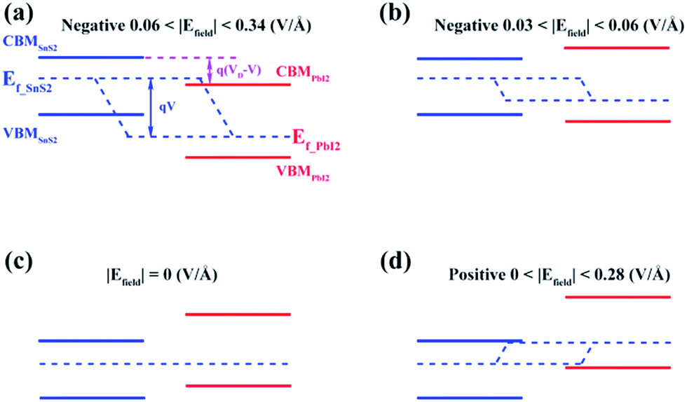 | ||
| Fig. 6 Band alignments of the SnS2/PbI2 vdW heterobilayer under different Efield. | ||
The maximum bandgap is obtained when the Efield reaches to −0.03V Å−1. Even the electric field increasing to −0.06V Å−1, both the CBM and VBM of the heterobilayer are all straddled by SnS2 layer. So, bandgap can be obtained as,
| Eg = Eg(SnS2) ≈ 2.19 eV. |
Under circumstances of Efield greater than 0.06 V Å−1 along the negative direction, the bandgap varies as the function:
| Eg = Eg(SnS2) − e(Efield − 0.06)d. |
The linear evaluations of bandgap with the strength of Efield are obtained as the Eg(SnS2) and e is constant. Meanwhile, the varied relationship between bandgap and Efield shares the same evidence of the giant Stark effect.
4. Conclusions
In summary, a vdW heterostructure of SnS2 and PbI2 has been theoretically simulated and the heterobilayer has a well-behaved electronic property under an external Efield. A type-II staggered-gap band alignment is constituted which the spatial separation of the lowest energy electron–hole pairs can be actualized. When suffered under an external Efield, the charge redistribution is mainly on the surface of SnS2 and PbI2 layers and the numbers of polarized electrons on the building blocks display a linear evaluation with external Efield. Meanwhile, the transitional direction depends on the direction of Efield. The external Efield not only influences the band structure which changes from semiconductor to metal but also forces on band alignment which experiences a conversion between type-I straddling-band alignment type-II broken-gap, leading to a different spatial distribution of the lowest energy electrons and holes. A direct bandgap of the heterobilayer is found among −0.06 V Å−1 and −0.34 V Å−1. This work could bring forward a new perspective on advantage optoelectronics devices with a well-Efield-controlled manner by using SnS2/PbI2 vdW heterostructure.Acknowledgements
This work was financially supported by the National Natural Science Foundation of China (Grant no. 61674053, 11504092 and 11504334), the Natural Science Foundation of Henan Province (Grant No. 162300410325) and by the High Performance Computing Center of Henan Normal University.References
- K. S. Novoselov, A. K. Geim, S. V. Morozov, D. Jiang, Y. Zhang, S. V. Dubonos and A. A. Firsov, Science, 2007, 306, 666–669 CrossRef PubMed.
- L. Wirtz, A. Marini and A. Rubio, Phys. Rev. Lett., 2005, 96, 126104 CrossRef PubMed.
- Q. Wang, K. Kalantar-Zadeh, A. Kis, J. Coleman and M. S. Strano, Nat. Nanotechnol., 2012, 7, 699–712 CrossRef CAS PubMed.
- W. Li, T. Wang, X. Dai, X. Wang, C. Zhai, Y. Ma and S. Chang, Solid State Commun., 2016, 250, 9–13 CrossRef.
- H. Liu, H. Zheng, F. Yang, L. Jiao, J. Chen, W. Ho, C. Gao, J. Jia and M. Xie, ACS Nano, 2015, 9, 6619–6625 CrossRef CAS PubMed.
- S. Zhang, B. Bernevig and T. Hughes, Science, 2007, 314, 1757–1761 Search PubMed.
- X. Zhao, X. Dai, B. Zhao, N. Wang and Y. Ji, J. Phys.: Condens. Matter, 2013, 25, 265005 CrossRef PubMed.
- B. Li, X. Guo, W. Ho and M. Xie, Appl. Phys. Lett., 2015, 107, 081604 CrossRef.
- R. RMitchell, Y. Fujiki and Y. Ishizawa, Nature, 1974, 247, 537–538 CrossRef.
- C. Xia, X. Zhao, Y. Peng, H. Zhang, S. Wei and Y. Jia, Superlattices Microstruct., 2015, 85, 664–671 CrossRef CAS.
- Y. Sun, H. Cheng, S. Gao, Z. Sun, Q. Liu, Q. Liu, F. Lei, T. Yao, J. He, S. Wei and Y. Xie, Angew. Chem., 2012, 51, 8727–8731 CrossRef CAS PubMed.
- C. Xia, Y. Peng, H. Zhang, T. Wang, S. Wei and Y. Jia, Phys. Chem. Chem. Phys., 2014, 16, 19674–19680 RSC.
- M. He, L. Yuan and Y. Huang, RSC Adv., 2013, 3, 3374–3383 RSC.
- X. Zhu, Y. Wang, H. Sun, D. Yang, X. Gao and H. Tian, Mater. Lett., 2016, 180, 59–62 CrossRef CAS.
- H. Wang, X. Hu and H. Chen, RSC Adv., 2015, 5, 30192–30196 RSC.
- A. Kojima, K. Teshima, Y. Shirai and T. Miyasaka, J. Am. Chem. Soc., 2009, 131, 6050 CrossRef CAS PubMed.
- A. Abate, M. Planells, D. J. Hollman, V. Barthi, S. Chand, H. J. Snaith and N. Robertson, Phys. Chem. Chem. Phys., 2014, 17, 2335 RSC.
- A. K. Geim and I. V. Grigorieva, Nature, 2013, 499, 419 CrossRef CAS PubMed.
- Q. Sun, Y. Dai, Y. Ma, N. Yin, W. Wei, L. Yu and B. Huang, 2D Mater., 2016, 3, 035017 CrossRef.
- R. Cheng, D. Li, H. Zhou, C. Wang, A. Yin, S. Jiang, Y. Liu, Y. Chen, Y. Huang and X. Duan, Nano Lett., 2014, 14, 5590–5597 CrossRef CAS PubMed.
- N. Huo, J. Yang, L. Huang, Z. Wei, S. Li, Z. Wei and J. Li, Small, 2015, 11, 5430–5438 CrossRef CAS PubMed.
- M. M. Furchi, A. A. Zechmeister, F. Hoeller and S. Wachter, IEEE J. Sel. Top. Quantum Electron., 2015, 14, 8 Search PubMed.
- B. Li, L. Huang, M. Zhong, Y. Li, Y. Wang, J. Li and Z. Wei, Adv. Electron. Mater., 2016, 2, 1600298 CrossRef.
- L. Huang, Y. Li, Z. Wei and J. Li, Sci. Rep., 2015, 5, 16448 CrossRef CAS PubMed.
- W. Xiong, C. Xia, X. Zhao, W. Wang and Y. Jia, Carbon, 2016, 109, 737–746 CrossRef CAS.
- W. Li, T. Wang, X. Dai, Y. Ma and Y. Tang, J. Alloys Compd., 2017, 705, 486–491 CrossRef CAS.
- C. Xai, B. Xue, T. Wang, Y. Peng and Y. Jia, Appl. Phys. Lett., 2015, 107, 193107 CrossRef.
- E. Mccann, Phys. Rev. B: Condens. Matter Mater. Phys., 2006, 74, 161403 CrossRef.
- M. K. Madito, N. Manyala, A. Bello, J. K. Dangbegnon, T. M. Masikhwa and D. Y. Momodu, RSC Adv., 2016, 6, 28370–28378 RSC.
- A. Ramasubramaniam, D. Naveh and E. Towe, Phys. Rev. B: Condens. Matter Mater. Phys., 2011, 84, 203239–203247 Search PubMed.
- Z. Huang, C. He, X. Qi, H. Yang, W. Liu, X. Wei, X. Peng and J. Zhong, J. Phys. D: Appl. Phys., 2014, 47, 75301–75306 CrossRef.
- L. Huang and J. Li, Appl. Phys. Lett., 2016, 108, 147 Search PubMed.
- P. Guo, T. Wang, C. Xia and Y. Jia, Appl. Phys. A, 2016, 122, 1–7 CrossRef CAS.
- G. Kresse and D. Joubert, Phys. Rev. B: Condens. Matter Mater. Phys., 1999, 59, 1758–1775 CrossRef CAS.
- G. Kresse and J. Furthmüller, Comput. Mater. Sci., 1996, 6, 15–50 CrossRef CAS.
- P. E. Blöchl, Phys. Rev. B: Condens. Matter Mater. Phys., 1994, 50, 17953–17979 CrossRef.
- J. P. Perdew, K. Burke and M. Ernzerhof, Phys. Rev. Lett., 1996, 77, 3865 CrossRef CAS PubMed.
- H. J. Monkhorst and J. D. Pack, Phys. Rev. B: Condens. Matter Mater. Phys., 1976, 13, 5188 CrossRef.
- S. Dudarev, G. Botton, S. Savrasov, C. Humphreys and A. Sutton, Phys. Rev. B: Condens. Matter Mater. Phys., 1998, 57, 1505–1509 CrossRef CAS.
- A. Bermudez, F. Jelezko, M. B. Plenio and A. Retzker, Phys. Rev. Lett., 2011, 107, 3745 Search PubMed.
- S. Grimme, J. Antony, S. Ehrlich and H. Krieg, J. Chem. Phys., 2010, 132, 154104–154119 CrossRef PubMed.
- K. Momma and F. Izumi, J. Mineral. Petrol. Sci., 2010, 39, 136–145 CAS.
- M. Zhou, W. Duan, Y. Chen and A. J. Du, Nanoscale, 2015, 7, 15168–15174 RSC.
- B. Ram, A. Manjanath and A. K. Singh, 2D Mater., 2016, 3, 015009 CrossRef.
- G. Graziano, J. Klimeš, F. Fernandez-Alonso and A. Michaelides, J. Phys.: Condens. Matter, 2012, 24, 424216 CrossRef PubMed.
- Y. Ma, X. Zhao, T. Wang, W. Li, X. Wang, S. Chang, Y. Li, M. Zhao and X. Dai, Phys. Chem. Chem. Phys., 2016, 18, 28466 RSC.
- L. Huang, N. Huo, Y. Li, H. Chen, J. Yang, Z. Wei and J. Li, J. Phys. Chem. Lett., 2015, 6, 2483 CrossRef CAS PubMed.
- L. A. Burton, T. J. Whittles, D. Hesp, W. M. Linhart, J. M. Skelton, B. Hou, R. F. Webster, G. O'Dowd, C. Reece, D. Cherns, D. J. Fermin, T. D. Veal, V. R. Dhanak and A. Walsh, J. Mater. Chem. A, 2016, 4, 1312 CAS.
- F. Zheng, Z. Liu, J. Wu, W. Duan and B. Gu, Phys. Rev. B: Condens. Matter Mater. Phys., 2008, 78, 085423 CrossRef.
| This journal is © The Royal Society of Chemistry 2017 |