
 Open Access Article
 This Open Access Article is licensed under a
 Creative Commons Attribution 3.0 Unported Licence
Oxide-induced grain growth in CZTS nanoparticle coatings†
Stephen Exarhosa,
Edgar Palmesb,
Rui Xua and
Lorenzo Mangolini *ab
*ab
aDepartment of Mechanical Engineering, Bourns College of Engineering, University of California, Riverside, Riverside, CA, USA
bDepartment of Materials Science & Engineering, Bourns College of Engineering, University of California, Riverside, Riverside, CA, USA. E-mail: lmangolini@engr.ucr.edu
First published on 12th May 2017
Abstract
An innovative and scalable synthesis approach to the formation of CZTS nanoparticles has been developed using aerosol spray pyrolysis. Surface-ligand-free CZTS nanoparticles with controllable size and composition are synthesized by thermally decomposing an aerosolized precursor mixture of copper, zinc, and tin thiocarbamates. After collection, the particles are dispersed in an organic solvent, coated on soda lime glass, mechanically compacted, and annealed in a low-pressure sulfur atmosphere to form CZTS thin films. The resulting thin film is highly porous and composed of small grains. We have found that growing a thin amorphous oxide layer on the surface of ligand-free Cu2ZnSnS4 (CZTS) nanoparticles substantially enhances uniform grain growth during heat treatment in a sulfur atmosphere. This is achieved by adding a simple annealing step in air after nanoparticle production and before coating. This process consistently results in CZTS films with higher tin content after annealing, suggesting that the presence of an oxide layer around the particles improves the retention of volatile tin sulfide phases, which is then beneficial in respect to grain growth kinetics.
Introduction
Cu2ZnSnS4 (CZTS) is a potential absorber layer material for thin film photovoltaic (PV) applications. The constituent elements of CZTS are inexpensive and earth-abundant, therefore advantageous compared to alternative materials like CdTe and Cu(In,Ga)Se2.1–4 The state of the art CZTS devices have achieved a power conversion efficiency of 12.6% (in this case with selenium alloyed in conjunction with sulfur to make CZTSSe).5 This is significantly lower than the ∼30% maximum theoretical efficiency for this material determined by the Shockley–Queisser limit.6A recent review by Liu et al. intended to identify key aspects to improving efficiency in kesterite-based PVs.7 The authors target the optimization of the device structure, specifically interfaces between the kesterite absorber layer and the back contact and between the absorber and the buffer layer. They also note the importance of using material composition as a means of promoting beneficial defects like CuZn or VCu, while suppressing detrimental defects like SnZn.7 In addition, the role of grain boundaries in the optoelectronic properties of CZTS thin films is still not clear. This problem is exacerbated by the fact that the correlation between synthesis and processing parameters and the morphology of the resulting films is still under intense investigation.
CZTS can be synthesized by a variety of methods, including co-evaporation, sputtering, electrodeposition, and solution-based processes. CZTS can also be made in nanoparticle form by various methods. Nanoparticle-based manufacturing schemes are generally considered to be more cost-effective and scalable than other (especially vacuum-based) film fabrication approaches. The most common CZTS nanoparticle synthesis method is hot-injection,1,8,9 though solvothermal10–12 and microwave-assisted synthesis13,14 have also been reported as successful. All of these methods require a sulfur or selenium annealing process to obtain a dense film with large grains. For this reason it is crucial to understand the parameters that control the sintering of CZTS nanoparticles during the sulfurization (or selenization) process.
Sodium doping has been shown to enhance grain growth, and subsequently device performance, in the CZTS system.15–19 By comparing the growth of CZTS crystal grains on substrates with and without sodium, enhanced grain growth was concluded to be an effect of sodium and other alkali diffusion from the substrate into the film material.20
Alternatively, organic ligands have also been proposed as being beneficial in promoting grain growth in CZTS/CZTSSe nanoparticle systems. Martin et al. compared the effect that two different nanoparticle-capping ligands, derived from oleylamine (OLA) and dodecylamine respectively in a hot-injection process, had on the crystallinity of the annealed CZTSSe film.21 The conclusion was that the longer ligands from the OLA yielded vastly superior crystallinity and uniformity after annealing. Huang et al. have produced a similar study in CZTS, comparing the crystallinity of films derived from OLA-synthesized CZTS nanoparticles and formamide-synthesized CZTS nanoparticles.22 However, with carbon introduced to the system, these same groups report highly crystalline thin films in the case of the higher-carbon content ligands, but with a detrimental carbon-rich fine-grain layer sandwiched between the substrate and the CZTS or CZTSSe film.
There is little precedent for the synthesis of surface-ligand-free CZTS particles that can be sintered successfully into large-grain thin films. Huang et al. have reported a ligand-free application of the hot-injection synthesis method by substituting a formamide solvent system as the reaction media.23 Huang et al. further report the successful sintering of these ligand-free films into a highly crystalline and highly uniform thin film by mechanically compacting with a “reasonably soft metal and silicone”,23 maximizing the packing density of the nanoparticle coatings.
In addition, the inherent complexity of this quaternary material makes the control and promotion of grain growth even more problematic. To our knowledge, there is no comprehensive study on the role of composition on the kinetics of sintering. The volatility of SnSx phases in the CZTS material system is well known.24–27 Several experimental studies show that increasing the vapor pressure of tin during sintering is conducive to films with larger and more uniform grains after sintering.26,27
In this manuscript, we demonstrate the controllable, cost-effective, and scalable synthesis of high-quality surface-ligand-free CZTS nanoparticles. A modified aerosol spray pyrolysis method using copper, zinc, and tin diethyldithiocarbamate precursors allows control of particle size and composition. We observe that these nanoparticles do not sinter into uniform large-grain thin films. However, we can reproducibly sinter and form uniform large-grain CZTS films by introducing a thin amorphous oxide layer to the surface of the nanoparticles by way of a short, moderate temperature anneal in air. We go on to discuss possible mechanisms for the enhanced grain growth caused by this surface oxide layer, with the retention of tin inferred as a likely cause for more uniform grain growth.
Methods
CZTS nanocrystals are fabricated using aerosol spray pyrolysis, similar to the technique used by Liu et al. to synthesize ZnS nanoparticles from a single-source precursor.28 The CZTS is synthesized using copper bis-, zinc bis-, and tin tetra-diethyldithiocarbamate (dedc, C5H10NS2), made in-house according to the process outlined by Khare et al.29 Appropriate molar proportions of the precursors are dissolved in 60 mL of toluene solvent and sonicated for >20 minutes. A typical synthesis run will use precursor concentrations of 14 mg mL−1 (2.9 × 10⁻² mol L−1) Cu(dedc)2, 2.5 mg mL−1 (0.4 × 10⁻² mol L−1) Sn(dedc)4, and 1.6 mg mL−1 (0.5 × 10⁻² mol L−1) Zn(dedc)2. The Cu(dedc)2 is not highly soluble in pure toluene, so a 4× excess is used to compensate for the poor solubility and the solution is kept under constant stirring during aerosolization.The aerosol spray pyrolysis apparatus used is depicted in Fig. S1.† Briefly, the precursor solution is aerosolized using a BGI Inc. Collison-Type Nebulizer. The aerosol is carried through an MTI OT1200× 2′′ tube furnace to lead to the nucleation and growth of the desired nanoparticles. The system is operated at atmospheric pressure and purged with argon prior to any run. We have found that the optimal furnace temperature is 800 °C for a gas flow rate of 12 SCFH (∼5.7 SLM). The corresponding residence time in the heated region, based on flow velocity and approximate reactor volume, is on the order of 10−1 s. Product yield is negatively affected at lower temperature, while at higher temperature the nanoparticles are embedded in an amorphous carbon matrix (Fig. S2†). Particle size is controlled primarily by varying carrier-gas flow rate. Composition, which is crucially important for this material system, is easily controlled by varying the relative concentrations of the copper, zinc, and tin precursors. The particles are collected downstream of the heated region either by bubbling the exhaust stream through a solvent-filled bubbler or by filtering using a stainless mesh filter. The collected particles are rinsed and centrifuged two times with toluene and a final time with methanol. The typical powder production rate, depending on the precursor solution dilution, is ∼20 mg h−1 in this non-optimized system.
For the air-annealing experiments, the methanol-based slurry is dried using an argon-gas Schlenk line. To process, the powder is annealed at 225 °C for 30 minutes in an alumina boat inside a tube furnace that is open to atmosphere. Air annealed powder is then re-suspended in methanol to be spray-coated into a thin film on soda-lime glass (SLG) using an argon-gas-driven Master airbrush. The thin film is then mechanically compacted at 150 MPa on the SLG using a Carver hydraulic press (similar to the process applied in other work23,30) in order to increase the packing density of the nanoparticle coating. The sample is then placed inside a quartz glass tube with one end fused shut. Approximately 1 mg of elemental sulfur is added to the quartz tube to provide an ambient sulfur pressure of about 50 Torr (ref. 31) at 600 °C. The tube is then pumped down to ∼10−5 Torr using a Leybold turbo-molecular pump, and the ampoule is sealed using a Bernzomatic torch fueled by oxygen and propane. Once sealed, the ampoule is annealed for 1 hour at 600 °C, followed by a slow cool at a rate of ∼2.5 °C min−1.31 The ampoule is then cracked open and the annealed film is characterized. This thin film processing approach is very similar to those adopted by several other research groups.32–34
In order to ensure CZTS quality, the nanoparticles and thin films are extensively characterized using a Tecnai12 Transmission Electron Microscope (TEM), an FEI Nova NanoSEM450 Scanning Electron Microscope (SEM) equipped with Oxford Instruments Aztec Synergy software and an Oxford Instruments Energy Dispersive X-ray Spectrometer (EDS), a PANalytical Empyrean X-ray diffractometer (XRD), a Kratos AXIS ULTRADLD X-ray Photoelectron Spectrometer (XPS), and a Horiba LabRam HR Raman spectrometer. For TEM, the accelerating voltage was kept at 120 kV. For SEM and EDS, the accelerating voltage was kept at 15 kV and the working distance at 5 mm. Prior to SEM, samples were sputter-coated with Pt/Pd using a Cressington Scientific Sputtering 108Auto system to enhance resolution and reduce charging. The XRD uses a Cu Kα radiation source with wavelength 1.54 Å. The XPS is equipped with an Al Kα monochromated X-ray source and a 165 mm mean radius electron energy hemispherical analyzer. For Raman, a 532 nm probe was used with a ∼5 μm spot size and a 1800 lines per mm grating. The laser power was kept below 0.2 mW to avoid any local heating and damage to the sample.
Results & discussion
Using the parameters outlined in the methods section, CZTS nanoparticles are produced with an approximate average size distribution of 23 ± 11 nm (Fig. S3†). The particles generated by this system are not monodisperse, but for the intended application where large-scale grain growth is necessary, the initial material size-uniformity isn't a primary concern. A representative TEM image of a CZTS particle produced by this technique is shown in Fig. 1a. Fig. 1b shows the SAED pattern collected from the same sample at a lower magnification to include a large number of nanoparticles within the field of view. Diffracting fringes align well with known kesterite CZTS planes.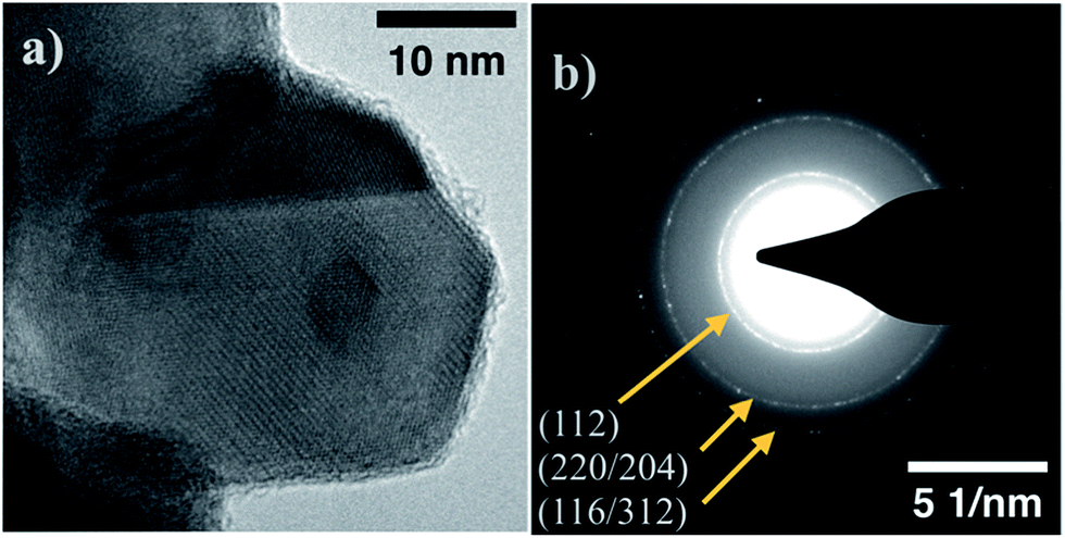 | ||
| Fig. 1 (a) TEM image of representative CZTS nanoparticle sample. (b) Selected Area Electron Diffraction (SAED) pattern for CZTS sample, fringes aligning with kesterite CZTS labeled. | ||
The composition of the material is easily tuneable by adjusting the relative precursor ratios in the precursor solution. Fig. 2 shows the elemental composition (acquired by SEM/EDS) for a series of samples that were made with the specific intent of controlling the Cu/Zn atomic ratio. Past studies have shown that the ability to control CZTS stoichiometry to be slightly copper-poor and zinc-rich increases the performance of photovoltaics.35,36 Specifically, the best-performing devices have a Cu/Zn atomic ratio of around 1.84 (the ratio of NP5 in Fig. 2 is 1.8) where in stoichiometric CZTS the ratio would be 2 (shaded bars in Fig. 2). From Fig. 2, the samples are observed to be consistently sulfur-deficient by about 5 atomic percent. This is inconsequential because the material is eventually annealed in an excess sulfur environment, so the sulfur content is recovered in the ultimate thin films.
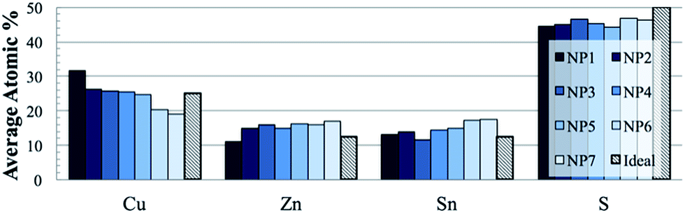 | ||
| Fig. 2 Bar graph showing relative atomic concentrations of Cu, Zn, Sn, and S in a series of nanoparticle samples exhibiting compositional control of the product. Shaded bars correspond to stoichiometric Cu2ZnSnS4. Data acquired by SEM/EDS. | ||
As alluded to in the Methods section, the particles are observed to be embedded in an amorphous matrix (Fig. S2†) when the spray pyrolysis system is operated at higher temperatures (>800 °C). This is the result of the decomposition of the dedc–precursor complexes and of solvent decomposition as well.37 This calls into question how “carbon-free” the surface of these CZTS particles are. However, XPS analysis confirms that for the particles shown in Fig. 1, which have been produced at sufficiently low temperature to avoid the carbon contamination, the surface has a very low carbon content, ∼0.15 atomic percent (Fig. S4a†).
Attempts at making uniform, large-grain CZTS thin films based on the powder as produced from the aerosol spray pyrolysis reactor with no post-treatment other than solvent-rinsing and centrifuging have proven unsuccessful. A typical result is shown in Fig. 3. There is some grain growth in the bulk of the film, the uniform-looking grains in the background have an average size of 230 ± 50 nm. Further, the background layer is porous and thin. From a cross section SEM image, the thickness of this layer is approximated at less than 1 μm, while the initial coating before annealing had a thickness of approximately 3.5 μm. The annealed film is also non-uniform. There are sparse occurrences of very large grains segregated above the bulk of the film. Volume conservation suggests that the massive reduction in the thickness of the bulk of the film can be explained by material loss to these large grains that extend as high as 5 μm above the surface of the bulk film. A similar result is noted by Chernomordik et al. in the sintering of ligand-capped pure sulfide CZTS nanoparticle films.38
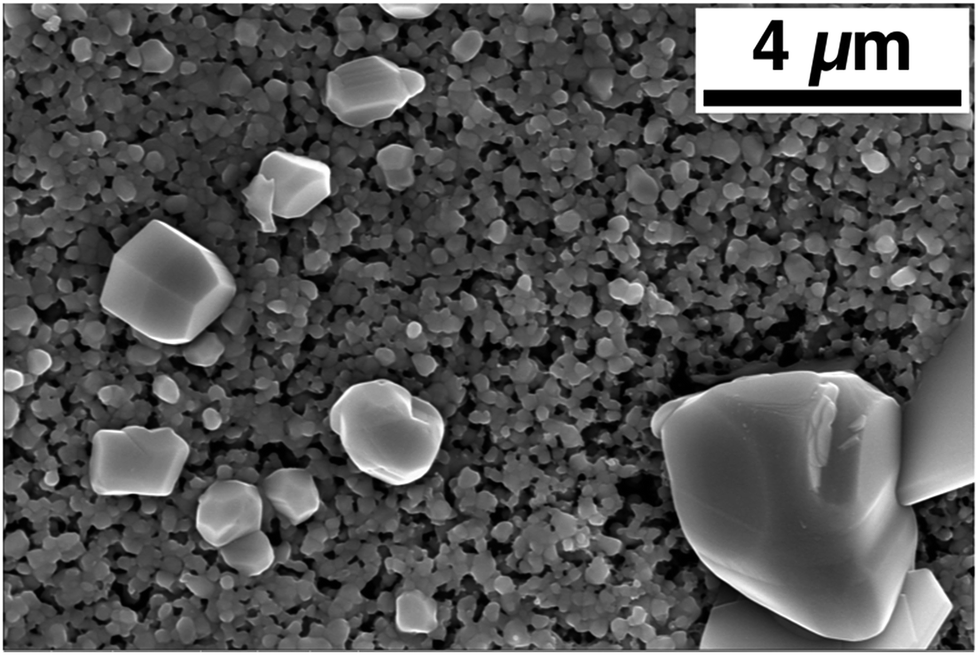 | ||
| Fig. 3 Top-down SEM image of sulfur-annealed CZTS nanoparticles with no post-synthesis treatment. | ||
In order to investigate the role of surface chemistry on the sintering kinetics of CZTS nanoparticles, we have tested a very simple air-annealing process. This was originally motivated by the idea that such a process would remove any residual trace amount of carbon contamination, due to either solvent residue or unreacted precursor not removed by the cleaning procedure. The annealing temperature range is between 200 and 300 °C. Fig. 4 shows the effect of the air annealing process on particle morphology for two different temperatures: 225 °C and 300 °C. At 225 °C (Fig. 4B), there is a clear modification to the particle surface, and at 300 °C (Fig. 4C), the formation of a thin amorphous layer is thicker (∼1.5 nm) and clearly distinguishable. It should be stressed that the bulk of the material retains the apparent phase-pure CZTS character, as confirmed by XRD and Raman spectroscopy (Fig. S5†).
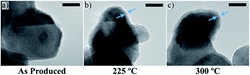 | ||
| Fig. 4 TEM images of CZTS nanoparticles as-produced from the spray pyrolysis reactor (a), after annealing in air at 225 °C (b), and after annealing in air at 300 °C (c). Arrows indicate presence of amorphous oxide layer after air annealing. Scale bar is 10 nm. | ||
XPS characterization confirms that the amorphous layer on the surface of the particles is an oxide primarily comprised of tin and zinc cations (Fig. S4†). From Fig. S4,† it is also interesting to note that the surface of air annealed particles tends to be more rich in tin and zinc, and consequently more copper-poor, compared to the surface of particles that have not been air annealed. SEM/EDS measurements indicate that the loss of copper is restricted to the particle surface; the composition of the bulk powder remains the same within uncertainty of the measurement. Other groups have observed similar behavior in the CZTS layer after annealing CZTS-based PV devices in air.39–42 Using Auger Nanoprobe Spectroscopy, Sardashti et al. characterized the formation of these copper-depleted, SnOx-enriched surfaces in the absorber layer after air-annealing a CZTSSe-based PV.39 The absence of copper at the particle surfaces may be attributed to the formation of CuSO4, which is volatile at temperatures much lower than the air annealing temperature.43 Copper sulfate has a relatively low heat of formation,44 and the corresponding zinc and tin sulfates are much less likely to form – the respective heats of formation are roughly 5 and 10 times greater in magnitude than that for copper sulfate.44,45
These air annealed CZTS particle samples are then coated, pressed, and annealed according to the exact same procedure used for the non-air annealed particles. The as-produced powder-derived samples appear to be morphologically similar to that seen in Fig. 3 – large CZTS grains are formed sparsely and on the surface of a uniform-but-porous smaller grain layer. The resulting films derived from the air annealed powder are starkly contrasting, however. The film, as determined from SEM, consists of uniform, large grain CZTS (Fig. 5e–g). The average grain size for the sample derived from powder annealed in air at 225 °C is 1.8 ± 0.5 μm. The powder annealed at 225 °C consistently gives the most uniform and least porous film, though similarly uniform grain growth is observed for all films derived from powder annealed in air between 200 and 300 °C. The air annealed sample exhibits uniform large grain morphology on a large scale (Fig. 5e) relative to the non-air annealed counterpart (Fig. 5a).
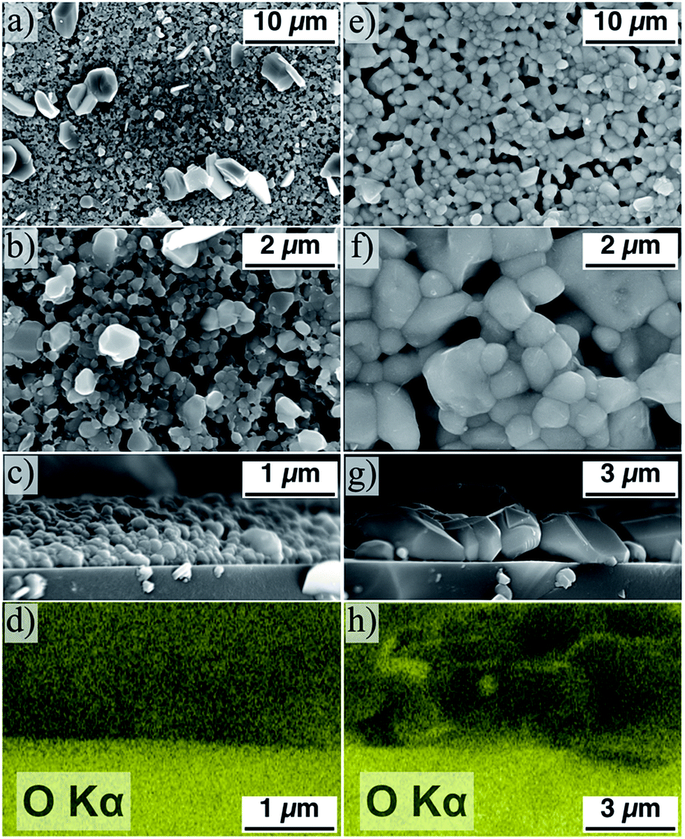 | ||
| Fig. 5 Top down and cross section SEM images of films derived from as-produced CZTS nanoparticles (a–c) and nanoparticles annealed in air at 225 °C (e–g). (d) and (h) are EDS maps of oxygen content in images (c) and (g) respectively. | ||
A further notable result is observed in Fig. 5g – the large grains of CZTS span the thickness of the film (∼2 μm) with no carbon-rich fine-grain layer between the film and the substrate. Typically in related work, CZTS nanoparticles are synthesized via a hot-injection method, and consequently are covered at the surface with organic ligands. These ligands result in the aforementioned carbon-rich fine-grain layer sandwiched between the bulk of the film and the substrate.1,46–49 Huang et al. have demonstrated a method to eliminate this fine-grain layer by using ligand-free CZTS nanoparticles synthesized by hot-injection in a formamide solvent system and maximizing the packing density of the nanoparticle coating before annealing.23 The samples shown in Fig. 5 implies that a similar result can be achieved by an alternative mean – by starting with ligand-free CZTS nanoparticles and performing a 30 minute anneal in atmosphere at moderate temperature.
Intuitively, the introduction of oxygen into the material may adversely affect charge transport in the film by introducing poorly conducting phases into the structure. In Fig. 5h, the oxygen in the system appears to aggregate at the surfaces of the grains and not in the bulk. Further characterization is necessary to investigate the role of such oxide segregations on the electronic properties of the films. Such a study goes beyond the scope of this report. Nevertheless, the conclusion from a recent study by Sardashti et al. is that the presence of tin-oxide phases and copper-depletion at the surface of the grains in a CZTS thin film act as a passivating layer, inhibiting charge recombination at grain boundaries.39 Air annealing CZTS/CZTSSe-based PVs after production is now commonly applied to enhance device efficiency by this passivation mechanism.40
Structurally, both of the annealed films in Fig. 5 appear to be phase-pure CZTS (Fig. 6). Comparisons in diffraction and Raman spectra between the air annealed powder-derived sample and the as-produced powder-derived sample show minimal bulk-phase variability. In Fig. 6a, the diffraction peaks between the two samples align, with the 112 peak strongest at 28.4° aligning well with CZTS standards.34 The difference is that the air annealed sample exhibits sharper peaks, to be expected after observing the morphology in SEM. Scherrer peak analysis of the respective 112 peaks in Fig. 6a yields an approximate average crystallite size of 130 nm for the “AirA (225 °C)” sample and 77 nm for the “As Produced” sample. In Raman (Fig. 6b), the spectra are effectively identical, with both samples exhibiting CZTS peaks at ∼286 and ∼336 cm−1.34
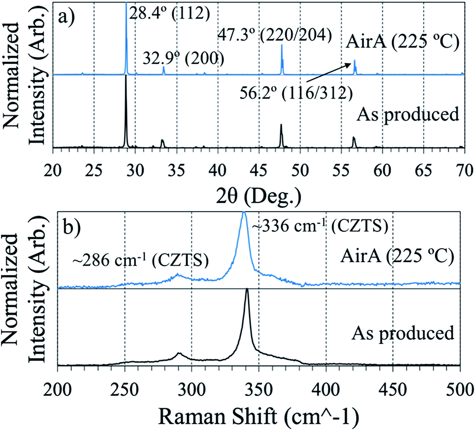 | ||
| Fig. 6 XRD (a) and Raman (b) spectra comparing air annealed powder-derived CZTS thin films to as-produced powder-derived films. Each spectrum is normalized to itself. | ||
It is crucial to apply both Raman and XRD to determine the phase of a CZTS film. Diffraction alone is insufficient due to the near perfect overlap of kesterite CZTS with its potential segregate-phases ZnS and Cu2SnS3.34 Using the same collection conditions for Raman spectroscopy outlined in the Methods section here, we have observed signatures of these segregating phases independent of the primary CZTS resonance at 336 cm−1.
It must also be noted that apparent bulk phase purity is not necessarily indicative of an entirely phase pure sample. A recent study by Alvarez et al. used Raman microprobe spectroscopy to identify structural and compositional inhomogeneity that exists from grain-to-grain in a CZTS film that appears structurally phase pure and compositionally near-stoichiometric using the conventional characterization strategy.50 The samples examined in this study were synthesized by sulfurizing a stack of sputtered Cu, Zn, and Sn metal-layers using the same technique detailed in the methods section, but for an eight-hour duration rather than the one-hour used here for nanoparticle sintering.
In the present study, after quantifying the composition of different spots in the two films obtained without and with the nanoparticle air annealing step (Fig. 7a and b respectively), it is apparent that the same localized compositional variability found by Alvarez et al. exists in the films analyzed in this study. The table beneath Fig. 7a clearly shows a variability in the metal content between the small grains and the segregated large grains. The large grains each have a relatively higher tin and copper content, as evidenced by the decrease in the Zn/Sn ratio from spots 1 and 2 to spots 3, 4, and 5. The copper content is highly variable, with a large increase between the spots 1, 2, and 3, 4, and 5. In the air annealed nanoparticle-derived film (Fig. 7b), there is still variability from grain-to-grain as well. The small grain in spot 2 appears to be more tin- and copper-poor than the others surveyed, matching the trend between the large and small grains in Fig. 7a. However, the sample in Fig. 7b shows a consistently higher tin content relative to zinc.
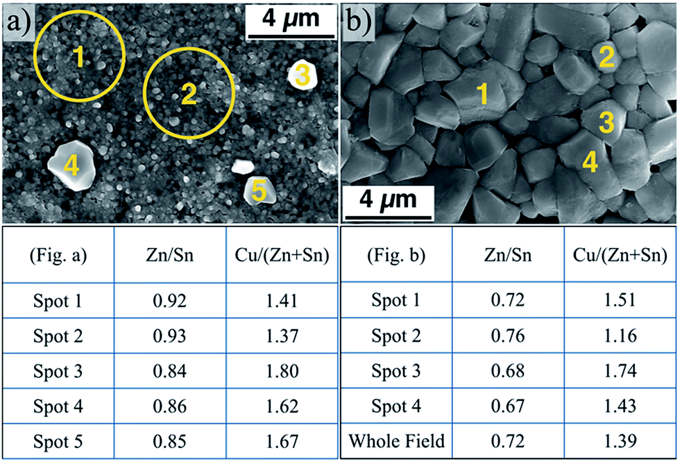 | ||
| Fig. 7 Top down SEM images of as-produced CZTS powder-derived film (a) and air annealed CZTS powder-derived film (b) with different spots showing locations of EDS elemental quantification (in atomic %). Each number corresponds to the underlying grain and the respective spot in the table below, where Cu, Zn, and Sn are quantified with respect to each other. In the table under (b), “Whole Field” refers to elemental quantification of the entire image. | ||
In addition to these observations, we have compared the average (measured at low magnification to include a large number of grains) amount of tin in several sulfurized CZTS thin films (Fig. 8). We have found consistently higher tin content in films produced using the air annealed powder.
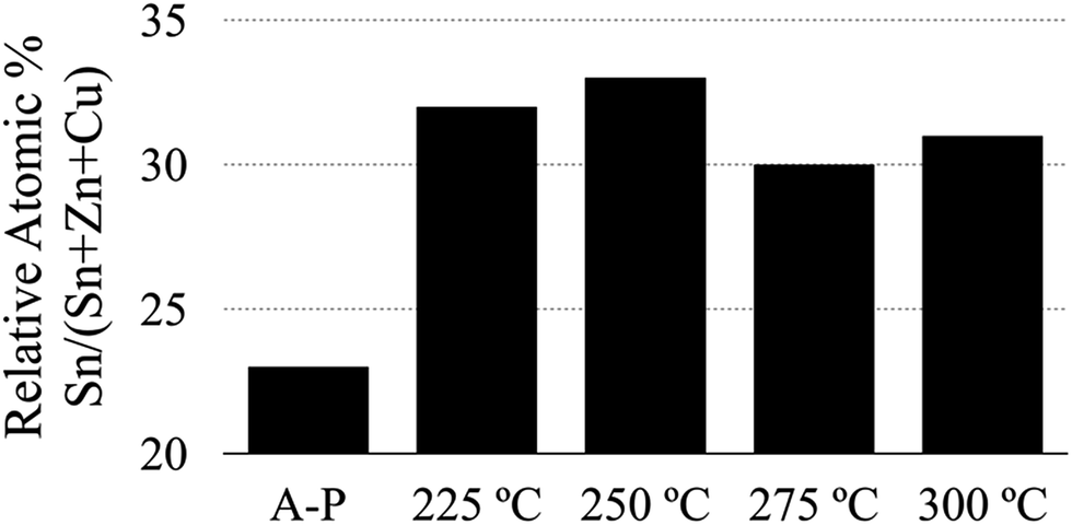 | ||
| Fig. 8 Comparison of tin content relative to all metals in annealed CZTS thin films. The bars represent as-produced (A-P), and different temperature air annealed CZTS nanoparticle-derived films. | ||
To summarize, the elemental analysis data shown in Fig. 7 and 8 give some insight into the grain growth mechanics for the CZTS material system and suggest that tin plays a crucial role in the kinetics of grain growth in CZTS thin films. This information, after comparing the morphologies and compositions between large and small grains (Fig. 7) and after comparing the composition of films realized from particles with and without an oxide shell, supports the conclusion that the amorphous oxide layer formed during the air annealing process (Fig. 4) acts as a diffusion barrier that helps in retaining volatile phases during the high temperature sulfurization step.
Conclusions
We have presented a novel approach for the synthesis of CZTS nanoparticles based on the aerosol spray pyrolysis of a mixture of Cu-, Zn-, and Sn-dedc precursors. This technique enables the continuous production of CZTS nanoparticles with precise control of their stoichiometry. Under optimal process conditions, the particle surface is effectively carbon-free, as confirmed by XPS analysis. Without further post-processing, these CZTS nanoparticles do not yield uniform large grain thin films upon sulfurization. However, by introducing a mild annealing step in air it is possible to grow a thin amorphous oxide layer on the surface of the CZTS nanoparticles without compromising the kesterite-CZTS crystal structure. Such particles lead to films with uniformly large grains after sulfurization. We have found that the oxygen introduced into the system appears to aggregate at the surface of the grains in the film.In addition, careful SEM/EDS analysis indicates that: (a) in films obtained from particles that are not annealed in air (without an oxide layer) few large grains can be found, and such grains are consistently more tin-rich than the majority of the small grains that compose the film, and (b) films obtained from particles that are annealed in air (with an oxide layer) are consistently more tin-rich than films obtained from particles without an oxide layer. These observations imply that the retention of volatile tin sulfide phases, aided by the presence of a surface-oxide layer, plays an important role in the sintering of CZTS nanoparticle films.
Acknowledgements
This work has been partially supported by the National Science Foundation under award number 1545852 (PIRE). L. Mangolini acknowledges the support of the National Science Foundation under award number 1351386 (CAREER). Raman and XRD were performed at the Analytical Chemistry Instrumentation Facility (ACIF) at UC Riverside. SEM, EDS, and TEM were performed at the Central Facility for Advanced Microscopy and Microanalysis (CFAMM) at UC Riverside. We acknowledge the National Science Foundation under grant DMR-0958796 for support with the XPS characterization. We thank Alejandro Alvarez for insightful discussion.References
- Q. Guo, H. W. Hillhouse and R. Agrawal, J. Am. Chem. Soc., 2009, 131(33), 11672–11673 CrossRef CAS PubMed.
- T. K. Todorov, K. B. Reuter and D. B. Mitzi, Adv. Mater., 2010, 22(20), E156–E159 CrossRef CAS PubMed.
- Q. Guo, G. M. Ford, Y. C. Yang, B. C. Walker, E. A. Stach, H. W. Hillhouse and R. Agrawal, J. Am. Chem. Soc., 2010, 132(49), 17384–17386 CrossRef CAS PubMed.
- D. B. Mitzi, O. Gunawan, T. K. Todorov, K. Wang and S. Guha, Special issue: Thin Film and Nanostructured Solar Cells, 2011, vol. 95, 6, pp. 1421–1436 Search PubMed.
- W. Wang, M. T. Winkler, O. Gunawan, T. Gokmen, T. K. Todorov, Y. Zhu and D. B. Mitzi, Adv. Energy Mater., 2014, 4(7), 1301465 CrossRef.
- W. Shockley and H. J. Queisser, J. Appl. Phys., 1961, 32(3), 510–519 CrossRef CAS.
- X. Liu, Y. Feng, H. Cui, F. Liu, X. Hao, G. Conibeer, D. Mitzi and M. Green, Progress in Photovoltaics: Research and Applications, 2016, 24, 879–898 CrossRef.
- B. D. Chernomordik, A. E. Béland, N. D. Trejo, A. A. Gunawan, D. D. Deng, K. A. Mkhoyan and E. S. Aydil, J. Mater. Chem. A, 2014, 2(27), 10389–10395 CAS.
- T. Kameyama, T. Osaki, K. Okazaki, T. Shibayama, A. Kudo, S. Kuwabata and T. Torimoto, J. Mater. Chem., 2010, 20(25), 5319 RSC.
- W. C. Liu, B. L. Guo, X. S. Wu, F. M. Zhang, C. L. Mak and K. H. Wong, J. Mater. Chem. A, 2013, 1(9), 3182–3186 CAS.
- K. Rawat, H. J. Kim and P. K. Shishodia, Mater. Res. Bull., 2016, 77, 84–90 CrossRef CAS.
- M. Cao and Y. Shen, J. Cryst. Growth, 2011, 318(1), 1117–1120 CrossRef CAS.
- B. Flynn, W. Wang, C. Chang and G. S. Herman, Phys. Status Solidi A, 2012, 209(11), 2186–2194 CrossRef CAS.
- S. W. Shin, J. H. Han, Y. C. Park, G. L. Agawane, C. H. Jeong, J. H. Yun, A. V. Moholkar, J. Y. Lee and J. H. Kim, J. Mater. Chem., 2012, 22(40), 21727–21732 RSC.
- T. Nakada, D. Iga, H. Ohbo and A. Kunioka, Jpn. J. Appl. Phys., Part 1, 1997, 36(1–2), 732–737 CrossRef CAS.
- A. Rockett, Thin Solid Films, 2004, 480–481, 2–7 Search PubMed.
- T. Prabhakar and N. Jampana, Sol. Energy Mater. Sol. Cells, 2011, 95(3), 1001–1004 CrossRef CAS.
- W. M. H. Oo, J. L. Johnson, A. Bhatia, E. A. Lund, M. M. Nowell and M. A. Scarpulla, J. Electron. Mater., 2011, 40(11), 2214–2221 CrossRef.
- J. V. Li, D. Kuciauskas, M. R. Young and I. L. Repins, Appl. Phys. Lett., 2013, 102(16), 163905 CrossRef.
- M. Johnson, S. V. Baryshev, E. Thimsen, M. Manno, X. Zhang, I. V. Veryovkin, C. Leighton and E. S. Aydil, Energy Environ. Sci., 2014, 7(6), 1931–1938 CAS.
- T. R. Martin, J. K. Katahara, C. N. Bucherl, B. W. Krueger, H. W. Hillhouse and C. K. Luscombe, Chem. Mater., 2016, 28(1), 135–145 CrossRef CAS.
- T. J. Huang, X. Yin, C. Tang, G. Qi and H. Gong, ChemSusChem, 2016, 9(9), 1032–1041 CrossRef CAS PubMed.
- T. J. Huang, X. Yin, C. Tang, G. Qi and H. Gong, J. Mater. Chem. A, 2015, 3(34), 17788–17796 CAS.
- A. Weber, R. Mainz and H. W. Schock, J. Appl. Phys., 2010, 107(1), 013516 CrossRef.
- J. J. Scragg, T. Ericson, T. Kubart, M. Edoff and C. Platzer-Björkman, Chem. Mater., 2011, 23(20), 4625–4633 CrossRef CAS.
- M. C. Johnson, C. Wrasman, X. Zhang, M. Manno, C. Leighton and E. S. Aydil, Chem. Mater., 2015, 27(7), 2507–2514 CrossRef CAS.
- A. Redinger, D. M. Berg, P. J. Dale and S. Siebentritt, J. Am. Chem. Soc., 2011, 133(10), 3320–3323 CrossRef CAS PubMed.
- S. Liu, H. Zhang and M. T. Swihart, Nanotechnology, 2009, 20(23), 235603 CrossRef PubMed.
- A. Khare, A. W. Willis, L. M. Ammerman, D. J. Norris and E. S. Aydil, Chem. Commun., 2011, 47(42), 11721–11723 RSC.
- B. A. Williams, A. Mahajan, M. A. Smeaton, C. S. Holgate, E. S. Aydil and L. F. Francis, ACS Appl. Mater. Interfaces, 2015, 7(21), 11526–11535 CAS.
- A. Alvarez, S. Exarhos and L. Mangolini, Mater. Lett., 2016, 165, 41–44 CrossRef CAS.
- T. P. Dhakal, C. Peng, R. R. Tobias, R. Dasharathy and C. R. Westgate, Sol. Energy, 2014, 100, 23–30 CrossRef CAS.
- S. Hong and C. Kim, Mol. Cryst. Liq. Cryst., 2014, 602(1), 134–143 CrossRef CAS.
- A. J. Cheng, M. Manno, A. Khare, C. Leighton, S. A. Campbell and E. S. Aydil, J. Vac. Sci. Technol., A, 2011, 29(5), 051203 Search PubMed.
- K. Tanaka, Y. Fukui, N. Moritake and H. Uchiki, Sol. Energy Mater. Sol. Cells, 2011, 95(3), 838–842 CrossRef CAS.
- B. Shin, O. Gunawan, Y. Zhu, N. A. Bojarczuk, S. J. Chey and S. Guha, Progress in Photovoltaics: Research and Applications, 2013, 21(1), 72–76 CrossRef CAS.
- B. Ludolph and M. A. Malik, Chem. Commun., 1998,(17), 1849–1850 RSC.
- B. D. Chernomordik, A. E. Béland, D. D. Deng, L. F. Francis and E. S. Aydil, Chem. Mater., 2014, 26(10), 3191–3201 CrossRef CAS.
- K. Sardashti, R. Haight, T. Gokmen, W. Wang, L. Y. Chang, D. B. Mitzi and A. C. Kummel, Adv. Energy Mater., 2015, 5(10), 1402180 CrossRef.
- R. Haight, X. Shao, W. Wang and D. B. Mitzi, Appl. Phys. Lett., 2014, 104, 033902 CrossRef.
- S. Chen, X. G. Gong, A. Walsh and S. Wei, Appl. Phys. Lett., 2010, 96, 021902 CrossRef.
- A. Ennaoui, M. Lux-Steiner, A. Weber, D. Abou-Ras, I. Kötschau, H.-W. Schock, R. Schurr, A. Hölzing, S. Jost, R. Hock, T. Voß, J. Shulze and A. Kirbs, Thin Solid Films, 2009, 517, 2511–2514 CrossRef CAS.
- P. E. Liley, G. H. Thomson, D. G. Friend, T. E. Daubert and E. Buck, Physical and Chemical Data, Section 2, The McGraw-Hill Companies, Inc., 1999 Search PubMed.
- T. S. Logan, J. Chem. Educ., 1958, 35(3), 148 CrossRef.
- H. Gamsjäger, T. Gajda, J. Sangster, S. K. Saxena and W. Voigt, Chemical Thermodynamics of Tin, Organization for Economic Co-Operation and Development, 2012 Search PubMed.
- C. J. Hages, M. J. Koeper, C. K. Miskin, K. W. Brew and R. Agrawal, Chem. Mater., 2016, 28(21), 7703–7714 CrossRef CAS.
- X. Liu, J. Huang, F. Zhou, F. Liu, K. Sun, C. Yan, J. A. Stride and X. Hao, Chem. Mater., 2016, 28(11), 3649–3658 CrossRef CAS.
- J. van Embden, A. S. R. Chesman, E. D. Gaspera, N. W. Duffy, S. E. Watkins and J. J. Jasieniak, J. Am. Chem. Soc., 2014, 136(14), 5237–5240 CrossRef CAS PubMed.
- H. Zhou, T. B. Song, W. C. Hsu, S. Luo, S. Ye, H. S. Duan, C. J. Hsu, W. Yang and Y. Yang, J. Am. Chem. Soc., 2013, 135(43), 15998–16001 CrossRef CAS PubMed.
- A. Alvarez-Barragan, H. Malekpour, S. Exarhos, A. A. Balandin and L. Mangolini, ACS Appl. Mater. Interfaces, 2016, 8(35), 22971–22976 CAS.
Footnote |
| † Electronic supplementary information (ESI) available: Details regarding the experimental apparatus, further CZTS nanoparticle characterization (abnormal production and particle size analysis), XPS characterization comparing air annealed and as-produced CZTS nanoparticles, and structural (XRD and Raman) characterization of air annealed and as-produced CZTS nanoparticles. See DOI: 10.1039/c7ra04128d |
| This journal is © The Royal Society of Chemistry 2017 |