
 Open Access Article
 This Open Access Article is licensed under a
 Creative Commons Attribution 3.0 Unported Licence
Photoconductivity of CaH2-reduced BaSnO3 thin films
C. W. Zhao,
B. C. Luo * and
C. L. Chen
* and
C. L. Chen
Key Laboratory of Space Applied Physics and Chemistry, Ministry of Education, School of Science, Northwestern Polytechnical University, Xi'an 710072, China. E-mail: luobingcheng@nwpu.edu.cn
First published on 3rd April 2017
Abstract
Incorporation of foreign chemical elements in oxides can significantly alter their optoelectronic performances, and thus it is widely used to seek new transparent conductive oxides. Chemical-doping BaSnO3 systems, like La-doped BaSnO3, are of increasing interest with extremely high electrical mobility and excellent oxygen stability, exhibiting the potential application in next-generation all-perovskite optoelectronic devices. In this work, hydrogen was introduced into BaSnO3 through CaH2 reduction of BaSnO3 thin films, and the electrical properties, as well as the photo-response behavior, were investigated. Secondary ion mass spectroscopy demonstrated the uniform distribution of hydrogen within the BaSnO3 thin film. The addition of hydrogen greatly enhanced the conductivity of the BaSnO3 thin film, exhibiting a carrier concentration ∼8.04 × 1019 cm−3 and mobility ∼9.52 cm2 V−1 s−1 at 300 K, and thus resulted in a fast relaxation process in the transient photoconductivity, which was characterized by a double exponential function indicating two physical contributions.
Introduction
Complex metal oxides are particularly attractive owing to their exceedingly diverse range of physical properties such as magnetism, ferroelectricity, superconductivity, colossal magnetoresistivity, multiferroicity, transparent conductor, and so on. More importantly, these properties can be modified by various factors (e.g., strain, chemical composition, interface, orientation, external stimuli, etc.),1–17 which makes complex metal oxides appealing materials for next generation new devices. The insulator–metal transition, one of the oldest fundamental properties, is still the subject of considerable research interest. According to the famous Mott criterion,1 most insulating metal oxides could exhibit metallic conductivity above a critical carrier density nc1/3ac > 0.25, where ac = εħ2/m*e2 is the Bohr radius, ε is the dielectric constant, and m* is the effective mass of an electron, through extrinsic doping or self-doping with oxygen vacancies. More importantly, such an insulator–metal transition in wide band-gap oxides was a very viable strategy for developing transparent conductive oxide materials, which was widely realized in a number of previous studies.2–5With this said, insulating BaSnO3 (BSO) with a band gap of 3.1 eV could exhibit the metallic conductivity through chemical doping.4,8–17 Notably, La-doping BSO was recently found to possess extremely high electrical mobility (∼320 cm2 V−1 s−1) at room temperature4 and excellent oxygen stability at high temperature (∼530 °C),11 and thus has prompted interest for applications in all-perovskite optoelectronic devices and photovoltaics. Nevertheless, La-doping BSO thin film is still limited by its poor electrical mobility compared to its counterpart bulk single crystal. Considerable effort has lately been devoted to the improvement of its electrical mobility via reducing the extended defects in La-doping BSO films.18–21 Additionally, in line with the first principle calculation results,22 Niedermeier et al. experimentally demonstrated that interstitial hydrogen in BSO films could enhance the conductivity and mobility,12 whereas the effect of hydrogen substitute for the oxide site has not yet been involved.
Ongoing demand to improve the electrical mobility is the constant driving force in BSO-based thin films, but research on photo response is also interesting both for a fundamental understanding of transport properties and for the potential application in UV detectors. Very recently, Park et al.23 compared the photoconductivity of BSO thin film with that of SrTiO3 thin film, and illustrated that BSO exhibited larger persistent conductivity due to the deep level defects with large barriers for charge trapping and detrapping. This limitation may be partially fixed when hydrogen doping in BSO, because the H+/H− doping usually form a shallow donor. Consequently, we herein synthesized hydrogen doping BSO thin films with metallic conductivity through CaH2 reduction of epitaxial BSO thin films, and further investigated the photo response performances.
Experimental
The insulating epitaxial BaSnO3 (BSO) thin films of thickness ∼100 nm were deposited on (LaAlO3)0.3(SrAl0.5Ta0.5O3)0.7 (LSAT) (001) substrates in one-shot by radio-frequency (RF) magnetron sputtering technique with BSO ceramic target, as described in detail in our previous publications.24,25 Here, the LSAT substrate was chose due to its inertness against CaH2. The as-growth BSO thin film was embedded with CaH2 powder in an evacuated Pyrex tube and then the tube was sealed in a vacuum (<0.3 mTorr), which were all done under nitrogen in a glovebox. Subsequently, the tubes were annealed under optimized conditions (annealing temperature ∼630 °C and time ∼20 h) for obtaining the lowest resistivity. Finally, the films were washed with ethanol and deionized water for 2 times to remove the excess CaH2 and CaO byproduct, and then naturally dried at nitrogen-flowing environment (labeled as BSO-H). For comparison purpose, the above-mentioned processes were also done except that the films were not embedded with CaH2 powder (labeled as BSO-V).The phase structures of the films were characterized by X-ray diffraction (XRD) (PANalytical Empyrean), with Cu Kα radiation in the usual θ–2θ geometry. The valence states of O ions were checked using X-ray photoelectron spectroscopy (XPS) (ESCALAB 250) with Al Kα radiation. For excluding the effect of the top surface, the XPS probing was performed after a thin top layer (∼8 nm) of the films was removed away by Ar+ iron beam. The hydrogen content in the films was examined using secondary ion mass spectrometry (SIMS). Temperature-dependent resistivity of the films was measured along the in-plane direction by a four-probe method, while the carrier mobility and concentration were determined through Hall measurement using van der Pauw geometry.25 Two platinum electrodes were vacuum-evaporated onto the film, through which a 6487 Keithley electrometer/Tektronix 4054 was connected by a probe station for photoconductivity measurements. A Xenon lamp coupled into a grating monochromator (Oriel Cornerstone 260) was used for the light source. The light uniformly illuminated the film between the two electrodes. The photocurrent was recorded under a constant bias voltage, and normalized with the incident power at each value of the wavelength. For time dependent photoconductivity measurement, the wavelength of the illuminated light was fixed at 360 nm. All the photo response measurements were performed under vacuum environment to exclude the effect of the absorbed molecules.
Results and discussion
Fig. 1(a) presents XRD patterns of BSO-H and BSO-V thin films with a logarithmic scale. All the films show only the (00l) peaks corresponding to the substrate without any secondary phases, suggesting that the films are well (00l) oriented along the normal to the substrate. From these (00l) peaks, the out-of-plane lattice parameter was calculated to be about 0.414 and 0.417 nm for BSO-H and BSO-V thin films, respectively. The out-of-plane lattice parameter of BSO-H thin film is slightly smaller than that of BSO-V thin film. In analogy to the CaH2-reduction ATiO3 (A = Ba, Sr, Ca) thin films deposited on LSAT substrates,26 this lattice change might also be attributed to the compositional change. Previous experiment indicated that oxygen deficiency in BSO thin films could result in the expansion of the out-of-plane lattice parameter.27 Consequently, the O 1s spectra investigated by XPS analysis are plotted in Fig. 1(b). The O 1s spectrum from BSO-H thin film exhibits a symmetric peak at 529.9 eV, corresponding to the lattice oxygen (OL). However, the O 1s spectrum from BSO-V thin film are asymmetric and can be deconvoluted into two peaks at 530.0 and 531.5 eV, corresponding to the lattice oxygen (OL) and oxygen vacancies (OV), respectively.24 This result demonstrates that only the BSO-V thin film is oxygen-deficient. Consequently, if considering H− with the close ionic radius to O2−, the larger lattice parameter in BSO-V thin film is due to oxygen vacancies, and H− substitution for the O2− ( ) in BSO-H film is mostly expectable due to CaH2 reduction.
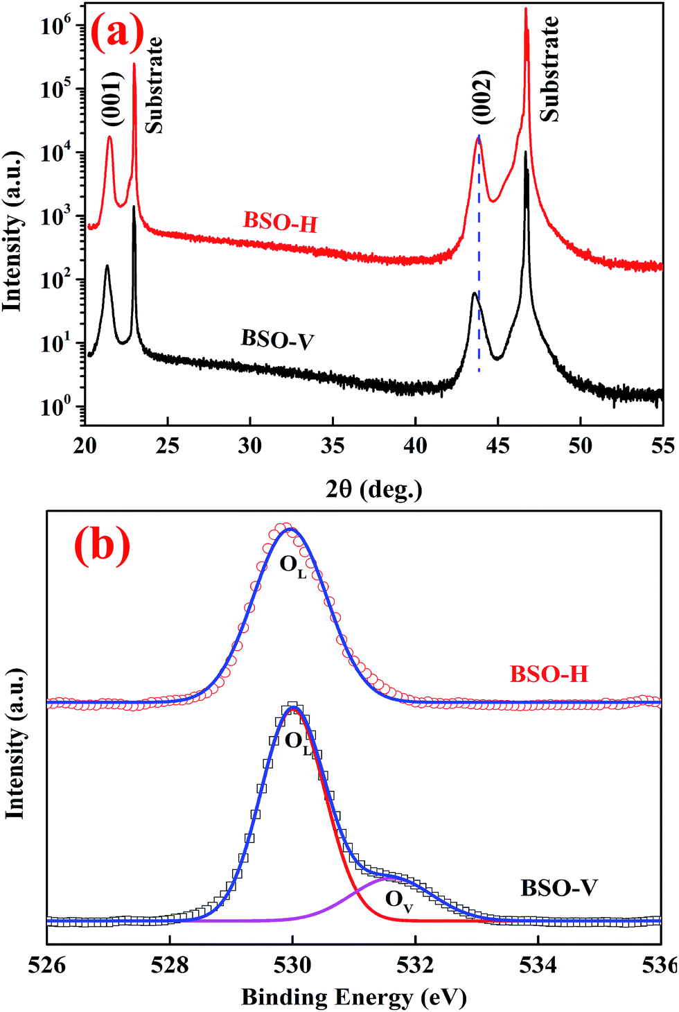 | ||
| Fig. 1 (a) XRD pattern of BSO-H and BSO-V thin films. (b) The O 1s spectra from BSO-H and BSO-V thin films, indicating lattice oxygen (OL) and oxygen vacancies (OV). | ||
To clarify whether hydrogen is incorporated into film, the SIMS depth-profiles of H ion in BSO-H and BSO-V thin films were measured, as depicted in Fig. 2. The observed intensity of the H secondary ion signal in BSO-H thin film is >2 orders of magnitude larger than that in BSO-V thin film, and the intensity over the entire depth profile is nearly constant. These data implied that H ion was basically uniform in BSO-H thin film although the precise hydrogen concentration was determined difficultly due to the absence of a hydrogen quantification standard. Generally, substitutional hydride ions ( ) and protons (
 ) may coexist in sample when reduced with CaH2. However, recent calculations suggested that CaH2 annealing process could promote formation of
  rather than
  in oxides due to lower formation energy of
  .28 Meanwhile, in recent experiment about intentional H doping in La-doping BSO thin films,12 the intensity signal of the H secondary ion decreased with thickness, and was finally similar with the background signal. Therefore, our SIMS results reflected that hydrogen species in BSO-H film were most likely trapped at oxygen sites (
 ).
).
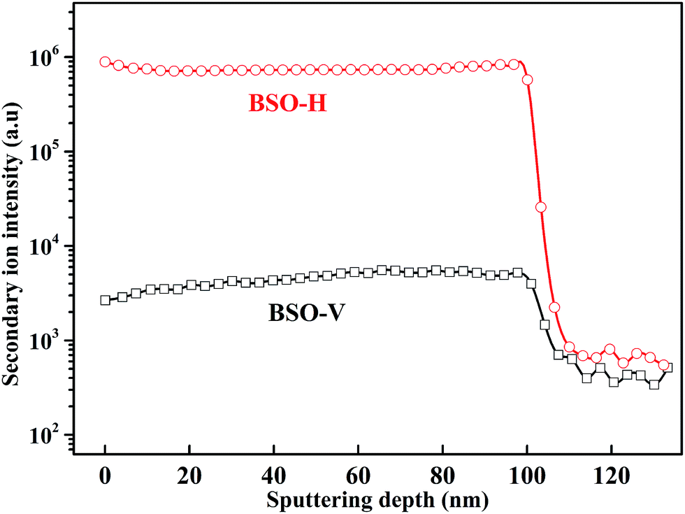 | ||
| Fig. 2 SIMS depth profile of the H secondary ion in BSO-H and BSO-V thin films. | ||
The as-grown BSO thin film was highly insulating and its resistivity was beyond the measurement limit of our equipment. Interestingly, the BSO-V thin film still behaved insulating conductivity whereas the BSO-H exhibited the metallic conductivity, as displayed in Fig. 3(a). Based on aforementioned XRD analysis, it is understandable that the resistivity of BSO-V film is smaller than that of as-grown BSO film due to oxygen vacancies. While for BSO-H thin film, it is believable that the H− charge transition level lies virtually constant at ∼4.5 eV below the vacuum level,12,29,30 and thus easily form a shallow donor inside the conduction band of BSO film, resulting in highly conductive performance. On the other hand, the electrical property of interstitial H doping BSO thin film can be reversible through high vacuum annealing (i.e., from conductor to insulator),12 whereas the BSO-H thin film is still conductive at 300 K, even annealed under high vacuum at 600 °C (see the inset of Fig. 3(a)), indicating that the primary of hydrogen species in BSO-H thin film are H−, not proton. Accordingly, replacing the oxide ions with hydride ions in BSO film could also give rise to insulator–metal transition, analogous to ATiO3 (A = Ca, Sr, Ba) thin films upon annealing with CaH2.26 Further, the temperature-dependent carrier concentration and mobility of BSO-H thin film were measured, as shown in Fig. 3(b). At 300 K, the carrier concentration and mobility are 8.04 × 1019 cm−3 and 9.52 cm2 V−1 s−1, respectively. Note that the mobility of our BSO-H thin film is still relatively low, but it is very much comparable to previous report in La-doping BSO thin film deposited on LSAT substrate,25 demonstrating H− as dopant is another advantageous choice to induce metallic conductivity for insulating BSO thin film.
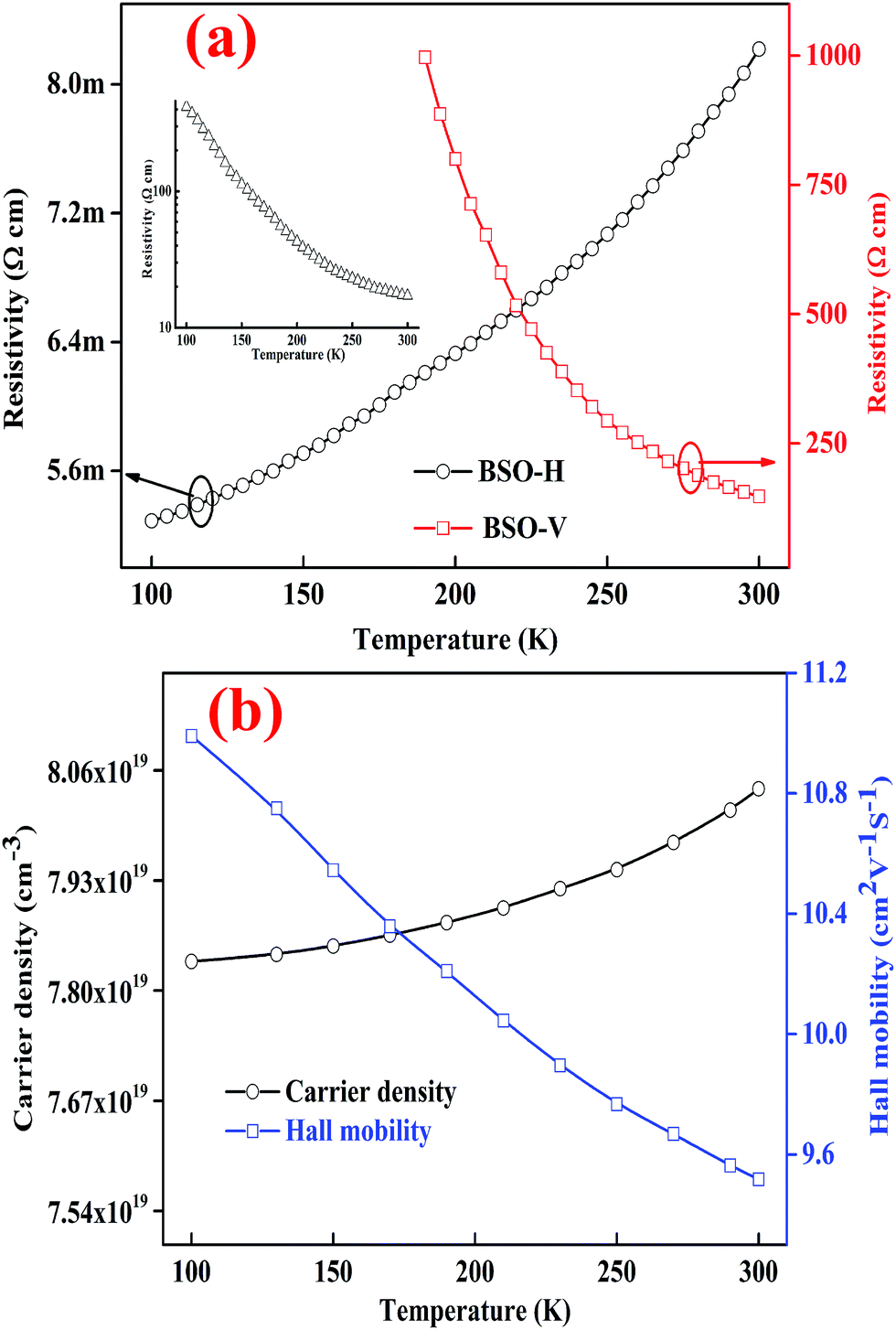 | ||
| Fig. 3 (a) Temperature-dependent resistivity of BSO-H and BSO-V thin films. Inset shows the temperature-dependent resistivity of BSO-H thin film annealed in vacuum. (b) Temperature dependence of the mobility and carrier concentration for BSO-H thin film. | ||
Fig. 4 illustrates the spectral response of the BSO-H thin film as function of wavelengths at 0.2 V and 1 V bias. Both the spectral response exhibit a sharp increase at 390 nm (∼3.18 eV), corresponding the band-to-band absorption of the BSO-H thin film. The response turned to be more prominent with the increasing voltage in the UV region, because the photo-generated carriers could migrate toward the electrodes under the external bias to form the current. With a 1 V bias, the responsivity can be above 0.8 A W−1 below the wavelength of 360 nm. Usually, BSO-based thin films were grown on lattice-mismatched substrates, leading to an inevitably high density of dislocations, which strongly weakened their electrical and photoconductive properties.23,31,32 However, the response value of our BSO-H thin film in the UV region is very much comparable to the wide band-gap oxide thin films.33 What's more, the current–voltage characteristics under different light power were measured, as shown in the inset of Fig. 4, confirming the ohmic contact between electrode and film. Meanwhile, the current increases monotonically with increasing the light power, indicating that the electron–hole pair generation is the main origin for the photo response.
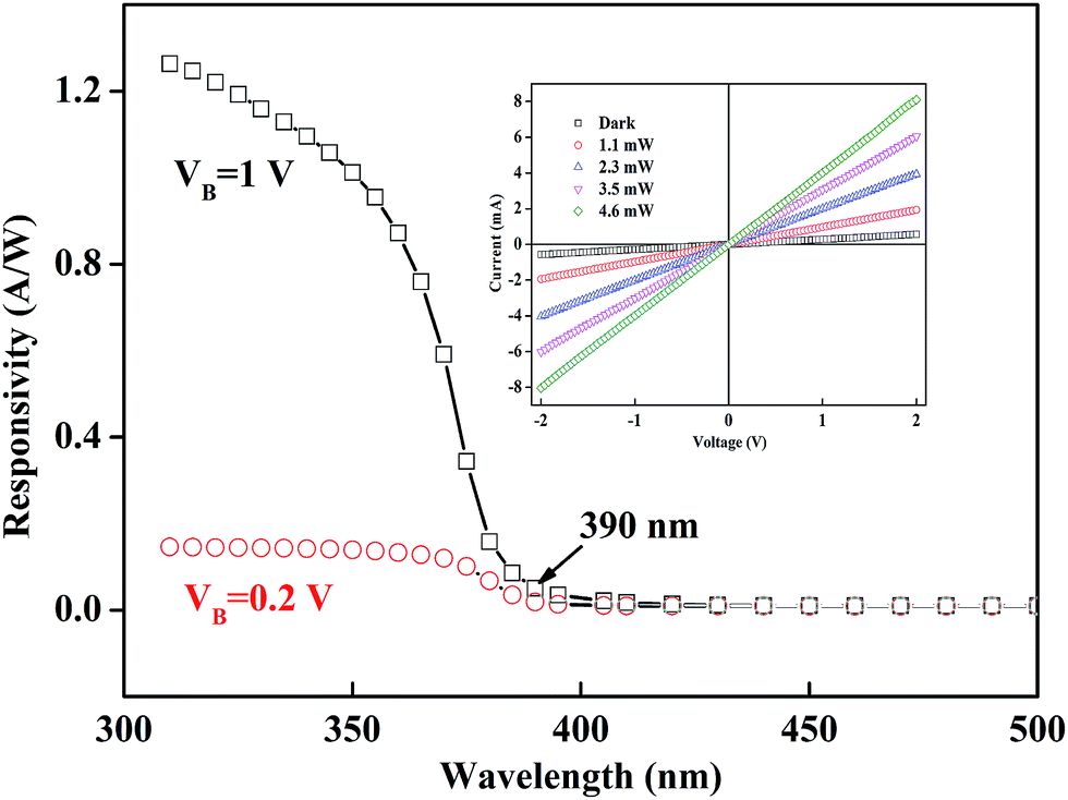 | ||
| Fig. 4 Spectral response of BSO-H thin film at 0.2 V and 1 V bias. Inset presents the current–voltage curves under illumination with different optical power. | ||
To further explore the photo response performance of BSO-H thin film, the time dependent response was subsequently investigated. Fig. 5 presents the time dependence of the resistance ratio RL/RD (RL is the resistance under illumination and RD is the dark resistance) at 100 K, 200 K and 300 K. Firstly, all the resistances rapidly decrease to the minimum values during illumination, corresponding to the band-to-band excitation, and then exhibit a long recovery process after illumination, relating with the relaxation process of carriers. Notably, the recovery process is complete in several seconds and much shorter than that had been reported on un-doped BSO thin film,23 which is mostly due to the high carrier density and mobility in BSO-H thin film.34,35 Secondly, the recovery process reflects the carrier's dynamics of recombination, and the carrier transit time (τ1) and the excess life-time of trapped carriers (τ2, τ2 > τ1) are well-known to be the main parts of the recovery time in oxide semiconductors.36 Therefore, the experimental data should be well fitted by a double exponential function37 (see red solid lines in Fig. 5), and the fitting parameters are summarized in inset of Fig. 5. At 300 K, the carrier transit time and the excess life-time of trapped carriers are 7.06 ms and 118.9 ms, respectively. Clearly, the excess lifetime of trapped carriers is the main reason for the recovery time. It has been proved in BSO-based thin films that the trapped states associated with defects including dislocations, ionized impurity, oxygen vacancies, etc.31,32 were widely existed. After illumination, some of electron–hole pairs may not recombine, and instead, may be trapped by defects. Consequently, release of these trapped carriers will have a definitive influence on the recovery process. Finally, we noticed that the variable value of resistances under illumination was almost independent of the measured temperatures. Through photo-Hall measurements, previous investigations demonstrated that the increased carrier concentration is the determination of the contribution to the photoconductivity in oxide thin films (WO3 and Ti1−xNbxO2).38,39 In present case, the short photo response time of BSO-H thin film is beyond the time resolution of our photo-Hall measurement, and thus it is hard to briefly verify that the variable resistance is due to carrier concentration or mobility or both. However, considering the weak temperature-dependent carrier concentration in BSO-H thin film (see Fig. 3(b)), it is reasonable to assume that the change of resistances under illumination is still involved with the increased carrier concentration like the Ti1−xNbxO2 thin films,39 although the deep mechanisms need to be investigated further.
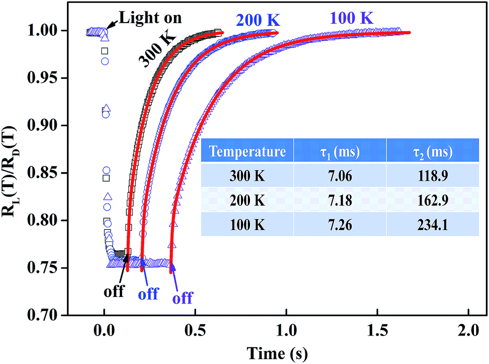 | ||
| Fig. 5 Time dependence of the resistance ratio RL/RD at different temperatures. The red solid lines are the fitting curves and the fitting parameters are given in inset. | ||
Summary
In summary, we fabricated hydrogen-doping BaSnO3 through CaH2 reduction of epitaxial BaSnO3 thin films, and mainly investigated the optoelectronic properties. XRD and SIMS measurements revealed that the hydrogen unchanged the structure of BaSnO3 thin film and uniformly existed in the film. The addition of hydrogen significantly improved the conductivity of BaSnO3 thin film, transiting from the insulator to metallic property with a carrier concentration ∼8.04 × 1019 cm−3 and mobility ∼9.52 cm2 V−1 s−1 at 300 K. Through the spectral response measurements, a wavelength cutoff at ∼3.18 eV was observed, and the responsivity could be above 0.8 A W−1 with a 1 V bias in the ultraviolet range. Additionally, hydrogen doping in BSO thin film could enhance the photoelectric response characteristic due to the high carrier density and mobility. Meanwhile, the recovery process could be analyzed by a double exponential function, indicating the influence of the carrier transit and release of trapped carriers, and simultaneously demonstrating that release of trapped carriers has a definitive role on the recovery process.Acknowledgements
This work was partly supported by National Natural Science Foundation of China (No. 51202195).References
- N. F. Mott, Rev. Mod. Phys., 1968, 40, 677 CrossRef CAS.
- T. Minami, Semicond. Sci. Technol., 2005, 20, S35 CrossRef CAS.
- J. Ravichandran, W. Siemons, H. Heijmerikx, M. Huijben, A. Majumdar and R. Ramesh, Chem. Mater., 2010, 22, 3983–3987 CrossRef CAS.
- H. J. Kim, U. Kim, T. H. Kim, J. Kim, H. M. Kim, B. G. Jeon, W. J. Lee, H. S. Mun, K. T. Hong, J. Yu, K. Char and K. H. Kim, Phys. Rev. B: Condens. Matter Mater. Phys., 2012, 86, 165205 CrossRef.
- S. C. Dixon, D. O. Scanlon, C. J. Carmalt and I. P. Parkin, J. Mater. Chem. C, 2016, 4, 6946–6961 RSC.
- K. C. Wilson, E. Manikandan, M. B. Ahamed and B. W. Mwakikunga, J. Alloys Compd., 2014, 585, 555–560 CrossRef CAS.
- E. Manikandan, V. Murugan, G. Kavitha, P. Babu and M. Maaza, Mater. Lett., 2014, 131, 225–228 CrossRef CAS.
- X. Luo, Y. S. Oh, A. Sirenko, P. Gao, T. A. Tyson, K. Char and S. W. Cheong, Appl. Phys. Lett., 2012, 100, 172112 CrossRef.
- H. F. Wang, Q. Z. Liu, F. Chen, G. Y. Gao, W. B. Wu and X. H. Chen, J. Appl. Phys., 2007, 101, 106105 CrossRef.
- U. S. Alaan, P. Shafer, A. T. N'Diaye, E. Arenholz and Y. Suzuki, Appl. Phys. Lett., 2016, 108, 042106 CrossRef.
- H. J. Kim, U. Kim, H. M. Kim, T. H. Kim, H. S. Mun, B. G. Jeon, K. T. Hong, W. J. Lee, C. Ju, K. H. Kim and K. Char, Appl. Phys. Express, 2012, 5, 061102 CrossRef.
- C. A. Niedermeier, S. Rhode, S. Fearn, K. Ide, M. A. Moram and H. Hiramatsu, Appl. Phys. Lett., 2016, 108, 172101 CrossRef.
- S. Sallis, D. O. Scanlon, S. C. Chae, N. F. Quackenbush, D. A. Fischer, J. C. Woicik, J. H. Guo, S. W. Cheong and L. F. J. Piper, Appl. Phys. Lett., 2013, 103, 042105 CrossRef.
- Q. Z. Liu, J. J. Liu, B. Li, H. Li, G. P. Zhu, K. Dai, Z. L. Liu, P. Zhang and J. M. Dai, Appl. Phys. Lett., 2012, 101, 241901 CrossRef.
- R. H. Wei, X. W. Tang, Z. Z. Hui, X. Luo, J. M. Dai, J. Yang, W. H. Song, L. Chen, X. G. Zhu, X. B. Zhu and Y. P. Sun, Appl. Phys. Lett., 2014, 106, 101906 CrossRef.
- C. Shan, T. Huang, J. Z. Zhang, M. J. Han, Y. W. Li, Z. G. Hu and J. H. Chu, J. Phys. Chem. C, 2014, 118, 6994–7001 CAS.
- S. Raghavan, T. Schumann, H. Kim, J. Y. Zhang, T. A. Cain and S. Stemmer, APL Mater., 2016, 4, 016106 CrossRef.
- P. V. Wadekar, J. Alaria, M. O'Sullivan, N. L. O. Flack, T. D. Manning, L. J. Phillips, K. Durose, O. Lozano, S. Lucas, J. B. Claridge and M. J. Rosseinsky, Appl. Phys. Lett., 2014, 105, 052104 CrossRef.
- K. Fujiwara, K. Nishihara, J. Shiogai and A. Tsukazaki, AIP Adv., 2016, 6, 085014 CrossRef.
- W. J. Lee, H. J. Kim, E. Sohn, T. H. Kim, J. Y. Park, W. Park, H. Jeong, T. Lee, J. H. Kim, K. Y. Choi and K. H. Kim, Appl. Phys. Lett., 2016, 108, 082105 CrossRef.
- S. Yu, D. Yoon and J. Son, Appl. Phys. Lett., 2016, 108, 262101 CrossRef.
- D. O. Scanlon, Phys. Rev. B: Condens. Matter Mater. Phys., 2013, 87, 161201 CrossRef.
- J. Park, U. Kim and K. Char, Appl. Phys. Lett., 2016, 108, 092106 CrossRef.
- B. C. Luo, J. Zhang, J. Wang and P. X. Ran, Ceram. Int., 2015, 41, 2668–2672 CrossRef CAS.
- B. C. Luo, X. S. Cao, K. X. Jin and C. L. Chen, Curr. Appl. Phys., 2016, 16, 20–23 CrossRef.
- T. Yajima, A. Kitada, Y. Kobayashi, T. Sakaguchi, G. Bouilly, S. Kasahara, T. Terashima, M. Takano and H. Kageyama, J. Am. Chem. Soc., 2012, 134, 8782–8785 CrossRef CAS PubMed.
- Q. Z. Liu, J. M. Dai, Y. Zhang, H. Li, B. Li, Z. L. Liu and W. Wang, J. Alloys Compd., 2016, 655, 389–394 CrossRef CAS.
- X. Liu, T. S. Bjorheim and R. Haugsrud, J. Mater. Chem. A, 2017, 5, 1050–1056 CAS.
- C. G. Van de Walle and J. Neugebauer, Nature, 2003, 423, 626 CrossRef CAS PubMed.
- S. A. Chambers, T. C. Kaspar, A. Prakash, G. Haugstad and B. Jalan, Appl. Phys. Lett., 2016, 108, 152104 CrossRef.
- H. Mun, U. Kim, H. M. Kim, C. Park, T. H. Kim, H. J. Kim, K. H. Kim and K. Char, Appl. Phys. Lett., 2013, 102, 252105 CrossRef.
- U. Kim, C. Park, T. Ha, R. Kim, H. S. Mun, H. M. Kim, H. J. Kim, T. H. Kim, N. Kim, J. Yu, K. H. Kim, J. H. Kim and K. Char, APL Mater., 2014, 2, 056107 CrossRef.
- L. J. Mandalapu, F. X. Xiu, Z. Yang and J. L. Liu, Solid-State Electron., 2007, 51, 1014–1017 CrossRef CAS.
- V. N. Smolyaninova, E. Talanova, R. Kennedy, R. M. Kolagani, M. Overby, L. Aldaco, G. Yong and K. Karki, Phys. Rev. B: Condens. Matter Mater. Phys., 2007, 76, 104423 CrossRef.
- M. Poloju, N. Jayababu, E. Manikandan and M. V. R. Reddy, J. Mater. Chem. C, 2017, 5, 2662–2668 RSC.
- J. Sun, F. J. Liu, H. Q. Huang, J. W. Zhao, Z. F. Hu, X. Q. Zhang and Y. S. Wang, Appl. Surf. Sci., 2010, 257, 921–924 CrossRef CAS.
- K. X. Jin, W. Lin, B. C. Luo and T. Wu, Sci. Rep., 2015, 5, 8778 CrossRef CAS PubMed.
- J. H. Hao, S. A. Studenikin and M. Cocivera, J. Appl. Phys., 2001, 90, 5064 CrossRef CAS.
- N. Golego, S. A. Studenikin and M. Cocivera, Phys. Rev. B: Condens. Matter Mater. Phys., 2000, 61, 8262 CrossRef CAS.
| This journal is © The Royal Society of Chemistry 2017 |