
 Open Access Article
 This Open Access Article is licensed under a
 Creative Commons Attribution 3.0 Unported Licence
van der Waals epitaxy of large-area continuous ReS2 films on mica substrate†
Jing-Kai Qinac,
Wen-Zhu Shaoa,
Yang Liab,
Cheng-Yan Xu *abc,
Dan-Dan Renac,
Xiao-Guo Songb and
Liang Zhen*ac
*abc,
Dan-Dan Renac,
Xiao-Guo Songb and
Liang Zhen*ac
aSchool of Materials Science and Engineering, Harbin Institute of Technology, Harbin 150001, China. E-mail: cy_xu@hit.edu.cn; lzhen@hit.edu.cn
bShandong Provincial Key Lab of Special Welding Technology, Harbin Institute of Technology at Weihai, Weihai 264209, China
cMOE Key Laboratory of Micro-Systems and Micro-Structures Manufacturing, Harbin Institute of Technology, Harbin 150080, China
First published on 3rd May 2017
Abstract
Rhenium disulfide (ReS2) has attracted scientists' attention for its unique physical properties and potential applications in high-efficiency photodetector devices. Although lots of works have been done to obtain high-quality ReS2 nanoflakes, in-plane uniform growth is still challenging due to its unique decoupling property between layers. In this work, we successfully realized the epitaxial growth of continuous monolayer ReS2 films on mica substrate by chemical vapour deposition (CVD). By prolonging the growth time, continuous multilayer ReS2 films can also be obtained. The growth mechanism of ReS2 films is proposed based on Stranski–Krastanov theory. Filed effect transistors (FETs) based on multilayer ReS2 films exhibit typical n-type semiconducting behaviour with a carrier density of 0.27 cm2 V−1 s−1 and ON/OFF ratio of about 4 × 10³. The photoresponsivity of the phototransistor could reach up to 0.98 A W−1 with a light intensity of 0.56 mW cm−2, suggesting that ReS2 is a promising material for electronic and optoelectronic applications.
Introduction
Transition metal dichalcogenides (TMDs), two-dimensional materials with tunable bandgaps, have attracted extensive attention in recent years. Their suitable bandgaps ranging from 1–3 eV make them highly promising to fabricate nanoscale electronic and optoelectronic devices.1–7 Most TMDs undergo a crossover of their bandgap from direct to indirect as the number of layers increases, which means that monolayers with a direct bandgap could absorb and emit light more efficiently. This transition can be attributed to a strong interlayer coupling and confinement effect between layers in the stacking direction.8–10 Recently, rhenium disulfide (ReS2) has attracted scientists' attention due its distinct properties, such as interlayer decoupling effect and anisotropic electronic properties.11–13 Based on previous reports, the bandgap of ReS2 remains direct with layer increase, which means that the interlayer coupling in ReS2 is much weaker than other two-dimensional materials.14 This property makes ReS2 an ideal candidate to fabricate novel devices irrespective to the thickness. Additionally, the distorted octahedral (1T) phase of ReS2 could cause a serious symmetry splitting, leading to an anisotropic optical and electrical properties along in-plane directions.15,16Mechanical exfoliation is a typical method to obtain highly quality nanoflakes.17–19 However, the obtained mono- or few-layer ReS2 are always very small, which make them difficult to fabricate nanoscale devices. Chemical vapor deposition (CVD) is an efficient way to achieve large area monolayer TMDs films.20–22 K. Keyshar et al.23 first obtained monolayer ReS2 flakes using CVD method under relative low temperature (400–500 °C) with NH4ReO4 as Re resource, however, the synthesized monolayers have high level of vacancies due to insufficient reaction under relatively low temperature. He et al.24 achieved highly crystallized pyramid-like few-layer ReS2 flakes with Re powder as source, but the growth rate was hindered due to the high melting point of Re metal. The strong interlayer decoupling effect of ReS2 makes its out-of-plane growth predominant, which is very different from other TMDs such as MoS2 and WSe2. Certain substrates with low surface energy could facilitate the atoms migration along in-plane directions, and would be helpful to obtain uniform films with very flat surface.25–27 For example, F. Cui et al.25 realized epitaxial growth of ReS2 films on mica substrate. Te powder was used as catalyst, which could form the low melting-temperature Te–Re binary eutectic with Re metal. By this way, the growth efficiency of ReS2 can be significantly improved. Besides, the atomically smooth and chemical inert surface of mica could also facilitate the atoms migration on surface, which makes the in-plane growth of ReS2 possible. Although some work has been done, the growth of large-area continuous ReS2 films has not even been reported.
In this study, we successfully prepared large-area continuous ReS2 films by van der Waals epitaxy on mica substrate, and we also explicitly analyzed the growth mechanism based on Stranski–Krastanov theory. Large area monolayer ReS2 films with thickness of 0.8 nm can be prepared. Continuous multilayer ReS2 films were also obtained by prolonging the growth time. Furthermore, we fabricated field effect transistor (FETs) based on multilayer ReS2 films and evaluated its electrical and optoelectronic properties. Our work provides a new approach to obtain large-area continuous ReS2 films and it would be helpful to pave the way for widespread applications of ReS2.
Experimental
Materials preparation
ReS2 films were obtained using chemical vapor deposition (CVD). Fresh fluorophlogopite mica [KMg3(AlSi3O10)F2] was used as epitaxy substrate, since it could provide an atomically smooth and chemically inert surface for atoms in-plane diffusion.26,27 In this work, we use Re metal power and Re2O7 as precursors. Re2O7 volatilizes rapidly under temperature above 300 °C,28 and the partially sulfurized Re2O7 could absorb on the substrate surface, which provides abundant nucleation sites for following ReS2 growth. As the temperature goes up, ReS2 layers starts to form and expand with incoming Re and S atoms. With this method, continuous ReS2 films are obtained under reaction temperature of 600 °C through ambient pressure chemical vapor deposition process.The synthesis of ReS2 films was conducted in a two-heating zone tube furnace as schematically illustrated in Fig. 1. Al2O3 ceramic boat containing Re2O7 and Re mixture powder is located at the hot centre of zone 1, and fresh fluorphlogopite mica substrate is placed directly on the top of the boat. The heating zone is heated to 600 °C at a ramping rate of 15 °C min−1 and kept for 10 min. 0.4 g S powder is placed in another ceramic boat at the upper stream side, where the temperature is maintained at 220 °C during the reaction. After growth, the chamber is naturally cooled down to room temperature. Throughout the growth process, argon (at 40 sccm) is used as a carrier gas into the reaction chamber.
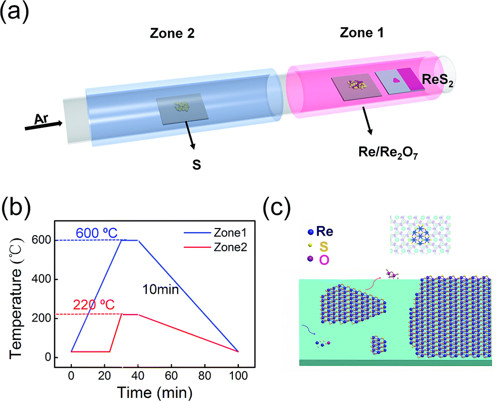 | ||
| Fig. 1 (a) Schematic of the experiment set-up for CVD growth of monolayer ReS2 films. (b) Heating curves of the two zones. (c) Schematic for the epitaxial growth process of ReS2 on mica. Partially reduced Re2O7−x could absorb on the mica surface and act as nucleation sites. | ||
Materials characterization
The morphology of ReS2 films was checked by optical microscope (Zeiss Imager A2m) and atomic force microscope (Bruker Dimension ICON-PT). Raman spectrum was recorded using a LabRAM Raman microscopy system with a 532 nm laser excitation. Si peak at 520 cm−1 was calibrated as a reference for wave number calibration. The point size of laser is 1 μm with a power of 0.5 W to avoid possible thermal effect introduced damage. The elemental compositions and chemical states of ReS2 were investigated by XPS (Phi Quantera). PMMA wet transfer method was taken to transfer ReS2 thin films onto a copper grid for TEM characterization.Device fabrication and electric measurement
Field effect transistors based on ReS2 films were fabricated by evaporating Cr/Au (10/100 nm) electrodes on the top of ReS2 layer using shadow mask method. Before test, the devices were annealed at 300 °C for 4 h in Ar gas to improve the electrical contact. The electrical and optoelectronic properties were measured using semiconductor analyzer (Keithley 4200) on a Lakeshore probe station. A 500 W xenon lamp was used as the light source, and monochromatic lights of 254–850 nm were obtained using optical filters. The intensities of the incident light source were corrected using a power energy meter (Model 372, Scienteck).Result and discussion
Fig. 2a shows the digital photograph of monolayer ReS2 films growth on mica. ReS2 membrane on mica substrate exhibit grey contrast. The optical microscopy of as-grown ReS2 films is given in Fig. 2b, where the monolayer ReS2 films exhibit a slight colour contrast with mica substrate. After transferred onto Si/SiO2 substrate, ReS2 films could still maintain continuous and intact morphology (Fig. S1, ESI†). Atomic force microscopy (AFM) was employed to determine the surface morphology and thickness. As shown in Fig. 2c, the thickness of ReS2 films is about 0.8 nm, corresponding to monolayer structure. With growth time increased to 30 min, the films became thicker with average thickness up to 4.2 nm (Fig. S2, ESI†). It is noteworthy that the surface roughness of monolayer films is very small (Rq = 0.10 nm), while the roughness of multilayer films is much large (Rq = 0.54 nm).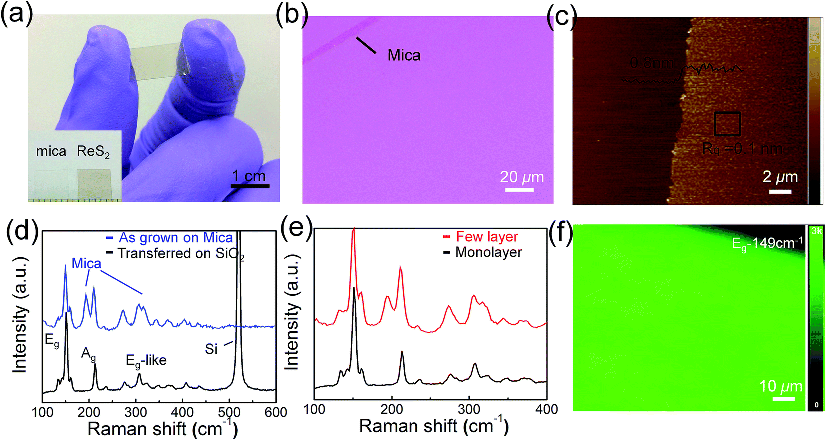 | ||
| Fig. 2 (a) Digital photograph of as-grown ReS2 films on mica substrate. Inset is digital picture of mica substrate with and without ReS2 films. (b) Optical image and (c) AFM tomography image of ReS2 monolayer films. Inset is the height profile. (d) Raman spectra of as-grown ReS2 films on mica and SiO2 substrate. (e) Comparison of Raman spectra between monolayer and multilayer ReS2 films on mica substrate. (f) Raman mapping of monolayer ReS2 films at Eg peak 149 cm−1. | ||
In the Raman spectra of monolayer ReS2 films, two dominant peaks located at 149.1 and 210.4 cm−1 are clearly observed (Fig. 2d), which are assigned to the in-plane (Eg) and out-of-plane (Ag) vibration modes, respectively.29 Several other Raman modes ranging from 100–400 cm−1 may arise from the symmetry splitting introduced by the distorted 1T phase of ReS2.15 Compared to as-synthesized monolayer films on mica, Eg and Ag mode of transferred samples present a slight blueshift by 2.86 and 2.19 cm−1. This could be attributed to the release of tensile strain which arises from the lattice mismatch between ReS2 and mica. Raman mode shift is considered as an effective approach to evaluate the strain in TMDs.31,32 For example, the E2g and A1g peaks of monolayer MoS2 grown on mica both are blueshifted about 3–4 cm−1 due to compressive strain.30 In this work, red shift of Raman modes in ReS2 films indicates the existence of tensile strain. With the increase of film thickness, tensile strain would accumulate and it has to be released by splitting ReS2 films, resulting in lots of cover-like projections as shown in Fig. S3.† Consistent with previous studies,12,15 Raman peaks of multilayer films do not show any difference compared to monolayer samples due to the weak interlayer coupling effect (Fig. 2e). Raman mapping of monolayer ReS2 films was also performed at Eg mode position, and a homogeneous feature in large area up to 100 μm2 scale is presented.
Compared with previous work,23–25 where only isolated ReS2 domains appeared on substrate, the products obtained in our experiment are continuous films. Re2O7 is used as catalyst, which has the lowest melting point (220 °C) among all the rhenium oxide. During the growth process, Re2O7 would rapidly volatilize into vapour phase, and then be reduced by sulfur vapour into Re2O7−x species.23 Subsequently, they are conveyed downstream by Ar gas and absorbed on mica surface, acting as active nucleation sites for further ReS2 growth.
The morphology of ReS2 is very sensitive to the growth time, as shown in Fig. 3. At the beginning, intermediate Re2O7−x species absorbed on mica surface could act as nucleation sites. As temperature go up, Re2O7−x species are further sulfurized into ReS2 with incoming sulfur vapour. Due to low atoms migration energy of mica surface, ReS2 could easily grow along the in-plane direction into monolayer domains. These isolated monolayer ReS2 domains have a small size ranging from 500 nm to 2 μm (Fig. 3a). It is worthy noted that these isolated domains exhibit irregular dendrite shapes, which is very different from traditional TMDs, such as MoS2 and WS2.22,30 This kind of anisotropic growth is attributed to the anisotropic interfacial energy introduced by distorted 1T crystal structure in ReS2. Volatile Re2O7 would easily be run out before reaching 600 °C, and it cannot act as a stable reaction source for growing thick ReS2 films. The main function of Re2O7 is supplying enough nucleation sites for further ReS2 films growth. When the temperature rises up to 600 °C, Re powder start to volatilize and react directly with sulfur into ReS2, which plays the decisive part in multilayer continuous films growth. Isolated ReS2 domains start to interconnect with each other into continuous films as reaction undergoing (Fig. 3b). Typically, when two separate ReS2 domains gather, the edges tend to interconnect rather than overlap, which is the typical characteristic of 2D materials growth.30 After the growth of continuous monolayer films is completed, following ReS2 layers start to emerge on the surface of the first layer (Fig. 3c). We believe that these ReS2 layers should be originated from the zero dimensional or quasi-one-dimensional structures as indicated with white circles in Fig. 3c, suggesting that the ReS2 growth obeys Stranski–Krastanov growth mode.33 In other word, except the first layer, the next layers follow the island-based growth mode, which would result in multilayer films with relatively rough surface. By prolonging the growth time to 30 min, we could obtain multilayer films with thickness about 4.2 nm (Fig. 3d). The surface roughness difference between monolayer and multilayer films further confirms our suggestion (Rq are 0.10 and 0.54 nm, respectively). XRD pattern of multilayer films shows a strong (001) orientation due to the layer-by-layer growth mode on mica substrate (Fig. S4, ESI†).
 | ||
| Fig. 3 (a–d) Schematic (upper) and corresponding AFM topography images (lower row) showing the possible growth mechanism of ReS2: (a) 5 min. (b) 10 min. (c) 15 min. (d) 30 min. Scale bar: 1 μm. (e, f) Schematic growth model for different stages of ReS2 films on mica substrate. | ||
The substrate plays a crucial role in the growth process. As shown in Fig. 3e, atomically smooth and inert chemically surface of mica could facilitate the atoms migration along the surface due to the low energy barrier,34,35 which make the first layer growth on mica surface-dominated and result in continuous monolayer structure. Compared with the very flat epitaxial growth of the first layer on mica, following layers always have relatively rough surface. Because the surface of ReS2 could not provide such low energy for atoms migration as mica, thus the in-plane growth is hindered (Fig. 3f). Compared with other TMDs, such as MoS2 and WS2, and weak van der Waals interaction between layers of the ReS2 could also facilitate the 3D structure growth,36 and accelerate the atoms migration along vertical direction, leading to the rough surface. As shown in Fig. S5,† the products grown on SiO2 substrate exhibit flower-like structures. This is because the rough surface of SiO2 with dangling bonds could increase the energy barrier for atoms migration and prohibit ReS2 from growing along in-plane directions.
Re could directly react with S vapour to form ReS2 under temperature range of 600–900 °C.37 However, the high melting temperature of Re (about 3150 °C) leads to a very low nucleation rate during the growth process. In our experiments, no products appear without Re2O7 under the identical growth conditions. We believe the severe volatilization of Re2O7, which provide adequate nucleation sites for the later ReS2 growth, plays crucial part in monolayer film forming. The dosage of Re2O7 is also important for the growth process. In this experiment, Re2O7 is only one-tenth of the Re power. Only Re2O7 as precursor would result in numerous nanoparticles without ReS2 on mica surface. XPS spectrum shows these particles are mainly composed of Re2O7−x intermediate species (Fig. S6, ESI†). Meanwhile, more Re2O7 could lead to thick film consist with lots of tiny grains with large surface roughness (Fig. S7, ESI†).
X-ray photoelectron spectroscopy (XPS) was performed to determine the stoichiometry of ReS2 films. Fig. 4a shows the survey spectrum of the monolayer ReS2 films. The core 2p3/2 and 2p1/2 level peaks for sulfur are located at 161.37 and 162.63 eV (Fig. 4b). The two dominant level peaks for rhenium are located at 42.6 and 45.1 eV (assigned to Re 4f7/2 and Re 4f5/2 respectively), consistent with previous study36 (Fig. 4c). The prominent 4f7/2 and 4f5/2 peak for Re2O7,38 located at 40.1 and 42.3 eV, are not observed, suggesting the Re2O7 has been completely sulfurized.
 | ||
| Fig. 4 XPS spectra of monolayer ReS2 films. (a) XPS survey spectrum of the sample. Three kinds of elements are present: Re and S (from the sample), Si (from the substrate). (b) XPS spectrum of S 2p and (c) XPS spectrum of Re 4f. | ||
Transmission electron microscope (TEM) analysis was also conducted to explore the crystal structure of ReS2 films. Using a traditional poly(methyl methacrylate) (PMMA) wet transfer method, ReS2 films were transferred onto carbon-supported copper grids. From the low-magnification TEM image, a continuous membrane with obvious folding could be clearly observed (Fig. 5a). Edge folding often appears in TEM analysis of two-dimensional materials, like MoS2 and graphene,30,39 which is probably introduced by the transfer process. HRTEM reveals perfect single-crystal structure of the monolayer films, and clear DS-chains of Re atoms could be seen (Fig. 5b). The angle between a[100] and b[010] is about 60°, which is agree well with the date published on exfoliated ReS2 samples.15 Typical (100) and (010) crystal plane spacing are 0.31 and 0.35 nm, respectively, confirming the high crystallinity of monolayer films. As for the multilayer films, it is demonstrated to be polycrystal consist of many tiny grains with random orientations (Fig. 5c). Fig. 5d shows the HRTEM and corresponding SAED pattern. AED pattern shows clear dim diffraction rings, which further prove the films are polycrystal.
 | ||
| Fig. 5 (a and b) Bright-field TEM and HRTEM images of monolayer ReS2 films. (c and d) Bright-field TEM and HRTEM (STEM) images of few-layer ReS2 films. Insets in (b and d) show corresponding SAED patterns. | ||
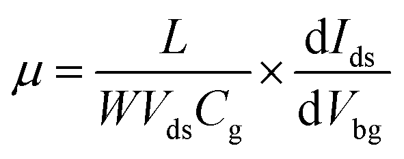
Field effect transistors (FETs) are fabricated based on multilayer ReS2 films (Fig. 6a). It should be noted that previous reports only focus on single crystal ReS2,11,15,24 whereas the performance of multilayer polycrystalline films are still unexplored. The gate-dependent transport curves show a typical n-type behaviour with maximum ON/OFF ratio about 4 × 10³, and the threshold voltage is about −27 V with Vds of 3 V. The carrier mobility could be calculated using following equation:4
 | ||
| Fig. 6 Electrical properties of multilayer ReS2 films. (a) Optical image shows the as-fabricated FET device. (b, c) Output and transfer curve of this device. Back-gate voltage (Vg) sweeping: −30 to 30 V; source-drain bias (Vds): 1 V to 3 V. | ||
The optoelectronic properties of multilayer ReS2 films were also evaluated based on the same FET device. Fig. 7a shows the schematic image of the device, a 500 W xenon lamp was used as the light source with illumination power ranging from 0.25–0.56 mW cm−2. Fig. 7b shows the I–V curves under different incident light intensities. Obviously, the channel current increases significantly under illumination compared to dark condition. Fig. 7c and d shows the photocurrent and responsitivity as a function of light power. Here, photocurrent (ΔI) is the difference between Ion and Ioff with a Vds of 1 V, and the responsitivity is defined as R = ΔI/P × S (P is the light power intensity, and S is the illuminated area of the devices). Both ΔI and R raise slightly with the increase of intensity. The responsivity is estimated to be 0.98 A W−1 at an irradiation intensity of 0.56 mW cm−2, almost one order smaller than that in single-crystal monolayer ReS2 based devices (Fig. S9, ESI†). Time-resolved photoresponse behaviour was probed by switching the light on and off with a time interval of 100 s under a bias of 1 V. The device exhibits a stable and repeatable response to the illumination after 5 cycles (Fig. 7e). A considerable enhancement of current (19 nA) is measured when the device is illuminated by 490 nm light. The response and recovery time is calculated by considering the time it takes to reach 80% of the final values, which are 17.8 and 14.3 s, respectively. Both of the rising time and recovery time of ReS2 films devices are larger than that of exfoliated ReS2 nanosheet,13,40 but comparable to the bilayer polycrystalline film.41 Generally, the active sites of the material significantly affect the rise and decay times.27,42 Based on our measurement condition, gas molecules in air such as oxygen can easily absorbed on the surface of films. Under light illumination, photogenerated carriers would first fill the trap states, which prolongs the response time. We believe the improvement of measurement condition would be effective to improve the responsive speed.43
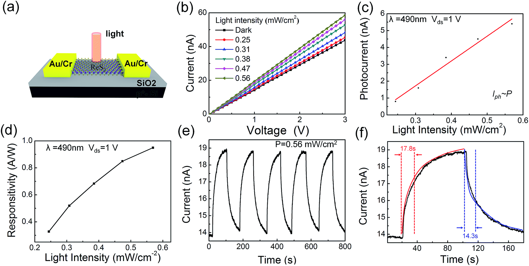 | ||
| Fig. 7 Optoelectronic performance of the phototransistor based on multilayer ReS2 films on SiO2 substrate. (a) Schematic image of the device. (b) I–V curves of device in dark and under 490 nm illumination with different intensities. (c, d) Photocurrent and photoresponsitivity as a function of incident power. (e, f) Time-dependent photoresponse of the device under 490 nm illumination with intensity of 0.56 mW cm−2 and bias of 1 V. | ||
Conclusions
In conclusion, we develop a facile method to obtain large-area continuous ReS2 films on mica substrate using CVD method. Re2O7 acting as catalyst could provide enough seeds for continuous films growth. The multilayer films exhibits a layer-by-layer growth mode with strong (001) orientation. FET measurement indicates that multilayer ReS2 films exhibit n-type transport behaviour with ON/OFF ratio about 4 × 10³ and carrier mobility of 0.27 cm2 V−1 s−1. The optoelectronic properties of ReS2 films are also investigated, with the highest photoresponsivity of 0.98 A W−1 at an illumination intensity of 0.56 mW cm−2. Our work suggests that these scalable ReS2 films may be an ideal candidates for future high performance electronic and optoelectronic devices.Acknowledgements
This work was financially supported by National Natural Science Foundation of China (No. 51572057) and Shandong Provincial Key Lab of Special Welding Technology, Harbin Institute of Technology at Weihai. The authors thanks Prof. Ping-An Hu for assistance on electrical measurements.Notes and references
- N. R. Pradhan, D. Rhodes, S. Feng and Y. Xin, ACS Nano, 2014, 8, 5911–5920 CrossRef CAS PubMed.
- H. Fang, S. Chuang, T. C. Chang, K. Takei, T. Takahashi and A. Javey, Nano Lett., 2012, 12, 3788–3792 CrossRef CAS PubMed.
- Z. Yin, H. Li, H. Li, L. Jiang, Y. Shi and Y. Sun, ACS Nano, 2012, 6, 74–80 CrossRef CAS PubMed.
- B. Radisavljevic, A. Radenovic, J. Brivio, V. Giacometti and A. Kis, Nat. Nanotechnol., 2011, 6, 147–150 CrossRef CAS PubMed.
- Y. Huang, et al., ACS Nano, 2014, 8, 10743–10755 CrossRef CAS PubMed.
- Y. H. Huang, C. C. Peng, R. S. Chen, Y. S. Huang and C. H. Ho, Appl. Phys. Lett., 2014, 105, 093106 CrossRef.
- O. Lopez-Sanchez, D. Lembke, M. Kayci, A. Radenovic and A. Kis, Nat. Nanotechnol., 2013, 8, 497–501 CrossRef CAS PubMed.
- I. G. Lezama, A. Arora, A. Ubaldini, C. Barreteau, E. Giannini, M. Potemski and A. F. Morpurgo, Nano Lett., 2015, 15, 2336–2342 CrossRef CAS PubMed.
- Y. Li, et al., Adv. Funct. Mater., 2016, 26, 293–302 CrossRef CAS.
- Y. Li, C.-Y. Xu and L. Zhen, Appl. Phys. Lett., 2013, 102, 143110 CrossRef.
- Y.-C. Lin, H.-P. Komsa, C.-H. Yeh, T. Björkman, Z.-Y. Liang, C.-H. Ho, Y.-S. Huang, P.-W. Chiu, A. V. Krasheninnikov and K. Suenaga, ACS Nano, 2015, 9, 11249–11257 CrossRef CAS PubMed.
- S. Tongay, et al., Nat. Commun., 2014, 5, 3252 Search PubMed.
- F. Liu, et al., Adv. Funct. Mater., 2016, 26, 1169–1177 CrossRef CAS.
- Q. Zhang, et al., Adv. Mater., 2016, 28, 2616–2623 CrossRef CAS PubMed.
- D. A. Chenet, O. B. Aslan, P. Y. Huang, C. Fan, A. M. van der Zande, T. F. Heinz and J. C. Hone, Nano Lett., 2015, 15, 5667–5672 CrossRef CAS PubMed.
- O. B. Aslan and D. A. Chenet, ACS Photonics, 2016, 3, 96–101 CrossRef CAS.
- N. R. Pradhan, et al., Nano Lett., 2015, 15, 8377–8384 CrossRef CAS PubMed.
- Y. Li, C.-Y. Xu, P. Hu and L. Zhen, ACS Nano, 2013, 7, 7795–7804 CrossRef CAS PubMed.
- Y. Li, C.-Y. Xu, B.-Y. Zhang and L. Zhen, Appl. Phys. Lett., 2013, 103, 033122 CrossRef.
- Y. Zhang, et al., ACS Nano, 2013, 7, 8963–8971 CrossRef CAS PubMed.
- A. L. Elías, et al., ACS Nano, 2013, 7, 5235–5242 CrossRef PubMed.
- W. Zhang, M.-H. Chiu, C.-H. Chen and W. Chen, ACS Nano, 2014, 8, 8653–8661 CrossRef CAS PubMed.
- K. Keyshar, et al., Adv. Mater., 2015, 27, 4640–4648 CrossRef CAS PubMed.
- X. He, F. Liu, P. Hu, W. Fu, X. Wang, Q. Zeng, W. Zhao and Z. Liu, Small, 2015, 11, 5423–5429 CrossRef CAS PubMed.
- F. Cui, et al., Adv. Mater., 2016, 28, 5019–5024 CrossRef CAS PubMed.
- Y. Zhou, Y. Nie, Y. Liu, K. Yan, J. Hong, C. Jin, Y. Zhou, J. Yin, Z. Liu and H. Peng, ACS Nano, 2014, 8, 1485–1490 CrossRef CAS PubMed.
- Q. Wang, M. Safdar, K. Xu, M. Mirza, Z. Wang and J. He, ACS Nano, 2014, 8, 7497–7505 CrossRef CAS PubMed.
- I. R. Beattie, T. R. Gilson and P. J. Jones, Inorg. Chem., 1996, 35, 1301–1304 CrossRef CAS PubMed.
- X.-F. Qiao, J.-B. Wu, L. Zhou, J. Qiao and W. Shi, Nanoscale, 2016, 8, 8324–8332 RSC.
- Q. Ji, et al., Nano Lett., 2013, 13, 3870–3877 CrossRef CAS PubMed.
- Z. H. Ni, T. Yu, Y. H. Lu, Y. Y. Wang, Y. P. Feng and Z. X. Shen, ACS Nano, 2008, 2, 2301–2305 CrossRef CAS PubMed.
- M. Huang, H. Yan, T. F. Heinz and J. Hone, Nano Lett., 2010, 10, 4074–4079 CrossRef CAS PubMed.
- E. Bauer and J. H. van der Merwe, Phys. Rev. B: Condens. Matter Mater. Phys., 1986, 33, 3657 CrossRef CAS.
- Q. Wang, K. Xu, Z. Wang, F. Wang, Y. Huang, M. Safdar, X. Zhan, F. Wang, Z. Cheng and J. He, Nano Lett., 2015, 15, 1183–1189 CrossRef CAS PubMed.
- X. Li, F. Cui, Q. Feng, G. Wang, X. Xu, J. Wu, N. Mao, X. Liang, Z. Zhang and J. Zhang, Nanoscale, 2016, 8, 18956–18962 RSC.
- J. Gao, L. Li, J. Tan, H. Sun, B. Li, J. C. Idrobo, C. V. Singh, T.-M. Lu and N. Koratkar, Nano Lett., 2016, 16, 3780–3787 CrossRef CAS PubMed.
- C.-H. Ho, Opt. Express, 2005, 13, 8–19 CrossRef CAS PubMed.
- Y. Jia, L. Duan, D. Zhang, J. Qiao and G. Dong, J. Phys. Chem. C, 2013, 117, 13763–13769 CAS.
- J. C. Meyer, A. K. Geim, M. I. Katsnelson, K. S. Novoselov, T. J. Booth and S. Roth, Nature, 2007, 446, 60–63 CrossRef CAS PubMed.
- E. Liu, et al., Adv. Funct. Mater., 2016, 26, 1938–1944 CrossRef CAS.
- M. Hafeez, L. Gan, H. Li, Y. Ma and T. Zhai, Adv. Funct. Mater., 2016, 26, 4551–4560 CrossRef CAS.
- Y. Jiang, W. J. Zhang, J. S. Jie, X. M. Meng, X. Fan and S. T. Lee, Adv. Funct. Mater., 2007, 17, 1795–1800 CrossRef CAS.
- J. Zhou, Y. Gu, Y. Hu, W. Mai, P.-H. Yeh, G. Bao, A. K. Sood, D. L. Polla and Z. L. Wang, Appl. Phys. Lett., 2009, 94, 191103 CrossRef PubMed.
Footnote |
| † Electronic supplementary information (ESI) available. See DOI: 10.1039/c7ra01748k |
| This journal is © The Royal Society of Chemistry 2017 |