DOI:
10.1039/C7RA01496A
(Paper)
RSC Adv., 2017,
7, 20206-20211
Temperature-dependence studies of organolead halide perovskite-based metal/semiconductor/metal photodetectors†
Received
6th February 2017
, Accepted 3rd April 2017
First published on 7th April 2017
Abstract
In this paper, polycrystalline perovskite (CH3NH3PbIxCl3−x) photodetectors with a structure of Au/CH3NH3PbIxCl3−x/Au are prepared and are shown to have good performance. The measured electrical parameters demonstrate that the current behavior of the perovskite photodetectors is dependent of work temperature from 300 K to 350 K. We find that only space charge limited conduction mechanism fits the current–voltage (I–V) curves under small external voltage (0.1–0.7 V) both under darkness and illumination. The lattice vibration scattering plays the major role in the dark, leading to a decreased current as the temperature increases under the same external voltage, and an enlarged current increasing with the temperature is due to the leading role of the ionized impurity scattering. At each temperature, the rising slope of the I–V curves decrease with the increase of voltage both under dark and illumination. The values of on/off ratio, responsivity and detectivity increase with the measured temperature, which indicates that the polycrystalline perovskite photodetector can work with better performance at high temperature. However, the stability in the dark gradually becomes weak as the temperature increases, especially at 330 K and above.
1. Introduction
Recently, hybrid organic–inorganic lead halide perovskites (CH3NH3PbX3, where X = Cl, Br, and I) have attracted great attention as light absorbers not only for frequently studied solar cells1–10 but also for (LEDs),11–13 field-effect transistors (FETs),14–16 lasers,17–19 and photodetectors.20–30 The perovskites have excellent semiconductor properties, such as a direct band gap, a broad absorption range and high carrier mobility.23,24 Until now, there are several research works reported on Metal–Semiconductor–Metal (MSM) photodetectors based on Si or GaAs,31–34 and several significant efforts to fabricate high performance CH3NH3PbX3 photodetectors have been made: Makhsud I. et al. produced a light detector showing high gain-bandwidth product using large perovskite single crystals,20 Hao Lu et al. made the first all perovskite self-powered nanosystem by integrating a solar perovskite with a perovskite photodetector,23 and Z. Lian et al. reported a lowest detectable irradiance power density of 2.12 nW cm−2, with the highest responsivity of 953 A W−1 and external quantum efficiency of 2.22 × 10⁵%.24 These high property perovskite photodetectors are prepared with several structures, like Au/perovskites/Au,24,28 Pt/Ti/perovskites/Pt/Ti,26 ITO/perovskites/ITO,27 and the solar cell structures.25,29 Basic electrical parameters such as on/off ratio, responsivity and detectivity are measured under different illumination intensities23,24,27 and optical wavelength.26,27 Although so many remarkable efforts have been made to detect the characteristics of photodetectors based on CH3NH3PbX3 single crystals under different structures and conditions, polycrystalline perovskites photodetectors are rarely discussed, which should be considered owing to their low preparation cost. In addition, temperature-dependence studies are significant for the performance and reliability of the photodetectors, which should be focused on by researchers.
In this work, several Au/CH3NH3PbIxCl3−x/Au photodetectors are prepared and measured. X-ray diffraction (XRD), photoluminescence spectroscopy (PL), and Scanning Electron Microscope (SEM) are given to detect the quality of the perovskite film. Key parameters like on/off ratio, responsivity, detectivity, rise time and fall time are calculated. For detail analysis of the temperature-dependence studies, the electrical parameters are measured under different temperatures vary from 300 K to 350 K (perovskites are considered to decompose at higher temperature). Several current mechanisms are fitted to explain the strange phenomenon of I–V curves.
2. Experimental
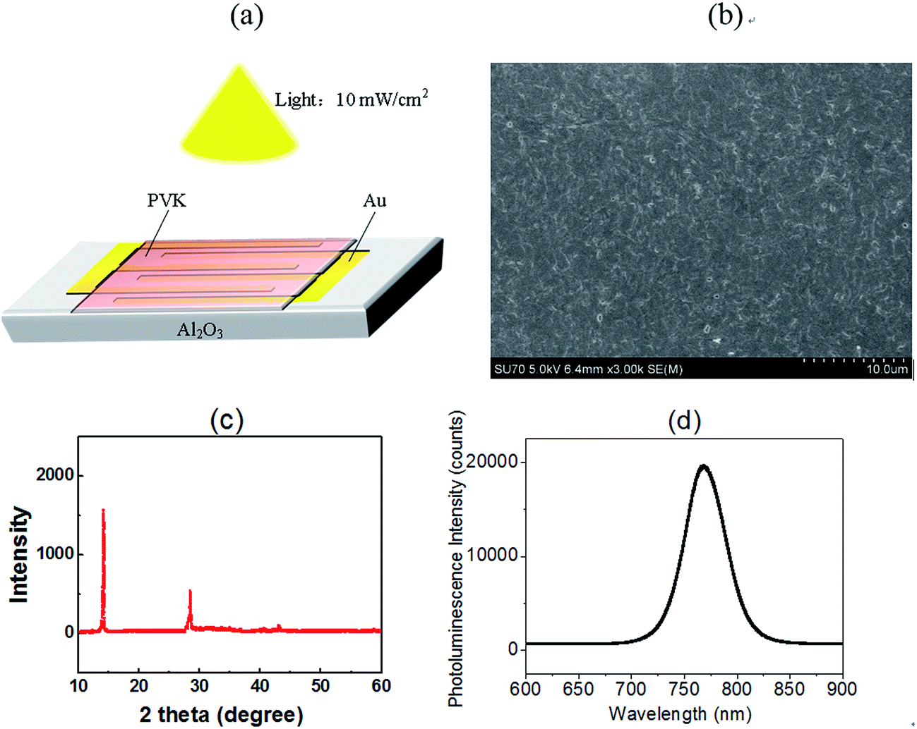
400 μm Al2O3 was employed as the insulating substrate, and a pair of interdigitated Au-film electrodes (2000 μm long and 250 μm wide for each one) were deposited on the substrate, which have 34 fingers and the same interspacing distance of 150 μm. Methylammonium iodide (CH3NH3I) and lead chloride (PbCl2) were prepared according to previous work.26 The preheated precursor solution at 70 °C was used for fabricating the MAPbI3−xClx thin film. Next, the CH3NH3PbI3−xClx precursor solution was spin coated onto the treated substrate at a rate of 4000 rpm for 30 s. The wet perovskite film was then annealed on a hot plate to complete the crystallization. The photodetector with a structure of Au/CH3NH3PbI3−xClx/Au/Al2O3 was completed and shown in Fig. 1(a).
 |
| | Fig. 1 (a) Photodetector with a structure of Au/CH3NH3PbI3−xClx/Au, (b) FE-SEM images of crystallized CH3NH3PbI3−xClx film, (c) XRD data from crystallized CH3NH3PbI3−xClx film, (d) photoluminescence spectroscopy (PL) spectrum of CH3NH3PbI3−xClx film. | |
The diffraction patterns of the CH3NH3PbI3−xClx films were detected by XRD measurements (New D8-Advance, Cu Kα). The steady-state PL measurements were acquired using a fluorescence spectrometer (Horiba FluoroMax®-4) with an excitation wavelength of 460 nm. The surfaces of the PVK films were prepared by SEM (JEOL JSM-6701F). Current–voltage (I–V) measurements were analyzed under different temperatures (300 K, 310 K, 320 K, 330 K, 340 K, and 350 K) and different illumination intensity (dark and 10 mW cm−2) with λ = 550 nm (Keysight B1500A semiconductor parameter analyzer). A solar simulator (xenon lamp, Oriel, AM 1.5G light) and optical attenuators were used for adjustable illumination. The transient photocurrent response was performed under a 550 nm pulse light from a light-emitting diode.
3. Results and discussion
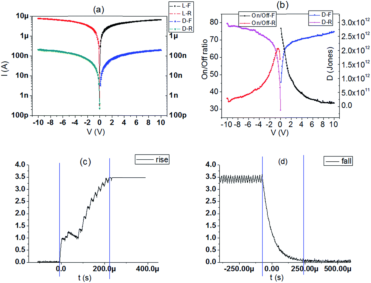
The smooth perovskite film was illustrated by SEM in Fig. 1(b), proving that the polycrystalline PVK film is ideal for device application. Fig. 1(c) gives the XRD measurements of the crystallized perovskite thin film, which strong peaks at 14.08°, 28.41°, and 43.19° can be assigned to (110), (220), and (330) diffractions of CH3NH3PbI3, respectively. PL data of PVK film in Fig. 1(d) indicated a strong bandgap photoluminescence centered at 770 nm. Fig. 2(a) gives the typical current–voltage (I–V) curves of the perovskite photodetector in the dark and under 10 mW cm−2 illumination intensity, the voltage was swept in the sequence 0 → 10 V → 0 V (forward) and 0 → −10 V → 0 V (reverse). Several key parameters are calculated by eqn (1) and (2). On/off ratio is the ratio of photocurrent (Iph) to dark current (Id), responsivity (R) indicates how efficiently the detector responds to an optical signal, and Llight is the incident light power, which is the product of illumination intensity and illumination area (9.9 × 10⁻⁶ m2). For the detectivity (D), q is the elementary charge, and Id is the dark current density when the dark current is dominated by the shot noise.26 The device performance plotted against external bias are illustrated in Fig. 2(b), R is not given in the figure (about 10−2 A W−1) as R is proportional to the current under the same light power. The highest detectivity (3 × 10¹² jones) and highest on/off ratio (77) are shown in Fig. 2(b), indicating a good performance photodetector.| |
 | (1) |
| |
 | (2) |
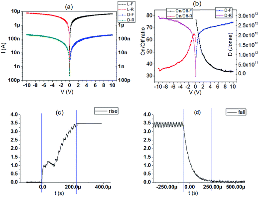 |
| | Fig. 2 (a) Current–voltage (I–V) curves of the perovskite photodetector in the dark and under 10 mW cm−2 illumination intensity, L: light D: dark F: forward R: reverse (b) on/off ratio and detectivity (D) plotted against external bias. (c) Rise time and (d) fall time of photocurrent during switching of light illumination. | |
Fig. 2(a) and (b) illustrates the changed current of the photodetector under dark and light illumination. The on/off ratio is increased with the reduced applied voltage. Herein, the rise time and fall time of the photodetector are defined as the time taken for the 10% to increase to 90% of the peak value. The rise time (180 μs) and fall time (150 μs) are calculated by Fig. 2(c) and (d). The fast response of the device is promising for large-area photodetector applications. Temperature-dependence is a quite significant property for device application. I–V curves of the perovskite photodetector under temperatures vary from 300 K to 350 K are illustrated in Fig. 3(a) and (b). Strange phenomenon is observed that the photocurrent rises and the dark current falls as the temperature increases. For each temperature, the rising slope of the I–V curve decreases with the increase of voltage.
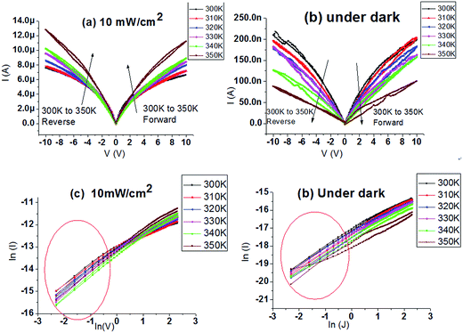 |
| | Fig. 3 I–V curves of the perovskite photodetector as a function of temperature from 300 K to 350 K (a) under illumination of 10 mW cm−2, (b) in the dark. F: forward R: reverse. SCLC mechanism fitting curves at temperatures vary from 300 K to 350 K (c) under illumination of 10 mW cm−2, (d) in the dark. | |
Several current mechanisms are applied to explain the phenomenon: space charge limited conduction (SCLC), Poole Frankel conduction (P–F), Fowler Nordheim tunneling (F–N tunneling).35,36 The definition and fitting formula are given in ESI.† We found only SCLC mechanism fits the I–V curves under small external voltage (0.1–0.7 V) both under dark and illumination as shown in Fig. 3(c) and (d), indicating that the I–V curves fit ohmic characteristics when low voltage is applied. F–N tunneling and P–F mechanisms are not suitable here, seen in Fig. S1.†
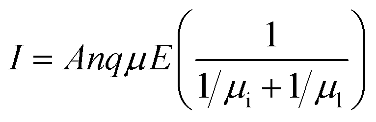
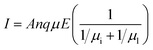
Here we consider the scattering mechanism should be responsible for the phenomenon in Fig. 2. There are two main carrier scattering mechanisms: ionized impurity scattering and lattice vibration scattering. Relationships between current and carrier scattering are shown in eqn (3)–(5).
| |
 | (3) |
where
A is area,
n is the concentration of carriers,
q is carrier charge,
μ is mobility,
E is electrical field,
μi is the mobility governed by ionized impurity scattering,
μl is the mobility governed by lattice vibration scattering,
Ni is concentration of the ionized impurity, and
T is the temperature. The lattice vibration scattering plays the major role in the dark where the concentration of carriers is quite low. The current will decrease as the temperature increases under the same applied voltage without illumination. As photo-induced carriers enlarge
n in
eqn (3), the current increases drastically under illumination compare to that in the dark, and the leading role of scattering mechanism changes to the ionized impurity scattering, which means the current will enlarge with the increase of the temperature under the same external voltage. As for each temperature (in the dark and under light), the rising slope of the
I–
V curve decreases with the increase of voltage. This is because the concentration of carriers will not increase under the same light illumination power, and the product of electrical field and the mobility will gradually approach to the limit. The value of current will reach 15 μA as the product of electrical field and the mobility will gradually approach to the limit (seen in Fig. S2
†), proving the conclusion above. The whole current mechanisms based on different applied voltage are summarized and given in
Fig. 4(a).
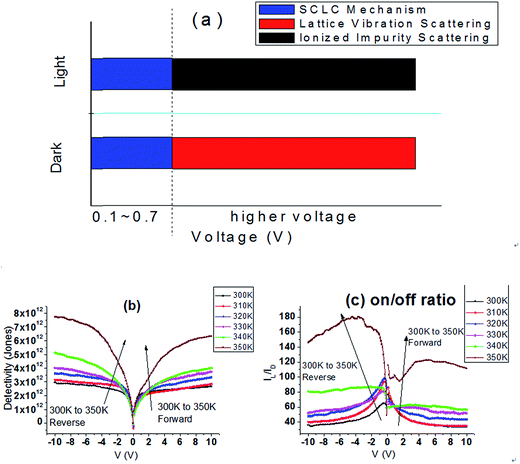 |
| | Fig. 4 (a) Current mechanisms based on different applied voltage, (b) detectivity and (c) on/off ratio plotted against external bias under temperatures vary from 300 K to 350 K, F: forward R: reverse. | |
The organic–inorganic metal halide perovskite is said to be very unstable, especially under high temperature for a long time. Hence, the effect of temperature on the stability and performance of perovskite-based photodetector as a function of operation time (0, 5, 10, and 30 min) is given in Fig. S3(a)–(l).† The photodetector under illumination shows stable properties even after 350 K heat treatment of 30 min. However, the stability in the dark gradually becomes week as the temperature increases. The XRD spectra and UV-Vis spectra of perovskite layer at different temperatures are provided in Fig. S4(a) and (b).† PbI2 is seen due to the partial thermal decomposition of the perovskite when the temperature climbs to 330 K and above, but the absorption curves under each temperature show nearly no changes. Key parameters like on/off ratio and detectivity of the perovskite photodetectors are calculated and illustrated in Fig. 4(b) and (c). Responsivity is proportional to the photocurrent. It is obvious that the on/off ratio, responsivity and detectivity increase as the temperature increase, which indicates that the perovskite photodetector can gain better performance at high temperature (300 K to 350 K). But when considering the stability by operating for 30 min or more, the performance under high temperature (340–350 K) may be reduced by the jumping dark current.
4. Conclusions
In this work, the polycrystalline perovskite film was applied to fabricate photodetectors, suggesting an ideal material for device application. Key parameters like on/off ratio, responsivity, detectivity, rise time and fall time are calculated, proving that the photodetectors are in good performance. For a detail analysis of the temperature-dependence studies, the photodetectors based perovskites demonstrate different current curves at different temperatures. Under small external voltage, SCLC mechanism fits well the dark and illumination I–V curves. The lattice vibration scattering plays the major role in the dark, leading to the decrease of current as the temperature increases. At each temperature, the rising slope of the I–V curve decreases with the increased voltage because the product of electrical field and the mobility will gradually approach to the limit. The effect of temperature on the stability shows that the stability in the dark gradually becomes week as the temperature increases, especially in 330 K and above. The values of on/off ratio, responsivity and detectivity increase with the measured temperature, which indicates that the polycrystalline perovskite photodetector can work with better performance at high temperature. However, the performance under high temperature (340–350 K) may be reduced due to the jumping dark current.
Acknowledgements
The authors would like to acknowledge the financial support from the National Natural Science Foundation, China (Grant No. 51472196 and No. 61234006).
References
- C. Zuo, H. J. Bolink, H. Han, J. Huang, D. Cahen and L. Ding, Advances in Perovskite Solar Cells, Adv. Sci., 2016, 3, 1500324 CrossRef PubMed
 .
. - Z. Zhu, C. C. Chueh, F. Lin and A. K. Jen, Enhanced Ambient Stability of Efficient Perovskite Solar Cells by Employing a Modified Fullerene Cathode Interlayer, Adv. Sci., 2016, 3, 1600027 CrossRef PubMed .
- W. Zhu, C. Bao, F. Li, X. Zhou, J. Yang, T. Yu and Z. Zou, An efficient planar-heterojunction solar cell based on wide-bandgap CH3NH3PbI2.1Br0.9 perovskite film for tandem cell application, Chem. Commun., 2016, 52, 304–307 RSC .
- W. Zhu, C. Bao, F. Li, T. Yu, H. Gao, Y. Yi and Z. Zou, A halide exchange engineering for CH3NH3PbI3−xBrx perovskite solar cells with high performance and stability, Nano Energy, 2016, 19, 17–26 CrossRef CAS .
- Y. Zhou, M. Yang, O. S. Game, W. Wu, J. Kwun, M. A. Strauss and N. P. Padture, Manipulating Crystallization of Organolead Mixed-Halide Thin Films in Antisolvent Baths for Wide-Bandgap Perovskite Solar Cells, ACS Appl. Mater. Interfaces, 2016, 8, 2232–2237 CAS .
- Z. Zhao, X. Chen, H. Wu, X. Wu and G. Cao, Probing the Photovoltage and Photocurrent in Perovskite Solar Cells with Nanoscale Resolution, Adv. Funct. Mater., 2016, 26, 3048–3058 CrossRef CAS .
- Z. Yang, C. C. Chueh, P. W. Liang, M. Crump, F. Lin, Z. Zhu and A. K. Y. Jen, Effects of formamidinium and bromide ion substitution in methylammonium lead triiodide toward high-performance perovskite solar cells, Nano Energy, 2016, 22, 328–337 CrossRef CAS .
- Q. Xue, G. Chen, M. Liu, J. Xiao, Z. Chen, Z. Hu and H. L. Yip, Improving Film Formation and Photovoltage of Highly Efficient Inverted-Type Perovskite Solar Cells through the Incorporation of New Polymeric Hole Selective Layers, Adv. Energy Mater., 2016, 6, 1502021 CrossRef .
- Y. Zhao, J. Wei, H. Li, Y. Yan, W. Zhou, D. Yu and Q. Zhao, A polymer scaffold for self-healing perovskite solar cells, Nat. Commun., 2016, 7, 10228 CrossRef CAS PubMed .
- Y. Shao, Y. Yuan and J. Huang, Correlation of energy disorder and open-circuit voltage in hybrid perovskite solar cells, Nat. Energy, 2016, 1, 15001 CrossRef CAS .
- X. Gong, Z. Yang, G. Walters, R. Comin, Z. Ning, E. Beauregard and E. H. Sargent, Highly efficient quantum dot near-infrared light-emitting diodes, Nat. Photonics, 2016, 10, 253–257 CrossRef CAS .
- H. Cho, S. H. Jeong, M. H. Park, Y. H. Kim, C. Wolf, C. L. Lee and S. H. Im, Overcoming the electroluminescence efficiency limitations of perovskite light-emitting diodes, Science, 2015, 350, 1222–1225 CrossRef CAS PubMed .
- Z. K. Tan, R. S. Moghaddam, M. L. Lai, P. Docampo, R. Higler, F. Deschler and F. Hanusch, Bright light-emitting diodes based on organometal halide perovskite, Nat. Nanotechnol., 2014, 9, 687–692 CrossRef CAS PubMed .
- X. Y. Chin, D. Cortecchia, J. Yin, A. Bruno and C. Soci, Lead iodide perovskite light-emitting field-effect transistor, Nat. Commun., 2015, 6, 7383 CrossRef CAS PubMed .
- F. Li, C. Ma, H. Wang, W. Hu, W. Yu, A. D. Sheikh and T. Wu, Ambipolar solution-processed hybrid perovskite phototransistors, Nat. Commun., 2015, 6, 8238 CrossRef PubMed .
- Y. Wang, Y. Zhang, Y. Lu, W. Xu, H. Mu, C. Chen and Y. B. Cheng, Hybrid Graphene-Perovskite Phototransistors with Ultrahigh Responsivity and Gain, Adv. Opt. Mater., 2015, 3, 1389–1396 CrossRef CAS .
- U. Bansode, R. Naphade, O. Game, S. Agarkar and S. Ogale, Hybrid Perovskite Films by a New Variant of Pulsed Excimer Laser Deposition: A Room-Temperature Dry Process, J. Phys. Chem. C, 2015, 119, 9177–9185 CAS .
- S. Chen, K. Roh, J. Lee, W. K. Chong, Y. Lu, N. Mathews and A. Nurmikko, A Photonic Crystal Laser from Solution Based Organo-Lead Iodide Perovskite Thin Film, ACS Nano, 2016, 10, 3959–3967 CrossRef CAS PubMed .
- Z. Gu, K. Wang, W. Sun, J. Li, S. Liu, Q. Song and S. Xiao, Two-Photon Pumped CH3NH3PbBr3 Perovskite Microwire Lasers, Adv. Opt. Mater., 2016, 4, 472–479 CrossRef CAS .
- M. I. Saidaminov, V. Adinolfi, R. Comin, A. L. Abdelhady, W. Peng, I. Dursun and O. M. Bakr, Planar-integrated single-crystalline perovskite photodetectors, Nat. Commun., 2015, 6, 8724 CrossRef CAS PubMed .
- B. R. Sutherland, A. K. Johnston, A. H. Ip, J. Xu, V. Adinolfi, P. Kanjanaboos and E. H. Sargent, Sensitive, Fast, and Stable Perovskite Photodetectors Exploiting Interface Engineering, ACS Photonics, 2015, 2, 1117–1123 CrossRef CAS .
- H. Wei, Y. Fang, P. Mulligan, W. Chuirazzi, H. H. Fang, C. Wang and J. Huang, Sensitive X-ray detectors made of methylammonium lead tribromide perovskite single crystals, Nat. Photonics, 2016, 10, 333–339 CrossRef CAS .
- H. Lu, W. Tian, F. Cao, Y. Ma, B. Gu and L. Li, A Self-Powered and Stable All-Perovskite Photodetector-Solar Cell Nanosystem, Adv. Funct. Mater., 2016, 26, 1296–1302 CrossRef CAS .
- Z. Lian, Q. Yan, Q. Lv, Y. Wang, L. Liu, L. Zhang and J. L. Sun, High-Performance Planar-Type Photodetector on (100) Facet of MAPbI3 Single Crystal, Sci. Rep., 2015, 5, 16563 CrossRef PubMed .
- D. Li, G. Dong, W. Li and L. Wang, High performance organic–inorganic perovskite-optocoupler based on low-voltage and fast response perovskite compound photodetector, Sci. Rep., 2015, 5, 7902 CrossRef CAS PubMed .
- K. C. Kwon, K. Hong, L. Q. Van, S. Y. Lee, J. Choi, K. B. Kim and H. W. Jang, Inhibition of Ion Migration for Reliable Operation of Organolead Halide Perovskite-Based Metal/Semiconductor/Metal Broadband Photodetectors, Adv. Funct. Mater., 2016, 26, 4213–4222 CrossRef CAS .
- X. Hu, X. Zhang, L. Liang, J. Bao, S. Li, W. Yang and Y. Xie, High-Performance Flexible Broadband Photodetector Based on Organolead Halide Perovskite, Adv. Funct. Mater., 2014, 24, 7373–7380 CrossRef CAS .
- H. Fang, Q. Li, J. Ding, N. Li, H. Tian, L. Zhang and Q. Yan, A self-powered organolead halide perovskite single crystal photodetector driven by a DVD-based triboelectric nanogenerator, J. Mater. Chem. C, 2016, 4, 630–636 RSC .
- L. Dou, Y. M. Yang, J. You, Z. Hong, W. H. Chang, G. Li and Y. Yang, Solution-processed hybrid perovskite photodetectors with high detectivity, Nat. Commun., 2014, 5, 5404 CrossRef CAS PubMed .
- J. Chen, S. Zhou, S. Jin, H. Li and T. Zhai, Crystal organometal halide perovskites with promising optoelectronic applications, J. Mater. Chem. C, 2016, 4, 11–27 RSC .
-
(a) A. Slonopas, B. J. Foley, J. J. Choi and M. C. Gupta, Charge transport in bulk CH3NH3PbI3 perovskite, J. Appl. Phys., 2016, 119, 074101 CrossRef ;
(b) F. F. Masouleh, N. Das and H. R. Mashayekhi, Assessment of amplifying effects of ridges spacing and height on nano-structured MSM photo-detectors, Opt. Quantum Electron., 2014, 47, 193–201 CrossRef .
-
(a) Q. Dong, Y. Fang, Y. Shao, P. Mulligan, J. Qiu, L. Cao and J. Huang, Electron-hole diffusion lengths > 175 μm in solution-grown CH3NH3PbI3 single crystals, Science, 2015, 347, 967 CrossRef CAS PubMed ;
(b) N. Das, M. F. Fadakar and H. R. Mashayekhi, A Comprehensive Analysis of Plasmonics-Based GaAs MSM-Photodetector for High Bandwidth-Product Responsivity, Adv. OptoElectron., 2013, 1–10 CrossRef .
- F. F. Masouleh, N. Das and H. R. Mashayekhi, Optimization of light transmission efficiency for nano-grating assisted MSM-PDs by varying physical parameters, Photonics and Nanostructures, 2014, 12, 45–53 CrossRef .
- F. F. Masouleh, N. Das and S. M. Rozati, Optimal subwavelength design for efficient light trapping in central slit of plasmonics-based metal–semiconductor–metal photodetector, Opt. Quantum Electron., 2015, 47, 1477–1485 CrossRef CAS .
- A. Slonopas, B. J. Foley, J. J. Choi and M. C. Gupta, Charge transport in bulk CH3NH3PbI3 perovskite, J. Appl. Phys., 2016, 119, 074101 CrossRef .
- Q. Dong, Y. Fang, Y. Shao, P. Mulligan, J. Qiu, L. Cao and J. Huang, Electron-hole diffusion lengths > 175 μm in solution-grown CH3NH3PbI3 single crystals, Science, 2015, 347, 967 CrossRef CAS PubMed .
Footnote |
| † Electronic supplementary information (ESI) available: See supplementary material for the current mechanisms of the studied photodetectors. See DOI: 10.1039/c7ra01496a |
|
| This journal is © The Royal Society of Chemistry 2017 |
Click here to see how this site uses Cookies. View our privacy policy here. 
 Open Access Article
 This Open Access Article is licensed under a
  *a
*a