
 Open Access Article
 This Open Access Article is licensed under a Creative Commons Attribution-Non Commercial 3.0 Unported Licence
The morphological effect on electronic structure and electrical transport properties of one-dimensional carbon nanostructures
Jing Gao,
Yujin Ji,
Youyong Li ,
Jun Zhong* and
Xuhui Sun*
,
Jun Zhong* and
Xuhui Sun*
Institute of Functional Nano and Soft Materials Laboratory (FUNSOM), Jiangsu Key Laboratory for Carbon-Based Functional Materials & Devices, Soochow University, Suzhou, Jiangsu 215123, China. E-mail: jzhong@suda.edu.cn; xhsun@suda.edu.cn
First published on 12th April 2017
Abstract
Aligned one-dimensional carbon nanostructures with different morphologies such as carbon nanotubes (CNTs) and carbon nanofibers (CNFs) have been synthesized by the plasma-enhanced chemical vapor deposition method with different catalyst/underlayer combinations. The electronic structures of CNTs and CNFs have been studied by X-ray absorption near-edge structure spectroscopy (XANES), which reveals that CNTs have much fewer oxidized groups than CNFs. Moreover, the electrical transport properties of a single CNT or CNF have been measured in situ under transmission electron microscopy observation and the results show that CNTs have 2 orders lower resistivity than that of CNFs. A single CNT can be applied with higher voltage and larger current before thermal breakdown compared to a single CNF, which can be related to the electronic structure as revealed by XANES. Our results offer a good example of examining the relationship between morphological structure, electronic structure and electrical transport properties in carbon nanomaterials, which will certainly be useful in the applications of nano-devices.
1. Introduction
Carbon-based nanostructures have attracted a lot of interest in recent decades due to their unique properties and various potential applications.1–3 In particular, vertically aligned carbon nanotubes (CNTs) or carbon nanofibers (CNFs) have been considered to be excellent materials for nanoelectrode arrays, nanoelectromechanical devices, or field emission devices.1–5 Different methods have been used to fabricate these materials and the controlled growth for a designed geometry is still under way.4–11 For example, by using a tailored trilayered catalyst, highly uniform and dense arrays of vertically aligned single-walled carbon nanotubes (SWCNTs) were prepared.11 Recently, the growth behaviors of vertically aligned CNTs and CNFs grown on different underlayer metals by plasma-enhanced chemical vapor deposition (PECVD) methods were also investigated.12 The results showed that the choice of catalyst/underlayer combination played an important role for the control of average diameter, diameter distribution, density, growth rate and contact resistance of the products. Although the morphology of various carbon nanostructures has been carefully compared, the electronic structure has not been further studied. The electrical transport properties of CNTs and CNFs related to different morphological structures and electronic structures also need to be clarified which will be particularly useful in nano-devices. For example, CNTs can be used as building blocks in nanoelectronics and their electrical transport property will significantly affect the device performance.1 Carbon nanostructures can also used in gas sensors and the tuning of their electronic structure such as controlled introduction of structural defects has been reported as an effective way to improve the device performance.5 The relationship among morphological structure, electronic structure and electrical transport property in carbon nanomaterials is thus important for their future applications.In this study CNTs and CNFs have been synthesized by PECVD method with different catalyst/underlayer combinations. The electronic structure of CNTs and CNFs has been studied by X-ray absorption near-edge structure spectroscopy (XANES). XANES is an element-specific spectroscopic technique involving the excitation of electrons from a core level to the empty states.13–15 It is an important element-specific characterization tool which is capable of obtaining electronic, structural and bonding information in carbon based systems.13–15 The XANES results reveal that CNTs have much less oxidized groups than CNFs. The electrical transport property measurement shows that 2 orders lower electrical resistivity can be observed in CNTs than that in CNFs and much higher voltage and larger current can be applied on CNTs before the thermal breakdown. Our results offer a good example to examine the relationship of morphological structure, electronic structure and electrical transport property in carbon nanomaterials.
2. Experimental section
The metal underlayer (Ti, Cr or Al) was evaporated directly on Si substrate to the thickness of 10, 30 or 80 nm followed by the evaporation of Fe or Ni thin film (5, 10 or 20 nm) as catalysts using electron-beam evaporation deposition.12 Then the materials were pre-treated by thermal annealing at 600 °C under 2 mbar NH3 atmosphere for 3 min and the catalyst thin films were broken down to the nanoparticles. A direct current PECVD (Black Magic, AIXTRON) was used for the growth of the carbon nanostructures.12 In the growth process, the substrate was firstly heated to a temperature of 750 °C and then the mixed gas of NH3 and C2H2 (4![[thin space (1/6-em)]](https://www.rsc.org/images/entities/char_2009.gif) :1) were introduced into the reaction chamber until a pressure of 7 Torr. The plasma was 210 W with an applied voltage of 530 V. The growth period was 15 min for all samples. After growth, the samples were cooled down to room temperature before exposed to the air.
:1) were introduced into the reaction chamber until a pressure of 7 Torr. The plasma was 210 W with an applied voltage of 530 V. The growth period was 15 min for all samples. After growth, the samples were cooled down to room temperature before exposed to the air.
All samples have been shown to be aligned carbon-based nanostructures on substrates.12 High-resolution transmission electron microscopy (HRTEM) (FEI Tecnai G2 F20 S-TIWN) was used to characterize the morphology of the as-synthesized products. The electrical transport properties of individual carbon nanostructure have been in situ measured using the TEM-STM holder (Nanofactory) under TEM observation. XANES experiments were performed on the SGM beamline at the Canadian Light Source (CLS). All the spectra were recorded at room temperature with a resolution of 0.2 eV at the C K-edge with the total electron yield (TEY) detection mode. The spectra were normalized at the pre-edge position and the post-edge position around 300 eV to clearly show the difference between 283 eV and 295 eV.
3. Results and discussion
3.1 Morphology and electronic structure
Fig. 1 shows TEM images of carbon nanostructures synthesized with Ni catalyst and different metal underlayers: (a) 10 nm Ni/10 nm Al/Ti underlayer (labeled as Ni-CNTs), (b) 20 nm Ni/Cr underlayer (labeled as Ni-CNFs-1), and (c) 20 nm Ni/Ti underlayer (labeled as Ni-CNFs-2). The TEM image for 10 Ni/10 Al/Ti sample in Fig. 1(a) shows a tube-like structure with a hollow center and thin tube walls. It can be assigned to carbon nanotubes synthesized with PECVD. Thus we label it as Ni-CNTs. However, different structures can be observed in Fig. 1(b) and (c) for the other two samples with different underlayers. The TEM images for the two samples show a small hollow center but a thick tube wall. In TEM images the thick wall shows a stacking cone-like structure without clear concentric cylindrical carbon layers as that for multi-walled carbon nanotubes (MWCNTs). The ratio of the wall to the inner hollow structure is very big and we thus attribute this structure to carbon nanofiber (the two samples are labeled as Ni-CNFs-1 and Ni-CNFs-2, respectively). The different structures for Ni-CNTs (10 Ni/10 Al/Ti underlayer) and Ni-CNFs-1 (or Ni-CNFs-2) can be related to the additional Al layer between the top Ni catalysts and the Ti underlayer. The different catalyst sizes may also lead to the different carbon structures. For Ni-CNTs, the catalyst size is smaller (10 nm Ni) leading to the formation of CNTs with a smaller outer diameter around 50 nm. While for Ni-CNFs-1 or Ni-CNFs-1 (the catalyst is 20 nm Ni, larger than that for Ni-CNTs), the catalyst size is larger leading to the formation of CNFs with an outer diameter around 140 nm (the inner diameter is similar to that of CNTs). The larger size of the catalyst particle may lead to the formation of CNFs with larger outer diameter.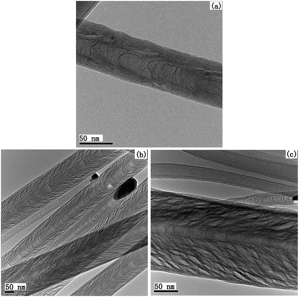 | ||
| Fig. 1 TEM images of various carbon nanostructures: (a) Ni-CNTs (10 nm Ni/10 nm Al/Ti underlayer), (b) Ni-CNFs-1 (20 nm Ni/Cr underlayer), and (c) Ni-CNFs-2 (20 nm Ni/Ti underlayer). | ||
To investigate the electronic structures of the two different structures, C K-edge XANES experiments have been performed and the results are shown in Fig. 2. The XANES spectrum of commercial MWCNTs is also shown for comparison. The spectrum for MWCNTs is characterized by three main features: A, B and C at about 285.5, 288.4 and 292.5 eV, respectively. The spectral shape is in good agreement with the previous reports.13–15 According to the literatures, the feature A is univocally assigned to the π* excitation of C–C bonds in a C ring structure and the feature C to the σ* excitation,13–16 while the feature B to sp3 hybridized states due to various modification groups such as COOH or C–O bonds.13–17 Feature B for MWCNTs is weak, indicating weak modification. However, curve b for Ni-CNTs (10 nm Ni/10 nm Al/Ti underlayer) shows a prominent feature B, indicating increased oxidation groups compared to pure MWCNTs.13–15 Oxidized groups can be expected in the high temperature growth process of CNTs, which could be the origin of increased feature B.13–15 Defects produced in the growth process may also contribute to the formation of feature B. A decreased feature C can also be observed. The feature C stands for a long range order of carbon ring structure according to the ref. 14 The present CNTs prepared by PECVD method have more oxidized groups (a prominent feature B) than MWCNTs, thus the spectrum of Ni-CNTs has less long range order and shows a decreased intensity of feature C.14 A feature at 290.8 eV (labeled as C′ in the revised manuscript) can also be observed, which can be attributed to CO32+ groups produced in the growth process.17 The feature C′ can be found in all the samples (both CNTs and CNFs) with similar intensity.
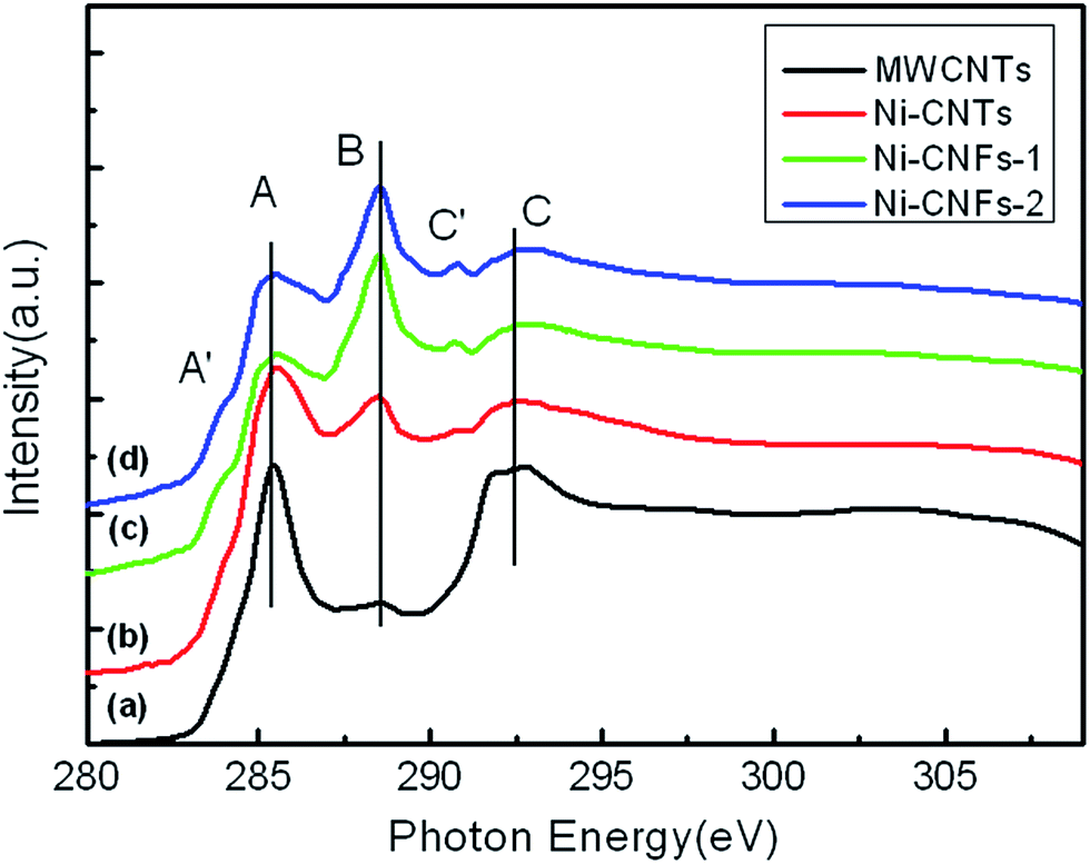 | ||
| Fig. 2 Comparison of the C K-edge XANES spectra of (a) commercial MWCNTs, (b) Ni-CNTs, (c) Ni-CNFs-1, and (d) Ni-CNFs-2. | ||
When observing the XANES spectra of Ni-CNFs-1 and Ni-CNFs-2 in Fig. 2(c) and (d), respectively, even stronger feature B can be found indicating much more oxidized groups compared to Ni-CNTs. Feature B is a dominant feature for the CNF samples (much higher than feature A). The sharply increased intensity of feature B can be attributed to the heavily oxidized nature of the thick CNF wall, which shows a major electronic structure difference when compared to CNTs. The simultaneously decreased feature A for CNFs also confirms the higher oxidization.13–16 The TEM images of CNFs also show irregular stacking cone-like carbon structure of the thick fiber wall. The increased feature B and the decreased feature A clearly show the lose of tube ring structure and the formation of irregular stacking cone-like structure in CNFs, which are the main difference between CNTs and CNFs produced by similar method.
The carbon nanostructures grown with Fe catalysts have also been investigated. Fig. 3 shows the TEM images of carbon nanostructures grown with (a) 5 nm Fe/10 nm Al/Ti underlayer (labeled as Fe-CNTs-1) and (b) 20 nm Fe/Ti underlayer (labeled as Fe-CNTs-2). Both images show a tube-like structure with a hollow center and thin tube walls regardless of the catalyst size or the absence of the additional Al layer, indicating the structural difference between using Ni and Fe as catalysts. Fig. 3(c) shows the high-resolution TEM image of Fe-CNTs-2, which clearly reveals the existence of coherent graphitic layers as the tube wall. For the CNF sample it has a thick wall without coherent graphitic layers. Some stacking cone-like structures in the CNT samples (Fig. 3(a) and (b)) can also be observed similar to that in CNFs. However, they are actually some wrinkle structures on the tube wall. The present CNT has a large inner diameter (around 40 nm) which is much larger than the tube wall thickness, thus it is easy to form wrinkle structures on the tube wall. It can be clearly observed in Fig. 3(c). An internal hollow structure in Fig. 3(c) can also be observed confirming the CNT structure.
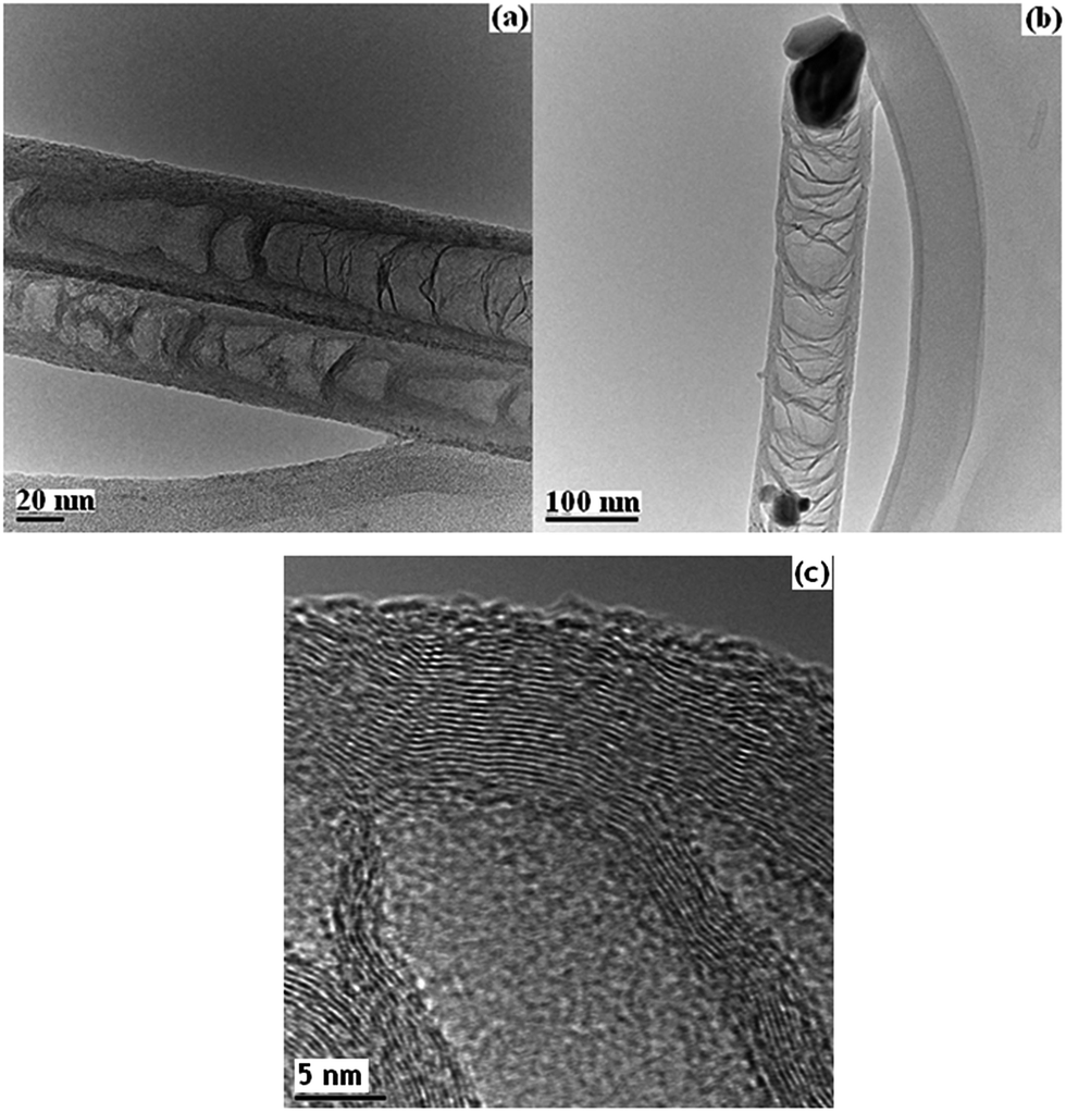 | ||
| Fig. 3 TEM images of different carbon-based nanostructures: (a) Fe-CNTs-1 (5 nm Fe/10 nm Al/Ti underlayer) and (b) Fe-CNTs-2 (20 nm Fe/Ti underlayer). (c) High-resolution TEM image of Fe-CNTs-2 to show the graphitic layers and the winkle structure on the tube wall. | ||
To study the electronic structure of CNTs grown by Fe catalysts, C K-edge XANES spectra of Fe-CNTs-1 and Fe-CNTs-2 are shown in Fig. 4 with a comparison of the spectra of Ni-CNFs-2 and commercial MWCNTs. Clearly, both curves b and c for CNTs grown with Fe catalysts show similar spectral shape as that for Ni-CNTs in Fig. 2, with increased feature B compared to that for MWCNTs standing for more oxidized groups. However, the spectra of CNTs are significantly different from that of CNFs (Ni-CNFs-2) which shows a dominant feature B for heavily oxidized fiber wall, confirming the electronic structure difference between CNTs and CNFs.
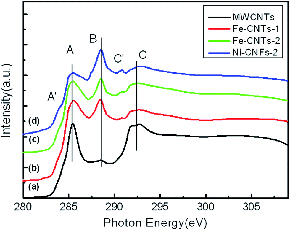 | ||
| Fig. 4 Comparison of the C K-edge XANES spectra of (a) commercial MWCNTs, (b) Fe-CNTs-1, (c) Fe-CNTs-2, and (d) Ni-CNFs-2. | ||
3.2 Electrical transport property
The electrical transport properties of individual CNTs and CNFs are further investigated by means of a “Nanofactory Instruments” piezo-holders inserted into a FEI Tecnai G2 F20 operated at 200 kV field-emission HRTEM. Carbon nanostructures have been considered to be excellent materials in nano-devices and their electrical properties are thus important for potential applications.1,2 We have revealed the electronic structure difference between CNTs and CNFs by the XANES spectra and try to further show their electrical transport difference by the in situ TEM measurements. The individual CNF or CNT samples were mounted onto a fresh-cut Au support wire (0.33 mm in diameter) by dipping into their powders. The CNFs or CNTs were attached to the Au wires due to adhesion forces and then attached to the counter electrode, a sharply etched scanning tunnel microscope (STM) tungsten tip, by means of subtle piezo-movements of the sample wire. The TEM image of a CNF mounted between two electrodes is shown in Fig. 5(a) (Ni-CNFs-1). The inset picture shows the magnified image of the sample with a typical CNF structure. The CNF is tightly attached to the tungsten tip by moving the electrode forward and a slightly bended structure can be observed. Moreover, a focused beam is exposed on the contact point of the fiber and the tungsten tip for 1 min, which may significantly improve the connection. I–V curves of the CNF before and after the beam focusing are shown in Fig. 5(e). Both curves exhibit linear shape suggesting metallic properties. It is clear that after the beam focusing a better connection can be achieved with lower resistance. The measured resistances for the CNF before and after the beam focusing are 1700 kΩ and 1000 kΩ, respectively. The calculated resistivity of the CNF after the beam focusing is about 1.35 × 10⁻² Ω·m. The same treatment is applied to several other CNFs (five CNFs) prepared with Ni catalysts and similar resistivity can be observed.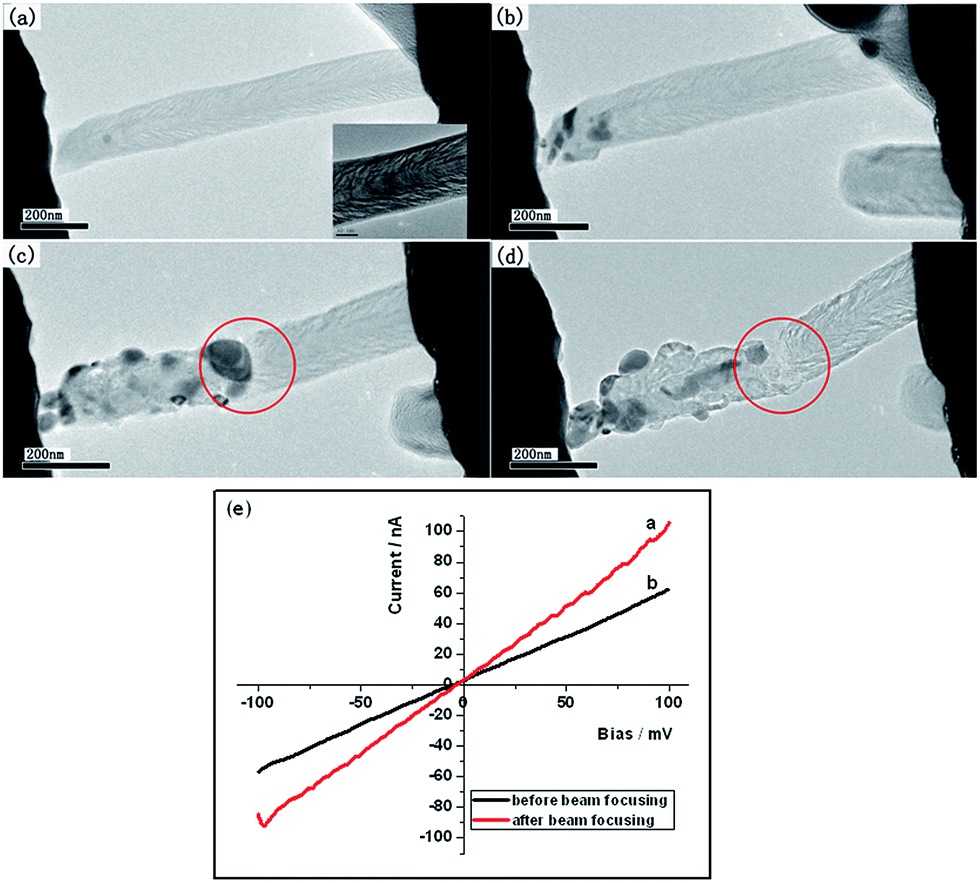 | ||
| Fig. 5 (a–d) TEM images of the thermal breakdown process of Ni-CNFs-1. (e) I–V curves of Ni-CNFs-1 before (black) and after (red) beam focusing. | ||
The stability of the CNF as part of the circuit is also tested. A bias is applied on the two electrodes and when it increases to a value of 3.3 V, the structure failure can be observed due to the current-induced joule heating. This process is shown in Fig. 5(b)–(d). In Fig. 5(b) and (c) the aggregation of catalyst particles can be observed due to the increased temperature (we haven't measured the exact temperature) and the Coulomb force. Moreover, the CNF finally breaks off at the center position in Fig. 5(d) due to the current-induced joule heating at the bias of 3.3 V (showed in Fig. 6(e)). The final current density is about 1.4 × 10¹⁰ A m−2.
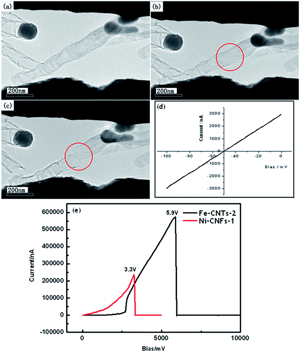 | ||
| Fig. 6 (a–c) TEM images of the thermal breakdown process of Fe-CNTs-2. (d) I–V curve of Fe-CNTs-2 after beam focusing. (e) Current density curves of Ni-CNFs-1 (red) and Fe-CNTs-2 (black). | ||
CNTs grown with Fe catalysts are also mounted between two electrodes by using the same method. The TEM image of a CNT on two electrodes is shown in Fig. 6(a) (Fe-CNTs-2). Focused beam is also used for the better connection. I–V curve of the CNT (after beam focusing) is shown in Fig. 6(d) and the measured resistance for the CNT is 33 kΩ. The resistivity of the CNT is about 3.73 × 10⁻⁴ Ω·m, which is two orders lower than that of the CNF. Several CNTs (five CNTs) have been measured showing similar resistivity. The results suggest that the present CNTs have better conductivity (or lower resistivity) than the CNFs prepared by similar method. The difference can be attributed to various factors. From the TEM images we know that CNF has a much thick wall than CNT. CNF also loses the coherent graphitic layers and show a stacking cone-like wall. The resistivity difference can be partly attributed to the morphology difference that a coherent graphitic may help for the conductivity. However, although both CNT and CNF are carbon based nanostructures, the composition and their electronic structure can be significantly different. As revealed by the XANES spectra, CNT shows much less oxidized groups than CNF, keeping a good carbon ring structure with less influence from oxidation. Thus a better conductivity can be expected. The heavily oxidized carbon structure as that in CNF may decrease the conductivity. The electrical properties can thus be related to the morphological structure and the electronic structure.
To confirm the relationship between the electronic structure and the electrical property, first-principle calculations were performed by using the software Dmol.3 A pristine armchair (5,5) single-walled carbon nanotube (SWCNT) with the diameter of 6.78 Å was used as a model. To compare with the oxidized state of SWCNT with various surface groups, the pristine SWCNT was then functionalized by four OH– groups, three CH3(CH2)2O– groups and four COOH– groups, respectively. The gradient-corrected functional developed by Perdew et al. (GGA-PBE) are used to describe the approximation of the exchange-correlation energy.18 The convergence criterions of total energy, force, and displacement are set to 10–6 Ha, 0.002 Ha Å−1, and 0.005 Å in the self-consistent calculations, respectively. A thermal smearing parameter 0.005 Ha was applied to accelerate the convergence of orbital occupation. The calculation model and results are shown in Fig. 7. The pristine (5,5) SWCNT keeps a Dirac cone with metallic characterization along the periodic direction (Fig. 7(a)). When decorated with various surface groups, all the modified SWCNT samples show a band gap in Fig. 7(c) and (d), which may lower the conductivity with worse performance. Actually, the oxidized CNTs were also reported in the literature to decrease the conductance due to a larger elastic mean free path of charge.19
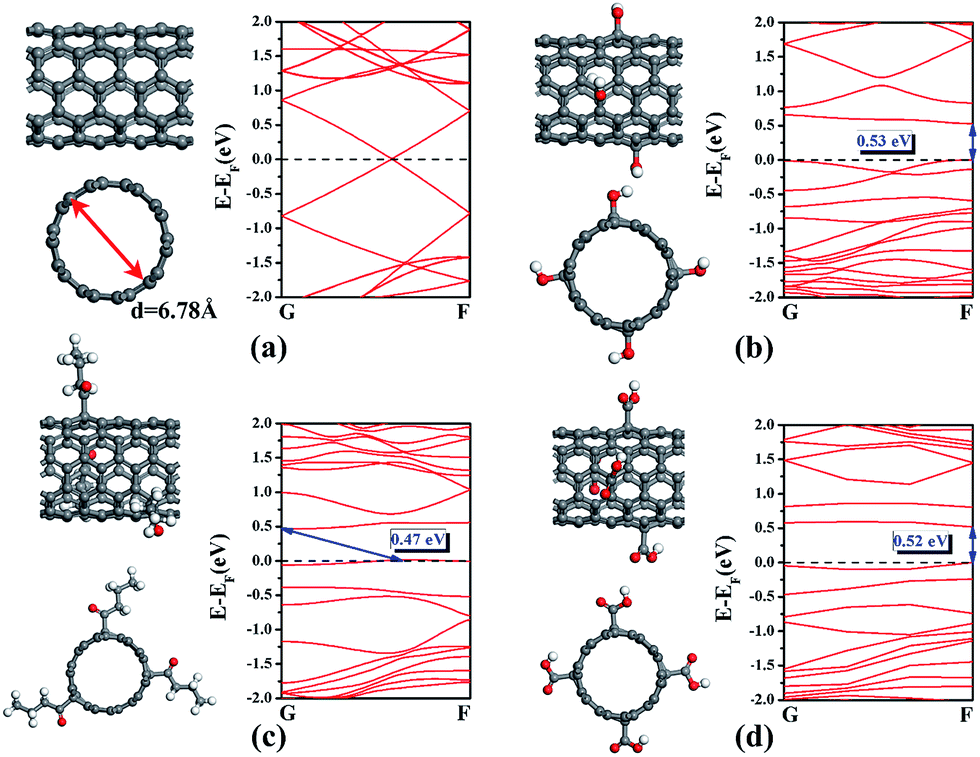 | ||
| Fig. 7 (a–d) The top view and side view of SWCNT (a), OH-SWCNT (b), CH3(CH2)2O-SWCNT (c) and COOH-SWCNT (d) and their corresponding band structure (the valance band maximum is set to zero). | ||
The stability of the CNT is also measured and the TEM images are shown in Fig. 6(b) and (c). The CNT break off until a bias of 5.9 V is applied, which is much higher than that for the CNF (Fig. 6(e)). The corresponding current density is 4.9 × 10¹⁰ A m−2, which is also much lager than that of CNF. Thus higher voltage and larger current can be applied on CNTs when they are used as parts of the nano-devices. Our results reveal the relationship of morphological structure, electronic structure and electrical transport property in carbon-based nanostructures such as CNFs and CNTs, which may favor the rational design of nano-devices.
4. Conclusions
The electronic structures of CNTs and CNFs with different morphological structures have been investigated by using XANES, which reveals that CNTs have much oxidized groups than CNFs. The electrical transport properties have been measured and the resistivity of single CNT is 3.73 × 10⁻⁴ Ω·m, which is 2 orders lower than that of CNFs (1.35 × 10⁻² Ω·m). The breakdown bias of single CNT has also been tested which is much higher than that of single CNF, indicating higher voltage and larger current can be applied on CNTs before thermal breakdown. The different electrical properties can be attributed to the different morphology and the electronic structure as revealed by XANES. Our results offer a good example to examine the relationship of morphological structure, electronic structure and electrical transport property in carbon nanomaterials, which will be certainly useful in the applications of nano-devices.Acknowledgements
Research at CLS is supported by NSERC, NRC, CIHR, and the University of Saskatchewan. We acknowledge the National Natural Science Foundation of China (No. 91333112, U1432249). This is also a project supported by Collaborative Innovation Center of Suzhou Nano Science & Technology, Soochow University-Western University Centre for Synchrotron Radiation Research, the Priority Academic Program Development of Jiangsu Higher Education Institutions, and Qing Lan Project.Notes and references
- R. H. Baughman, A. A. Zakhidov and W. A. de Heer, Science, 2002, 297, 787 CrossRef CAS PubMed.
- A. Javey, J. Guo, D. B. Farmer, Q. Wang, E. Yenilmez, R. G. Gordon, M. Lundstrom and H. J. Dai, Nano Lett., 2004, 4, 1319 CrossRef CAS.
- Y. Awano, IEICE Trans. Electron., 2006, 89, 1499 CrossRef.
- J. Li, H. T. Ng, A. Cassell, W. Fan, H. Chen, Q. Ye, J. Koehne, J. Han and M. Meyyappan, Nano Lett., 2003, 3, 597 CrossRef CAS.
- Z. E. Horvath, A. A. Koos, K. Kertesz, G. Molnar, G. Vertesy, M. C. Bein, T. Frigyes, Z. Meszaros, J. Gyulai and L. P. Biro, Appl. Phys. A: Mater. Sci. Process., 2008, 93, 495 CrossRef CAS.
- Z. Ren, Z. Huang, J. Xu, J. Wang, P. Bush, M. Siegal and P. Provencio, Science, 1998, 282, 1105 CrossRef CAS PubMed.
- H. T. Ng, B. Chen, J. E. Koehne, A. M. Cassell, J. Li, J. Han and M. Meyyappan, J. Phys. Chem. B, 2003, 107, 8484 CrossRef CAS.
- A. M. Cassell, Q. Ye, B. A. Cruden, J. Li, P. C. Sarrazin, H. T. Ng, J. Han and M. Meyyappan, Nanotechnology, 2003, 15, 9 CrossRef.
- M. Kabir, R. E. Morjan, O. Nerushev, P. Lundgren, S. Bengtsson, P. Enokson and B. Campbell, Nanotechnology, 2005, 16, 458 CrossRef CAS.
- A. Kawabata, S. Sato, T. Nozue, T. Hyakushima, M. Norimatsu, M. Mishima, T. Murakami, D. Kondo, K. Asano and M. Ohfuti, Proceedings of the IEEE 2008 International Interconnect Technology Conference, 2008, p. 237 Search PubMed.
- Z. J. Han and K. Ostrikov, J. Am. Chem. Soc., 2012, 134, 6018 CrossRef CAS PubMed.
- X. H. Sun, K. Li, R. Wu, P. Wilhite, T. Saito, J. Gao and C. Yang, Nanotechnology, 2009, 21, 045201 CrossRef PubMed.
- A. Kuznetsova, I. Popova, J. T. Yates, M. J. Bronikowski, C. B. Huffman, J. Liu, R. E. Smalley, H. H. Hwu and J. G. G. Chen, J. Am. Chem. Soc., 2001, 123, 10699 CrossRef CAS PubMed.
- Y. Tang, P. Zhang, P. Kim, T. Sham, Y. Hu, X. Sun, N. Wong, M. Fung, Y. Zheng and C. Lee, Appl. Phys. Lett., 2001, 79, 3773 CrossRef CAS.
- J. Zhong, J. J. Deng, B. H. Mao, T. Xie, X. H. Sun, Z. G. Mou, C. Hong, P. Yang and S. D. Wang, Carbon, 2012, 50, 335 CrossRef CAS.
- J. Zhong, H. Zhang, X. H. Sun and S. T. Lee, Adv. Mater., 2014, 26, 7786 CrossRef CAS PubMed.
- X. Lv, J. Deng, J. Wang, J. Zhong and X. H. Sun, J. Mater. Chem. A, 2015, 3, 5183 CAS.
- J. P. Perdew, K. Burke and M. Ernzerhof, Phys. Rev. Lett., 1996, 77, 3865 CrossRef CAS PubMed.
- A. Lopez-Bezanilla, F. Triozon, S. Latil, X. Blase and S. Roche, Nano Lett., 2009, 9, 940 CrossRef CAS PubMed.
| This journal is © The Royal Society of Chemistry 2017 |