
 Open Access Article
 This Open Access Article is licensed under a Creative Commons Attribution-Non Commercial 3.0 Unported Licence
Manipulating intrinsic behaviors of graphene by substituting alkaline earth metal atoms in its structure
Muhammad Rafique ab,
Yong Shuai*a,
He-Ping Tana and
Muhammad Hassana
ab,
Yong Shuai*a,
He-Ping Tana and
Muhammad Hassana
aSchool of Energy Science and Engineering, Harbin Institute of Technology, 92 West Dazhi Street, Harbin 150001, PR China. E-mail: shuaiyong@hit.edu.cn
bMehran University of Engineering and Technology, S.Z.A.B Campus, Khairpur Mir's, Sindh, Pakistan
First published on 14th March 2017
Abstract
In this paper, the structural, electronic, magnetic and optical properties of alkaline earth metal (AEM) atom-doped monolayer graphene are investigated using first-principles calculations. It is found that, Be, Mg and Ca atom substituted graphene structures exhibit half metallic behavior with 0.00 μB, 1.86 μB, and 4.00 μB magnetic moments, respectively. While, Sr and Ba atom-doped graphene structures display indirect band gap semiconductor behavior with 3.16 μB and 0.46 μB magnetic moments, respectively. All the impurity atoms are tightly bonded with graphene, having significant formation energy and the direction of charge transfer is from AEM atoms to the graphene. Upon analyzing density of states plots we found that the s and p orbitals of impurity atoms give rise to magnetic moments in graphene complexes. The optical properties for pure graphene and AEM atom-doped graphene complexes have been calculated within the random phase approximation (RPA) approach. The absorption coefficient and reflectivity plots for doped graphene complexes are calculated and compared to the results obtained for pure graphene. A significant change in optical properties specifically in the absorption spectrum of graphene is obtained after AEM atom substitution. It is found that AEM atom substitution into graphene produces an increase in the absorption spectrum in the energy range of 0 to 3 eV and a reduction in absorption peaks at a 14 eV energy level. In addition, a third minimum absorption peak appears in the energy interval of 7 to 11 eV, which is not present in the absorption spectrum of pure graphene. A significant red shift in absorption towards the visible range of radiation is also obtained. An increase in reflectivity peak in the low energy region is observed after AEM atom substitution into graphene. We believe that our results are suitable for further experimental exploration and useful for graphene based spintronic and optoelectronic devices.
1. Introduction
Since the discovery of this unique two-dimensional (2D) material graphene,1–3 a significant amount of experimental and theoretical work has been attributed to the possibility of manipulating the properties of this fascinating material. A straightforward way to obtain this goal is to functionalize graphene through substitutional doping, some carbon (C) atoms in the graphene sheet are replaced with foreign atoms and their effects are investigated.4–6 These studies depict that the band structure of graphene is sensitively dependent on the nature of dopant atoms. Given the unique structure of graphene, with planar sp2 bonding and π bonding with perpendicular pz orbitals, it is a nonmagnetic semimetal with a linear dispersion of energy near the Fermi energy (EF) level.3In order to broaden the applications of graphene as a magnetic material, to be used for novel spintronic devices, various approaches have been utilized to functionalize graphene for introducing ferromagnetism behavior in graphene.7–9 For example, producing defects in graphene layer by electron or ion beam10–12 can produce magnetism in graphene. Metal adatoms on graphene, silicene and nanotubes has been widely analyzed for ferromagnetism behaviors by first-principles calculation.13–16 Recently, there are two main approaches widely utilized for substituting metal adatoms into graphene. One approach is to adsorb metal adatoms on graphene surface17 and the other is to incorporate foreign metal atoms into graphene vacancies, namely single vacancy (SV) or di-vacancy (DV). Previous studies reveal that the binding energies obtained for foreign atoms embedded into graphene vacancies are far better than the calculated binding energies of metal atoms adsorbed on the graphene surfaces. In addition to that, foreign atom doped graphene complexes are suitable for graphene-based devices operating at room temperatures and above, in comparison to the metal atoms adsorbed graphene structures.18–20 Recently, Minglei Sun et al.21 performed first-principles calculations on AEM atom adsorption on graphene. Authors reported that, AEM atom adsorption can introduce significant ferromagnetism properties and makes graphene semimetal or half metallic depending upon adsorbate atom type. However, this study is focused on AEM atom adsorption, therefore, we try to analyze ferromagnetism behavior and calculate electronic properties after AEM atoms substitution into graphene layer.
Similarly, graphene can be optically contrasted from the substrate22,23 which can lead to luminescence through chemical and physical treatments23–25 which makes this material an ideal choice for photonic and optoelectronic devices.26 Since, pure graphene is transparent in the visible region of spectrum, so in order to obtain graphene based optoelectronic devices to be functional, it is very critical to manipulate optical properties of graphene to make it able to absorb specific wavelength of spectra. Optical properties of graphite and graphene has been comprehensively investigated by Sedelnikova et al.27 and Marinopoulos et al.26 Marinopoulos et al. have investigated the absorption spectrum for different values of c/a ratio and compared it with that of flat boron nitride (BN) sheet. Similarly, Eberlein et al.28 performed experimental spectroscopy of graphene along with first-principles calculations of the low loss function. Since most of the work in these studies is attributed to analyzing optical properties of pure graphene but no systematic and in-depth study using first-principles calculations to determine the effect of foreign-atom doping on the optical properties of graphene has been reported previously. So far, a systematic and thorough study on substitution of AEM atoms in graphene remains scattered and unfinished. Therefore, a comprehensive theoretical study is timely at present.
In this work, we analyzed the trends in structural parameters, electronic, magnetic and optical properties of AEM atoms (Be, Mg, Ca, Sr and Ba) doped graphene structures by means of first-principles calculations. We choose different AEM atoms for this study, using each individual AEM atom as the dopant due to their electron-rich characters i.e. containing 2 electrons in their valence shells. Hence, these AEM atoms can significantly alter the electronic structure of graphene and induce band gap. In addition, the valence electrons of AEM atoms can be the reason for introducing ferromagnetism in graphene. Our work is organized as follows. In Section 2, computational methods are described. Our main obtained numerical results and discussions are elaborated in Section 3. Finally, in Section 4, we provide the summary with some general conclusions.
2. Details of computation
The structural, electronic, magnetic and optical properties of alkaline earth metal (AEM) atom-doped monolayer graphene were investigated by density functional theory (DFT), in the generalized-gradient approximation (GGA) implemented in Vienna Ab initio Simulation Package (VASP).29,30 In which the projector augmented wave (PAW) potentials31 with Perdew–Burke–Ernzerhof (PBE) functional32 of exchange-correlation are utilized. The DFT method is known to be one of the most accurate methods for calculating electronic structure of solids.33–39 All the results were obtained in spin-polarized condition except band structure calculations. A kinetic energy cutoff of 500 eV was used for wave function expansion. Our structure model consists of a 4 × 3 monolayer graphene supercell (23 carbon atoms with 1 impurity atom) with a vacuum layer of 15 Å in Z-direction to eradicate the interaction between adjacent layers. Since the convergence with respect to the number of K-points was very critical to obtain accurate results, hence we utilized a 9 × 9 × 1 Γ-centered k-point mesh for Brillouin zone (BZ) sampling. All the structures were fully optimized until the Hellmann–Feynman forces less than 0.01 eV Å−1 and the total change in energy less than 10−6 eV was achieved. Gaussian smearing method was utilized to deal with the partial occupancies.3. Results and discussions
3.1. Formation energy, structural and magnetic properties
First question one has to address is, of course, weather the AEM atom substitution in graphene is stable or not. In order to verify the stability of our AEM atom-doped monolayer graphene structures, we calculated the formation energy for each structural model. The formation energy (EF) for AEM atom-doped graphene can be calculated as,18 EF = Etotal − (Egraphene + Eatom). Where, Etotal is the total energy of the graphene with AEM impurity atom, Egraphene is the total energy of graphene with vacancy and Eatom is the energy of individual AEM atom, respectively. The calculated formation energies were found to be, −5.868 eV, −4.448 eV, −6.045 eV, −8.18 eV and −10.61 eV for Be, Mg, Ca, Sr and Ba atom-doped graphene structures respectively. Given formation energy values indicate that Be, Mg and Ca atom substitution into graphene is more thermodynamically favorable in comparison to Sr and Ba atom substitution. This is due to the larger atomic radii of Sr and Ba atom, which causes larger local distortion in the graphene in comparison to Be, Mg and Ca atom-doped graphene structures. These results are in consensus with the previous studies available.21,40In this work, different AEM atoms (Be, Mg, Ca, Sr and Ba) were substituted into monolayer graphene as shown in Fig. 1. Fig. 1(a) and (b) show the top and side views of AEM atom doped 4 × 3 monolayer graphene supercell (23 carbon atoms with 1 impurity atom), respectively. In this section, we try to investigate the effect of AEM atom doping on structural and magnetic properties of graphene. We performed geometry optimization for all the AEM atom-doped graphene complexes until it reached the required accuracy. In order to determine the changes in bond lengths between C–C atoms and the change in lattice constant after geometry optimization process, the C atoms around the dopant impurity atoms were not fixed during calculations. The C atoms were allowed to relax during geometry optimization.
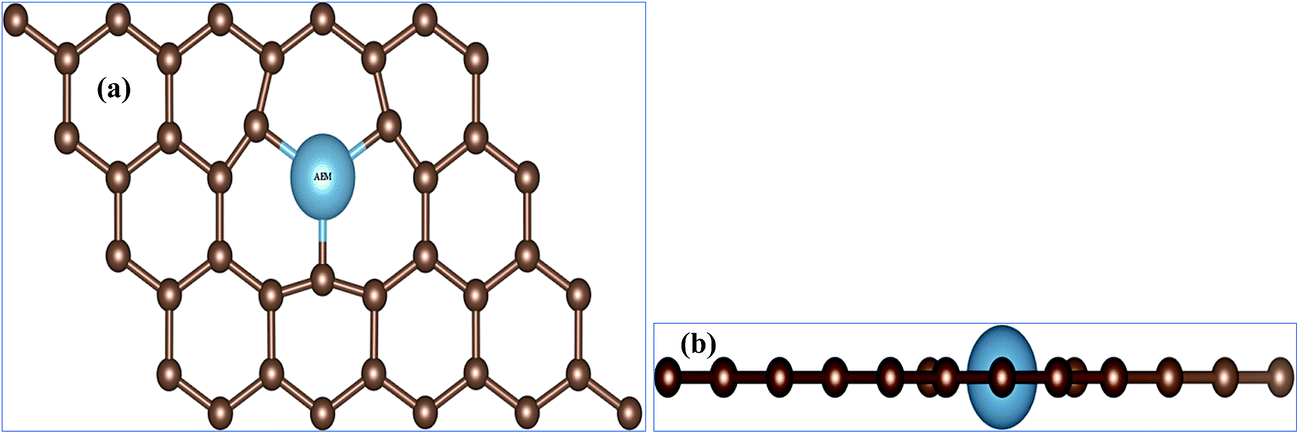 | ||
| Fig. 1 (a) Top view and (b) side view of atomic structures of AEM atom embedded into monolayer graphene. The small brown balls represents C atoms and big ball represents dopant AEM atom. | ||
Fig. 2 represents bond distances of AEM–C and bond distances of C–C atoms after geometry relaxation of AEM atoms embedded into monolayer graphene. It was found that, after AEM atom-doping into graphene, the 2D structure of the graphene complexes were retained during geometry optimization. When AEM atoms are substituted into graphene, they bind with neighboring three C atoms through sp2 hybridization. Due to larger covalent radii of AEM atoms i.e. (Be (102 pm), Mg (139 pm), Ca (171 pm), Sr (185 pm) and Ba (196 pm)) compared to covalent radius of C (75 pm) atom, a substantial change in bond length occurs. It is also found that the AEM atoms with larger covalent radii caused sufficient local deformation in comparison to the AEM atoms with smaller covalent radii. The bond distances of C–C atoms around the AEM impurity atoms were found to be equal at in range of 1.28–1.38 Å and the change in C–C bond lengths were in between 0.14 Å to 0.04 Å, depending upon the size of covalent radius of impurity atom. In addition, the Jahn–Teller distortion lowered the local symmetry from the D3h symmetry of graphene to C3v, Cs or Ci symmetry of the AEM atom-doped graphene. This prediction is consistent with the fact that the three equatorial AEM–C bond distances are not similar, as presented in Fig. 2. We compared structural parameters of Be atom-doped graphene with the previous study carried on Be atom doping into graphene,40 in order to verify our calculation method. The change in bond length between Be and host C atom (dBe–C) and the change in bond length between C–C atom (dC–C) are given in Table 1. The structural parameters calculated for Be atom-doped graphene are in complete agreement with the results provided in ref. 40 as presented in Table 1. This comparison depicts that our employed computational method and structural model used in this work is enough accurate to carry out further calculations for other given models present in our work. The structural parameters calculated for remaining AEM atom-doped graphene are consistent with the previous studies carried on AEM atom-doped graphene.41–43
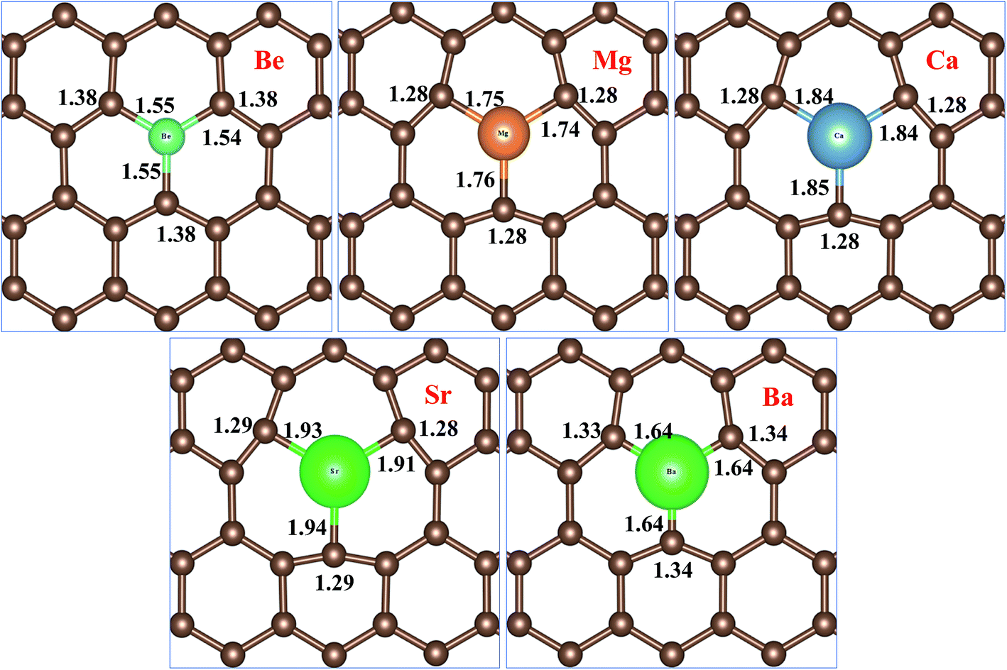 | ||
| Fig. 2 Top views of atomic structures of AEM atoms incorporated into monolayer graphene showing bond lengths of AEM–C and C–C atoms. Bond length is shown in Å. | ||
| Study | dBe–C (Å) | dC–C (Å) |
|---|---|---|
| Our work | 1.55 | 1.38 |
| Saif Ullah et al.40 | 1.56 | 1.38 |
Table 2 given below lists the average equatorial bond distances between AEM–C atoms, bond distances between C–C atoms, the total magnetization μtot of the supercell and the magnetic moment of individual AEM atoms μAEM for all AEM atom-doped graphene complexes.
| Impurity | μtot, in μB | μAEM, in μB | dAEM–C Å | dC–C Å |
|---|---|---|---|---|
| Be | 0.00 | 0.00 | 1.55 | 1.38 |
| Mg | 1.86 | 1.34 | 1.75 | 1.28 |
| Ca | 4.00 | 2.19 | 1.84 | 1.28 |
| Sr | 3.16 | 1.52 | 1.93 | 1.29 |
| Ba | 0.46 | 0.26 | 1.64 | 1.34 |
The total magnetic moments μtot of the AEM atom-doped graphene complexes and magnetic moments of individual AEM atoms μAEM listed in Table 2 illustrate that, larger magnetic moments per supercell can be achieved by substituting AEM atoms in graphene, except Be atom-doped graphene structure. Obtained total magnetic moments for different AEM atoms embedded graphene structures are 0.00 μB, 1.86 μB, 4.00 μB, 3.16 μB and 0.46 μB for Be, Mg, Ca, Sr and Ba atom-doped graphene complexes, respectively. In order to further understand the ferromagnetism behavior, we analyzed the magnetic coupling behavior for the AEM atom-doped graphene complexes. Fig. 3 presents the spin densities (ρ↑ − ρ↓) of different AEM (Mg, Ca, Sr and Ba) atom-doped graphene structures. We neglected spin density of Be atom-doped graphene structure due to its weak ferromagnetism coupling with the graphene supercell as described by its 0.00 μB magnetic moment. From the spin density diagrams shown in Fig. 3, we can predict that all the AEM atoms embedded into graphene structures demonstrate similar magnetic coupling behavior between substituted AEM atom and the graphene layer. Significant magnetic coupling was observed between impurity AEM atom and three neighboring C atoms. It was also observed that after AEM atom substitution, the change in spin density in the graphene was not localized at the defect site but it was distributed along the graphene plane. Due to smaller magnetic moment of Ba atom-doped graphene complex, positive spin density was concentrated at the Ba atom. On the other hand, C atoms of Ba-doped graphene contained smaller positive spin density in comparison to C atoms of Mg, Ca and Sr atom-doped graphene structures. This unique phenomenon of spin density of Ba atom-doped graphene can be attributed to the unstable interaction between Ba and C atoms as indicated by formation energy results. Smaller atomic interaction results in lower ferromagnetism coupling, thereby restricting the spin density at the impurity Ba atom site. It is also found that the direction of spin polarization on AEM atoms and neighboring C atoms is antiparallel in case of Mg, Ca, Sr and Ba atom-doped graphene structures as shown in Fig. 3, respectively. Our obtained results for ferromagnetism behavior of AEM atom-doped graphene structures are consistent with the previous reports available.21,41,44
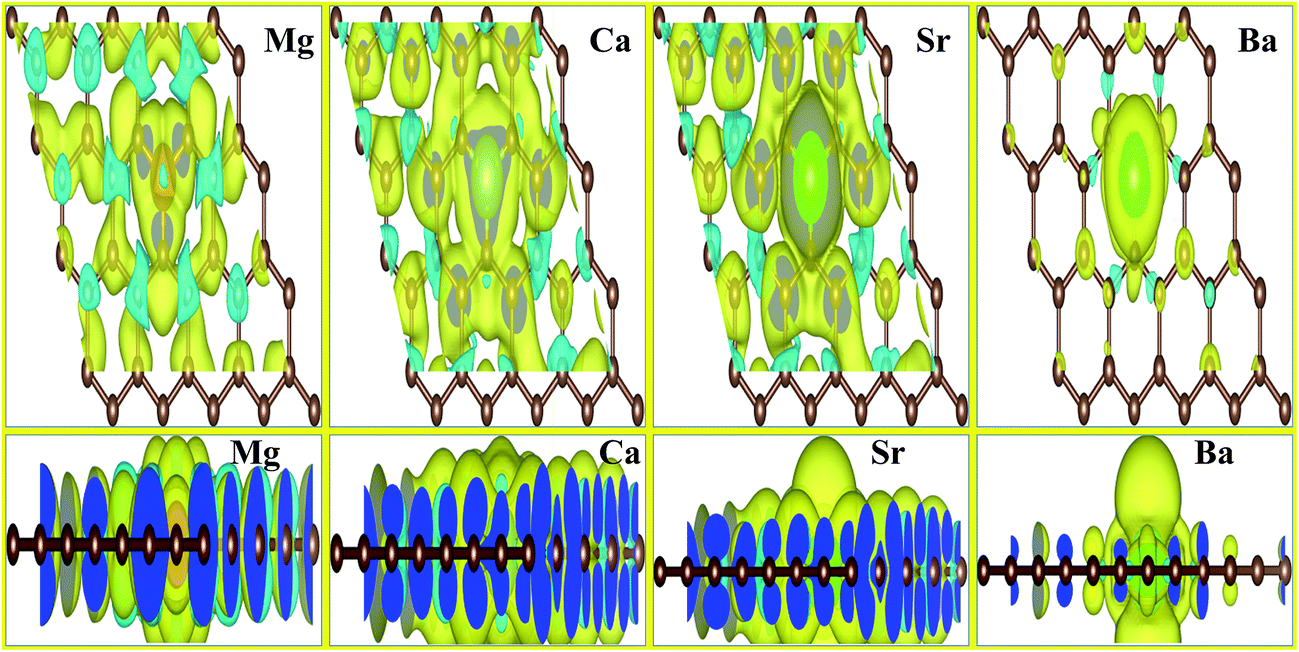 | ||
| Fig. 3 Top and side views of spin density for AEM atom-doped into a (4 × 3) graphene supercell. Yellow and cyan isosurfaces represent positive and negative spin densities, respectively. The isosurfaces value is 0.0003 e Å−3. | ||
We also investigated the charge transfer behavior using Bader analysis45,46 for all AEM atom-doped graphene structures. The charge density difference can be defined as ΔρAEM = ρAEM graphene − ρgraphene − ρAEM. Where ρAEM graphene, ρgraphene and ρAEM terms describe the charge density of AEM atom-doped graphene, charge density of graphene with vacancy and charge density of individual AEM atom, respectively. The top view of charge density difference diagrams for all AEM (Be, Mg, Ca, Sr an Ba) atom-doped graphene structures with a charge density iso-surface value of 0.01 e Å−3 are shown in Fig. 4, respectively. Yellow regions (i.e. 0.01 e Å−3) in Fig. 4 indicate gain of electron, while cyan regions (i.e. 0.01 e Å−3) indicate loss of electron.
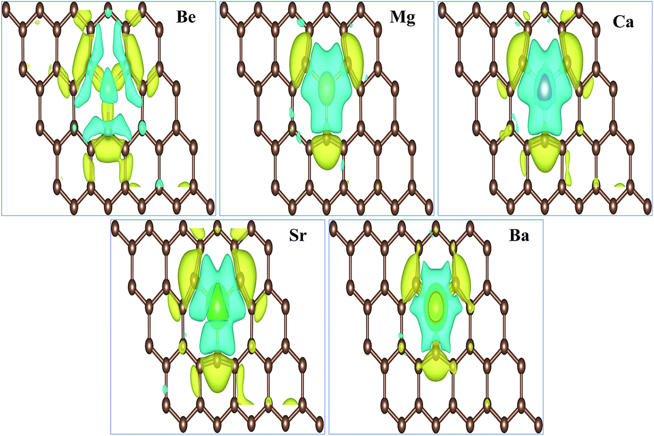 | ||
| Fig. 4 Top views of charge density difference diagrams for AEM atom-doped (4 × 3) graphene supercell structure. Yellow and cyan isosurfaces (0.01 e Å−3) correspond to electron gain and electron loss behavior, respectively. | ||
In case of Mg, Ca and Sr atom-doped graphene structures, the charge density around the impurity AEM atoms is decreased as indicated by cyan iso-surface and the charge density around the C atoms directly bonded to impurity atoms is increased as indicated by yellow iso-surface. This phenomenon suggests that the direction of charge transfer is from AEM atoms to the graphene layer. This behavior indicates that the interaction between AEM and C atoms is ionic in nature because Mg, Ca and Sr atoms depict loss of electron and C atoms present around the impurity atom show gain of electron.
For Be atom-doped graphene structure, charge density in the vicinity of Be and C atoms is increased as depicted by yellow iso-surface. However charge density on Be atom and three C atoms is decreased as indicated by cyan iso-surface. This behavior suggests that the interaction between Be and C atoms is covalent in nature.
For Ba atom-doped graphene structure, charge density in the vicinity of Ba and C atoms is reduced as depicted by cyan iso-surface. However charge density on Ba and three C atoms is increased as indicated by yellow iso-surface. This behavior suggests that the interaction between Ba and C atoms is also covalent in nature. Our obtained results for charge transfer are consistent with the previous studies available.41,44,47
3.2. Electronic properties
In this section, we try to investigate the effects of AEM atom doping on the electronic properties of graphene. Band structure and density of states (DOS) plots were calculated for all AEM atom-doped monolayer graphene structures. Twenty points are collected along each high symmetry lines using path Γ–M–K–Γ in the irreducible Brillouin zone for band structure calculation, in order to obtain the band structure with very fine grid. Total and projected density of states (PDOS) is also calculated for all AEM atom-doped graphene structures using a 11 × 11 × 1 Gamma centered Brillouin-zone sampling and the energy eigenvalues are smeared with Gaussians of width 0.2 eV. We used spin polarized mode for calculating PDOS plots.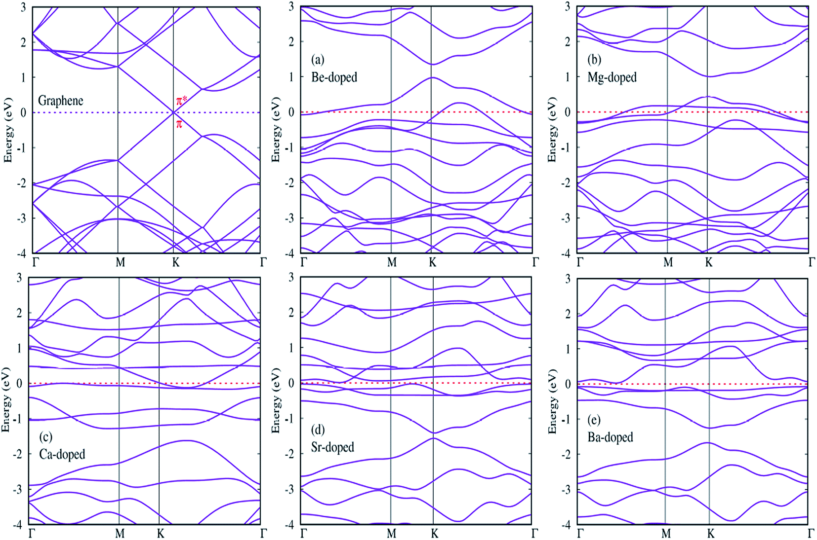 | ||
| Fig. 5 Band structure diagrams for AEM atom-doped monolayer (4 × 3) graphene supercell structure. | ||
Since we know that AEM atoms have excess of charge, hence these atoms can be regarded as accepter-donor impurities, depending upon the nature of dopant atom. In case of Be and Mg atom substitution, the Fermi energy level (EF) shifts into valence band and the Dirac cone moves to conduction band. Be and Mg atom doping can be regarded as p-type doping. After Be and Mg atom substitution, a band gap of approximately 0.3 eV and 0.6 eV appears at high symmetric K-point as shown in Fig. 5(a) and (b), respectively. Be and Mg doped graphene structures exhibit metallic behavior as some surface states are present at the Fermi level. In case of Ca, Sr and Ba atom-doped graphene structures, the Fermi energy level (EF) shifts into conduction band and the Dirac cone moves to valence band, hence Ca, Sr and Ba atom-doping can be regarded as n-type doping. Similar to Be and Mg atom substitution, Ca atom-doped graphene also displays metallic behavior due to some surface states present at the Fermi level as shown in Fig. 5(c). While Sr and Ba atom-doped graphene structures display indirect band gap semiconductor behavior with a band gap of approximately 0.2 eV and 0.8 eV, respectively as shown by Fig. 5(d) and (e). Some surface states induced by impurity atoms near the top of the valence band and bottom of the conduction band are observed as shown in Fig. 5(a)–(e). Clearly, these impurity states appear due to hybridization between s and p orbitals of AEM atoms and p orbitals of C atoms. The emergence of finite band gap in the band structure diagrams of AEM atom-doped graphene complexes can be attributed to the local distortion of the graphene induced by impurity atoms which break the symmetry of the sub lattices of graphene. Our obtained results are consistent with previous works.40–42,50
After calculating the band structure diagrams for different AEM atom-doped graphene structures, we try to compare our obtained results with the previous studies.51–54 These studies depict the band gap of graphene doped with different impurity atoms and the effect of change in concentration of dopants on the band gap value.
Table 3 given below lists the band gap (eV) of graphene doped with boron (B) and nitrogen (N) atoms with varying number of dopant atoms. The band gap values presented in Table 3 clearly reveal that the value of band gap induced in graphene is directly proportional to the concentration of dopant atoms. However, if we compare our results of single AEM atom doped graphene to the single B or N atom doped graphene, we can clearly observe that the AEM atom doped graphene has larger band gap value as compared to individual B or N atom doped graphene. This increase in band gap can be attributed to the increased number of valence electrons present in AEM atom outer shell. This kind of results can bring deeper understanding into the interaction between AEM atoms and graphene.
Next, we try to examine the spin polarized total density of states (TDOS) and projected density of states (PDOS) plots for all the AEM atom-doped graphene structures in order to comprehend the origin of magnetism after AEM atom-doping into graphene. TDOS and PDOS on the AEM atom sp orbitals and adjacent C atom p orbital for all AEM atom-doped graphene structures are shown in Fig. 6(a)–(e), respectively. Given PDOS plots of AEM atom-doped graphene structures illustrate only s and p orbitals of AEM atoms while neglecting d orbitals. Previous studies reveal that only s orbitals of AEM atoms can be responsible for introducing ferromagnetism in graphene.21,50 Therefore, TDOS and PDOS on AEM atom sp orbitals were produced. The Fermi energy level (EF) is shown at 0 eV energy level by a vertical thin grey line appearing in the given PDOS plots. After AEM (Be, Mg, Ca, Sr and Ba) atom substitution into graphene, some impurity states appear near the top of the valence band and the bottom of conduction band in the respective PDOS plots presented in Fig. 6(a)–(e), respectively. These impurity states observed at the Fermi level appear due to the occurrence of robust hybridization between sp orbitals of AEM atoms and p orbitals of C atoms. Different s and p orbitals of AEM atoms and p orbitals C atoms are described by labeled color lines in the given PDOS plots. Since we know that Mg, Ca and Sr atom-doped graphene structures have 1.86 μB, 4.00 μB and 3.16 μB magnetic moments, respectively. Therefore their s and p orbitals contain larger spin polarization as shown in Fig. 6(b)–(d), respectively. On the other hand Be and Ba atom-doped graphene structures have 0.00 μB and 0.46 μB magnetic moments, respectively, hence their s and p orbitals contain less spin polarization as shown in Fig. 6(a) and (d), respectively.
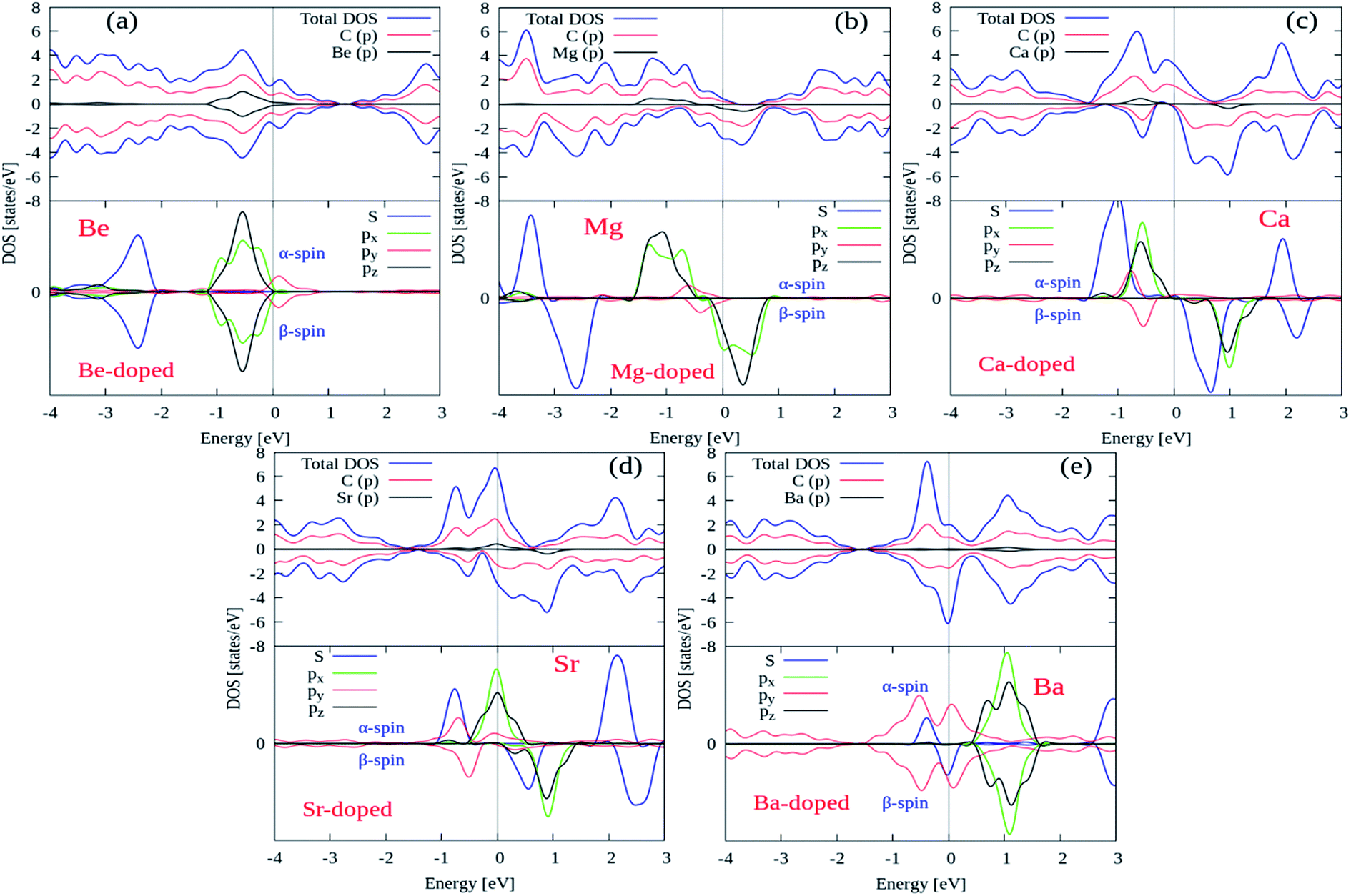 | ||
| Fig. 6 Total and projected densities of states (DOSs) of AEM atoms incorporated into monolayer graphene. Fermi level is indicated by the vertical solid grey line at 0 eV energy level. | ||
From the given PDOS plots we can further predict that the s and p orbitals namely (s, px, py and pz) of AEM atoms give rise to magnetic moments of AEM atoms-doped graphene structures. An important phenomenon to understand here is that the emergence of band gap in spin up state channel and spin down state channel is at different energy levels attributed to the polarization of spin state bands. From our obtained results, we can predict that AEM atom-doped graphene complexes can be practical for the concept of spintronics. These obtained results further suggest that 2D magnetic semiconductors can be synthesized by doping AEM atoms into monolayer graphene.
3.3. Optical properties of AEM atom-doped graphene
Lastly, we calculated optical properties using DFT within the Random Phase Approximation (RPA)55 approach. In this approach local fields effects are neglected and interband transitions are included, so there can be some inaccuracy in dielectric function results at low energies. In order to calculate absorption coefficient ‘α’ and reflectivity ‘R’, we need dielectric tensor values. Dielectric constant is the sum of real and imaginary part i.e. ε = ε′ + ε′′ together. The imaginary part can be calculated by the summation of empty states using following equation.
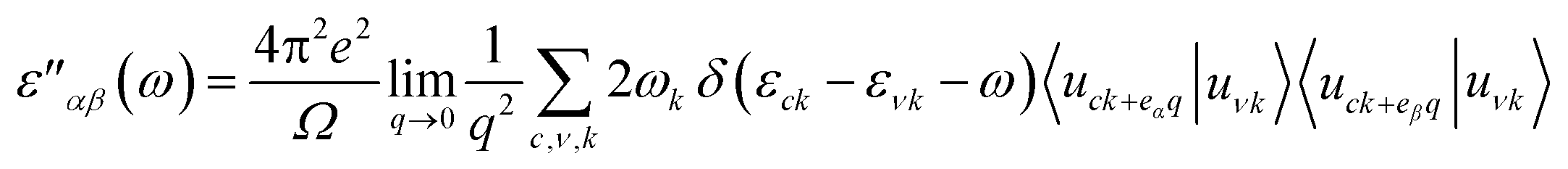 | (1) |
The real part of dielectric tensor is obtained by using Kramers–Kronig transformation,
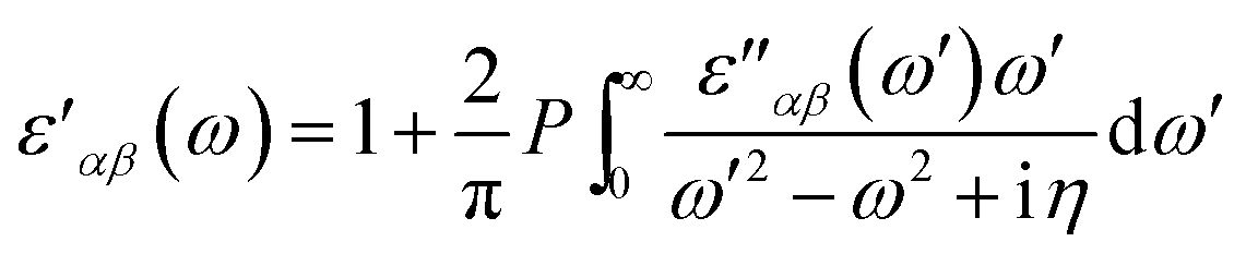 | (2) |
After getting dielectric tensor values we can easily get absorption coefficient ‘α’ and reflectivity ‘R’. The method to calculate these optical parameters is fully explained in ref. 26.
Firstly, we calculated the absorption coefficient and reflectivity plots of pure graphene. Our values obtained for the optical properties of pure graphene are in consensus with the results of previous studies.27,52,56,57 However minor variations in the results can be attributed to the difference between the size of supercell and the utilization of k-point mesh. We utilized 13 × 13 × 1 Γ-centered Brillouin-zone sampling for calculating optical properties, specifically absorption coefficient and reflectivity plots.
The absorption coefficient plots for pure graphene and AEM (Be, Mg, Ca, Sr and Ba) atom-doped graphene structures are shown in Fig. 7(a) and (b) and the comparison is made among all the structural models. The energy interval was set from 0 to 25 eV for calculating the absorption coefficient, in order to determine the overall effect for AEM atom substitution on absorption spectrum of graphene. In the absorption spectrum of pure graphene, there are two main absorption coefficient peaks namely ‘A’, ‘B’ appearing at energy levels of 4.5 eV, 14 eV, with an intensity of approximately 3800 cm−1 and 9000 cm−1 as shown in Fig. 7(a), respectively. These calculations are consistent with previous studies.52,56 If we observe closely the absorption spectrum of pure graphene given in Fig. 7(a), we can predict that pure graphene has zero absorption in the energy levels of 0 eV to 0.5 eV and also from 7 eV to 11 eV. These findings are clearly indicated in the regions lying in between two dashed red lines vertically appearing at 5 eV and 11 eV energy levels. However, after AEM atom substitution in graphene leads to appearance of absorption spectrum starting from 0 eV, which suggests that AEM atom substitution introduces red shift in the absorption spectrum of pure graphene as clearly shown by Fig. 7(a) and (b), respectively. Similarly, as described earlier that graphene has almost zero absorption in energy level of 7 eV to 11 eV, however a third important absorption peak namely ‘C’ appears in the absorption spectrum after AEM atom substitution in graphene. The appearance of third peak ‘C’ suggests that there is increase in absorption coefficient value in the 7 eV to 11 eV energy region as shown in Fig. 7(a) and (b), respectively. An important factor to note here that, in case of AEM atom substitution, the maximum absorption peak ‘B’ which appears at 14 eV in case of pure graphene is reduced to lower values and the minimum absorption peak ‘A’ appearing at 4.5 eV is shifted to lower energy regions. In summarized way one can define that AEM atom substitution into graphene, produces overall reduction in absorption coefficient however a red shift occurs in absorption spectrum at visible energy region.
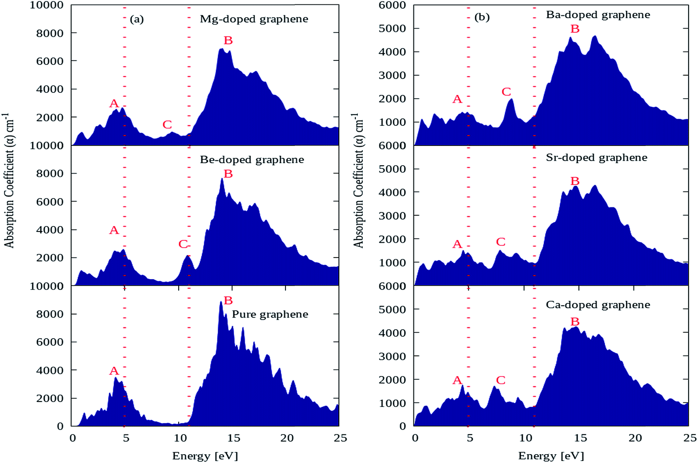 | ||
| Fig. 7 Absorption coefficient of (a) pure, Be, Mg atom-doped and (b) Ca, Sr and Ba atom-doped graphene. | ||
As described earlier that, pure graphene absorption spectrum contains two main peaks namely ‘A’ and ‘B’ at energy levels of 4.5 eV and 14 eV, respectively. However, after AEM atom substitution into graphene, a third peak namely ‘C’ appears in the absorption spectrum between 7 eV to 11 eV energy region. Fig. 8 shows the absorption spectrum of pure graphene (gp) and AEM (Be, Mg, Ca, Sr and Ba) atom-doped graphene in the energy region for 0 eV to 12 eV. We selected this energy interval in order to fully comprehend the effect of AEM atom substitution on absorption spectrum of graphene during low energy region. As shown in Fig. 8, the absorption spectrum of graphene has no value till 1 eV, however it gradually increases, manifests a sharp rise at 3 eV, attains a maximum value at approximately 4.8 eV and then depicts an asymmetric line shape.58–60 In addition, after AEM atom substitution, absorption coefficient quantity starts from 0 eV energy. There are two very interesting factors revealed in the absorption spectrum after AEM-atom substitution in graphene. First, the overall absorption profiles are similar, however, the first absorption peak observed in pure graphene at 4.8 eV energy level, shifts to lower energy level by amount of 0.1–0.3 eV approximately in case of AEM atom-doped graphene. This shift in the absorption spectrum is the consequence of incorporation of electron-rich AEM atoms in the aromatic ring of graphene. In case of Be and Mg atom-doped graphene, the absorption peak at 4.8 eV has higher intensity in comparison to pure graphene as shown in Fig. 8, respectively. Second, pure graphene has almost zero absorption in the energy interval of 7–11 eV. However, after AEM atom substitution in graphene, absorption coefficient peak appears in 7–11 eV energy region. Be, Ca and Ba atom-doped graphene has a significant peak at 11 eV, 7 eV and 9 eV with intensity of 2200, 2000 and 1700 respectively, as shown in Fig. 8, respectively. The appearance of this third peak is attributed to the effects of impurity defects and disorders produced in the graphene by AEM atom substitution. Due to access of charge in the AEM atoms present in the graphene layer, some negative charges are transferred onto graphene, which leads to modification of the electronic structure of graphene and thereby causing alteration in the optical absorption spectrum as described by Fig. 8, respectively.
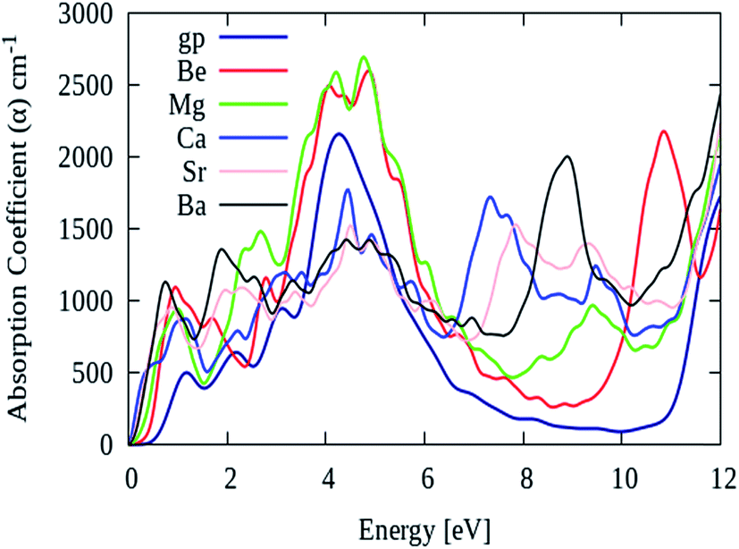 | ||
| Fig. 8 Absorption coefficient of pure graphene (gp) and (Be, Mg, Ca, Sr and Ba) atom-doped graphene. | ||
The reflectivity plots for pure graphene and AEM (Be, Mg, Ca, Sr and Ba) atom-doped graphene structures are shown in Fig. 9(a) and (b), and the comparison is made among all the structural models. The energy interval was set from 0 to 25 eV for calculating reflectivity, in order to determine the overall effect for AEM atom substitution on reflectivity of graphene. In case of pure graphene, there are three main reflectivity peaks with intensity of approximately 0.29, 0.31 and 0.21 at energy levels of 0.7 eV, 4.5 eV and 14 eV, respectively as shown by Fig. 9(a). These results are consistent with previous reports.52,56 However, when AEM atom is substituted into graphene, the reflectivity peaks appearing at 4.5 eV and 14 eV has diminishing peak intensities as the AEM atoms proceed along the group as depicted in Fig. 9(a) and (b), respectively. On the other hand, the first peak with 0.29 intensity at 0.7 eV energy for pure graphene, has increased value of 0.4, 0.41, 0.63, 0.58 and 0.61 for Be, Mg, Ca, Sr and Ba atom substituted monolayer graphene structures as depicted in Fig. 9(a) and (b), respectively. From these results one can summarize that, after AEM atom substitution into graphene, the reflectivity is reduced in the higher energy region and it has increased peak intensity in the low energy region.
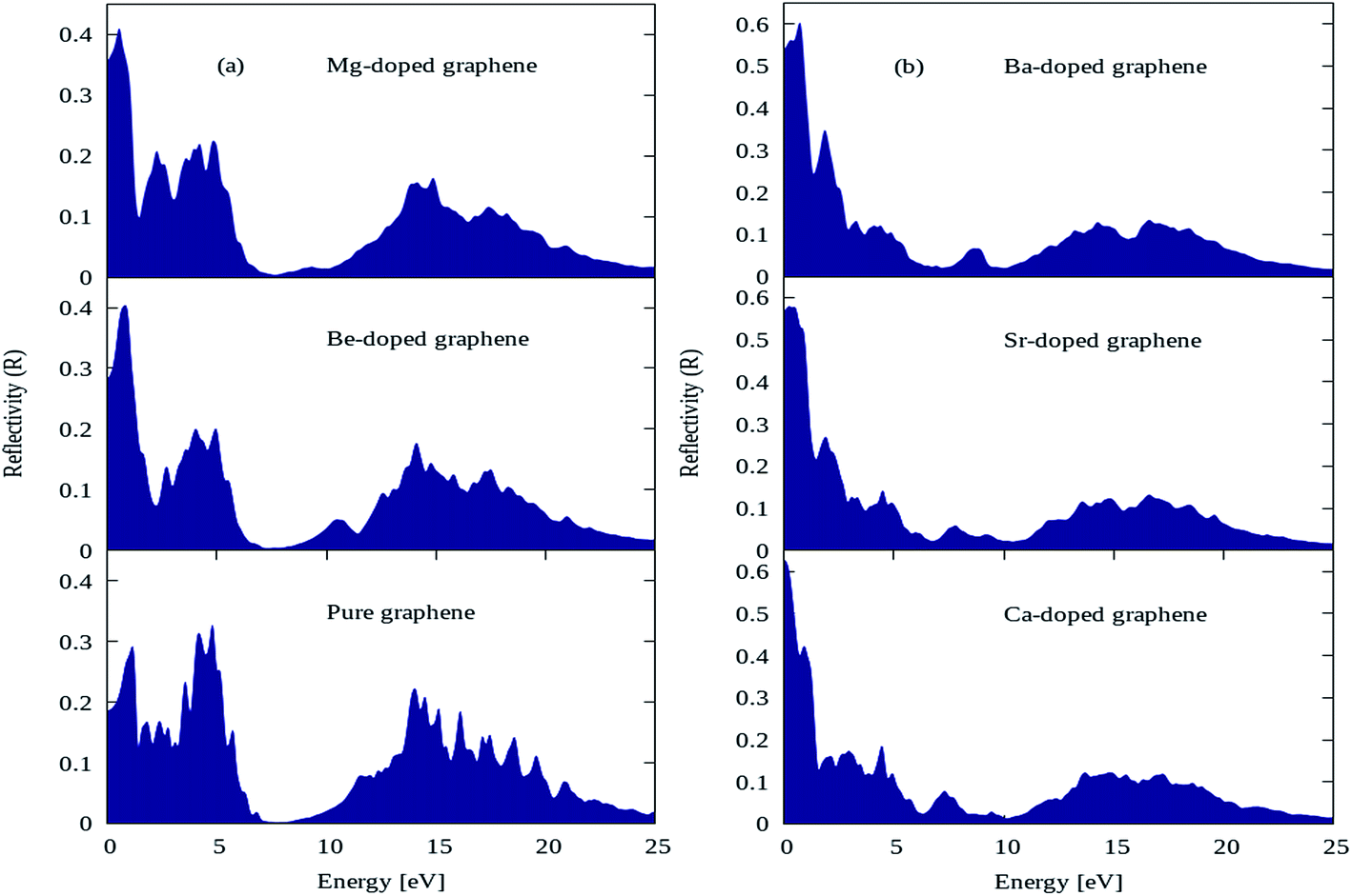 | ||
| Fig. 9 Reflectivity plots for (a) pure, Be, Mg atom-doped and (b) Ca, Sr and Ba atom-doped graphene. | ||
4. Conclusion
In conclusion, we have performed first-principles DFT calculations to investigate the structural, magnetic, electronic and optical properties of alkaline earth metal (AEM) atom-doped monolayer graphene. Different AEM atoms i.e. (Be, Mg, Ca, Sr and Ba) were substituted into 4 × 3 graphene supercell. It was found that all the impurity atoms were tightly bonded with graphene. AEM atom doping into graphene revealed ferromagnetism behavior in monolayer graphene. Obtained total magnetic moments for AEM atom-doped graphene structures were found to be 0.00 μB, 1.86 μB, 4.00 μB, 3.16 μB and 0.46 μB for Be, Mg, Ca, Sr and Ba atom-doped graphene complexes, respectively. Significant ferromagnetic coupling is obtained between impurity AEM atom and neighboring C atoms on the graphene layer. It is intriguing that, AEM atom substitution can modify the electronic and optical properties of graphene. Our calculations for electronic properties reveal that, Be, Mg and Ca atom embedded graphene complexes exhibit half metal behavior, while Sr and Ba atom-doped graphene complexes display indirect band gap semiconductor behavior. It is very important to note here that band gap was sensitively dependent on the nature of dopant atom, which presents a viable approach to tune the gap of monolayer graphene. The calculated PDOS plots reveal that, the sp orbitals of AEM atoms are responsible of arising of magnetic moments in graphene. In addition, PDOS plots also revealed that the, band gaps differed between spin up and spin down state channels. Hence we can predict that, these AEM atom-doped graphene complexes carry potential applications for the development of spintronic devices.The optical absorption and reflectivity plots for all AEM atom-doped graphene structures were also calculated. From the absorption coefficient plots, it was found that pure graphene has two main peaks appearing at 4.8 eV and 14 eV energy levels and it has almost zero absorption between 7–11 eV energy interval. After AEM atom substitution, the maximum absorption coefficient peak present at 14 eV reduces to lower intensity values, and the second minimum peak at 4.8 eV observes a shift in range of 0.1–0.3 eV energy value. Another important modification is obtained in the absorption spectrum of pure graphene, a third minimum peak is obtained in the energy interval of 7–11 eV energy interval after AEM atom substitution, which was not present in the absorption spectrum of pure graphene. From the obtained reflectivity plots, we can summarize that, after AEM atom substitution into graphene, the reflectivity is reduced in the higher energy region and it has increased peak intensity in the low energy region.
We can conclude that, AEM atom substitution in graphene can significantly alter the electronic and magnetic behaviors of graphene, to make it display dilute magnetic semiconductor behavior, thereby making it functional for high speed transistor applications. Similarly, the optical properties of graphene can also be tuned by substituting AEM atoms in monolayer graphene. Our obtained results suggest further experimental investigations in this area, which can lead to the applications of graphene in the fields of photonics and spintronics.
Acknowledgements
This work was supported by the National Natural Science Foundation of China (No. 51522601, 51421063) and the program for New Century Excellent Talents in University (No. NCET-13-0173).References
- K. S. Novoselov, A. K. Geim, S. V. Morozov, D. Jiang, Y. Zhang, S. V. Dubonos, I. V. Grigorieva and A. A. Firsov, Science, 2004, 306, 666–669 CrossRef CAS PubMed.
- K. Novoselov, D. Jiang, F. Schedin, T. Booth, V. Khotkevich, S. Morozov and A. Geim, Proc. Natl. Acad. Sci. U. S. A., 2005, 102, 10451–10453 CrossRef CAS PubMed.
- K. Novoselov, A. K. Geim, S. Morozov, D. Jiang, M. Katsnelson, I. Grigorieva, S. Dubonos and A. Firsov, Nature, 2005, 438, 197–200 CrossRef CAS PubMed.
- L. Ci, L. Song, C. Jin, D. Jariwala, D. Wu, Y. Li, A. Srivastava, Z. Wang, K. Storr and L. Balicas, Nat. Mater., 2010, 9, 430–435 CrossRef CAS PubMed.
- T. Martins, R. Miwa, A. J. Da Silva and A. Fazzio, Phys. Rev. Lett., 2007, 98, 196803 CrossRef CAS PubMed.
- M. Sun, W. Tang, Q. Ren, Y. Zhao, S. Wang, J. Yu, Y. Du and Y. Hao, Phys. E, 2016, 80, 142–148 CrossRef CAS.
- O. V. Yazyev and M. Katsnelson, Phys. Rev. Lett., 2008, 100, 047209 CrossRef PubMed.
- N. Tombros, C. Jozsa, M. Popinciuc, H. T. Jonkman and B. J. Van Wees, Nature, 2007, 448, 571–574 CrossRef CAS PubMed.
- W. Han, K. Pi, K. McCreary, Y. Li, J. J. Wong, A. Swartz and R. Kawakami, Phys. Rev. Lett., 2010, 105, 167202 CrossRef PubMed.
- F. Banhart, J. Kotakoski and A. V. Krasheninnikov, ACS Nano, 2010, 5, 26–41 CrossRef PubMed.
- O. Lehtinen, J. Kotakoski, A. Krasheninnikov, A. Tolvanen, K. Nordlund and J. Keinonen, Phys. Rev. B: Condens. Matter Mater. Phys., 2010, 81, 153401 CrossRef.
- J. Kotakoski, A. Krasheninnikov, U. Kaiser and J. Meyer, Phys. Rev. Lett., 2011, 106, 105505 CrossRef CAS PubMed.
- H. Sahin and F. M. Peeters, Phys. Rev. B: Condens. Matter Mater. Phys., 2013, 87, 085423 CrossRef.
- S. Lisenkov, A. N. Andriotis and M. Menon, Phys. Rev. Lett., 2012, 108, 187208 CrossRef PubMed.
- A. T. Lee, J. Kang, S.-H. Wei, K. Chang and Y.-H. Kim, Phys. Rev. B: Condens. Matter Mater. Phys., 2012, 86, 165403 CrossRef.
- Z. He, K. He, A. W. Robertson, A. I. Kirkland, D. Kim, J. Ihm, E. Yoon, G.-D. Lee and J. H. Warner, Nano Lett., 2014, 14, 3766–3772 CrossRef CAS PubMed.
- K. T. Chan, H. Lee and M. L. Cohen, Phys. Rev. B: Condens. Matter Mater. Phys., 2011, 83, 035405 CrossRef.
- A. Krasheninnikov, P. Lehtinen, A. S. Foster, P. Pyykkö and R. M. Nieminen, Phys. Rev. Lett., 2009, 102, 126807 CrossRef CAS PubMed.
- D. Boukhvalov and M. Katsnelson, Appl. Phys. Lett., 2009, 95, 023109 CrossRef.
- E. J. Santos, A. Ayuela and D. Sánchez-Portal, New J. Phys., 2010, 12, 053012 CrossRef.
- M. Sun, W. Tang, Q. Ren, S. Wang, Y. Du and Y. Zhang, Appl. Surf. Sci., 2015, 356, 668–673 CrossRef CAS.
- M. H. Gass, U. Bangert, A. L. Bleloch, P. Wang, R. R. Nair and A. Geim, Nat. Nanotechnol., 2008, 3, 676–681 CrossRef CAS PubMed.
- C. Casiraghi, A. Hartschuh, E. Lidorikis, H. Qian, H. Harutyunyan, T. Gokus, K. Novoselov and A. Ferrari, Nano Lett., 2007, 7, 2711–2717 CrossRef CAS PubMed.
- P. Blake, E. Hill, A. C. Neto, K. Novoselov, D. Jiang, R. Yang, T. Booth and A. Geim, Appl. Phys. Lett., 2007, 91, 063124 CrossRef.
- G. Eda, Y. Y. Lin, C. Mattevi, H. Yamaguchi, H. A. Chen, I. Chen, C. W. Chen and M. Chhowalla, Adv. Mater., 2010, 22, 505–509 CrossRef CAS PubMed.
- A. Marinopoulos, L. Reining, A. Rubio and V. Olevano, Phys. Rev. B: Condens. Matter Mater. Phys., 2004, 69, 245419 CrossRef.
- O. Sedelnikova, L. Bulusheva and A. Okotrub, J. Chem. Phys., 2011, 134, 244707 CrossRef CAS PubMed.
- T. Eberlein, U. Bangert, R. Nair, R. Jones, M. Gass, A. Bleloch, K. Novoselov, A. Geim and P. Briddon, Phys. Rev. B: Condens. Matter Mater. Phys., 2008, 77, 233406 CrossRef.
- G. Kresse and D. Joubert, Phys. Rev. B: Condens. Matter Mater. Phys., 1999, 59, 1758 CrossRef CAS.
- G. Kresse and J. Furthmüller, Comput. Mater. Sci., 1996, 6, 15–50 CrossRef CAS.
- P. E. Blöchl, Phys. Rev. B: Condens. Matter Mater. Phys., 1994, 50, 17953 CrossRef.
- J. P. Perdew, K. Burke and M. Ernzerhof, Phys. Rev. Lett., 1996, 77, 3865 CrossRef CAS PubMed.
- A. H. Reshak, D. Stys, S. Auluck and I. Kityk, Phys. Chem. Chem. Phys., 2011, 13, 2945–2952 RSC.
- G. Davydyuk, O. Y. Khyzhun, A. Reshak, H. Kamarudin, G. Myronchuk, S. Danylchuk, A. Fedorchuk, L. Piskach, M. Y. Mozolyuk and O. Parasyuk, Phys. Chem. Chem. Phys., 2013, 15, 6965–6972 RSC.
- A. Reshak, Y. Kogut, A. Fedorchuk, O. Zamuruyeva, G. Myronchuk, O. Parasyuk, H. Kamarudin, S. Auluck, K. Plucinski and J. Bila, Phys. Chem. Chem. Phys., 2013, 15, 18979–18986 RSC.
- A. Reshak, Phys. Chem. Chem. Phys., 2014, 16, 10558–10565 RSC.
- A. H. Reshak, RSC Adv., 2014, 4, 39565–39571 RSC.
- A. H. Reshak, RSC Adv., 2014, 4, 63137–63142 RSC.
- M. Rafique, Y. Shuai, H.-P. Tan and H. Muhammad, Appl. Surf. Sci., 2017, 399, 20–31 CrossRef CAS.
- S. Ullah, A. Hussain, W. Syed, M. A. Saqlain, I. Ahmad, O. Leenaerts and A. Karim, RSC Adv., 2015, 5, 55762–55773 RSC.
- J. O. Chapman, Alkali Metal Doped Graphene: Superconductivity, Structural, Magnetic and Optical Properties, University of Manchester, 2015 Search PubMed.
- E. Beheshti, A. Nojeh and P. Servati, Carbon, 2011, 49, 1561–1567 CrossRef CAS.
- A. Ferre-Vilaplana, J. Phys. Chem. C, 2008, 112, 3998–4004 CAS.
- X. Liu, C.-Z. Wang, M. Hupalo, W. Lu, M. C. Tringides, Y. Yao and K.-M. Ho, Phys. Chem. Chem. Phys., 2012, 14, 9157–9166 RSC.
- W. Tang, E. Sanville and G. Henkelman, J. Phys.: Condens. Matter, 2009, 21, 084204 CrossRef CAS PubMed.
- G. Henkelman, A. Arnaldsson and H. Jónsson, Comput. Mater. Sci., 2006, 36, 354–360 CrossRef.
- X. Liu, C.-Z. Wang, M. Hupalo, H.-Q. Lin, K.-M. Ho and M. C. Tringides, Crystals, 2013, 3, 79–111 CrossRef CAS.
- A. K. Geim and K. S. Novoselov, Nat. Mater., 2007, 6, 183–191 CrossRef CAS PubMed.
- F. Guinea, N. Peres, K. Novoselov, A. Geim and A. C. Neto, Rev. Mod. Phys., 2009, 81, 109–162 CrossRef.
- T. Hussain, B. Pathak, T. A. Maark, M. Ramzan and R. Ahuja, Europhys. Lett., 2012, 99, 47004 CrossRef.
- P. Rani and V. Jindal, RSC Adv., 2013, 3, 802–812 RSC.
- R. Muhammad, Y. Shuai and H.-P. Tan, Phys. E, 2017, 88, 115–124 CrossRef CAS.
- M. Wu, C. Cao and J. Z. Jiang, Nanotechnology, 2010, 21, 505202 CrossRef CAS PubMed.
- R. Nascimento, J. d. R. Martins, R. J. Batista and H. Chacham, J. Phys. Chem. C, 2015, 119, 5055–5061 CAS.
- M. Gajdoš, K. Hummer, G. Kresse, J. Furthmüller and F. Bechstedt, Phys. Rev. B: Condens. Matter Mater. Phys., 2006, 73, 045112 CrossRef.
- P. Rani, G. S. Dubey and V. Jindal, Phys. E, 2014, 62, 28–35 CrossRef CAS.
- A. Laref, A. Ahmed, S. Bin-Omran and S. Luo, Carbon, 2015, 81, 179–192 CrossRef CAS.
- C. Shen, C. Tseng, C. Lin, L. Li and H. L. Liu, Thin Solid Films, 2014, 571, 675–679 CrossRef CAS.
- L. Yang, J. Deslippe, C.-H. Park, M. L. Cohen and S. G. Louie, Phys. Rev. Lett., 2009, 103, 186802 CrossRef PubMed.
- F. Nelson, V. Kamineni, T. Zhang, E. Comfort, J. Lee and A. Diebold, Appl. Phys. Lett., 2010, 97, 253110 CrossRef.
| This journal is © The Royal Society of Chemistry 2017 |