
 Open Access Article
 This Open Access Article is licensed under a
 Creative Commons Attribution 3.0 Unported Licence
Deformation and failure mechanisms of electrochemically lithiated silicon thin films
Hansinee Sitinamaluwaa,
Jawahar Nerkara,
Mingchao Wang†
a,
Shanqing Zhangb and
Cheng Yan *a
*a
aSchool of Chemistry, Physics and Mechanical Engineering, Queensland University of Technology (QUT), Brisbane, QLD 4001, Australia. E-mail: c2.yan@qut.edu.au
bCentre for Clean Environment and Energy, Environmental Futures Research Institute and Griffith School of Environment, Gold Coast Campus, Griffith University, QLD 4222, Australia
First published on 28th February 2017
Abstract
A fundamental understanding of mechanical behavior of a Li–Si system is necessary to address the poor mechanical integrity of amorphous silicon (a-Si) electrodes, in order to utilize their enormous capacity in Li-ion batteries. In this work, deformation and failure mechanisms of electrochemically lithiated a-Si thin films were investigated using nanoindentation and molecular dynamics simulation techniques. The cracking observed in the a-Si thin films after the initial lithiation–delithiation cycle is associated with the tension stress developed when constrained by the substrates. The MD simulations provide an atomistic insight on the origin of plasticity and transition of fracture mechanisms with increasing lithium concentration in the electrode. Both experiment and the MD simulations indicate reduced strength, elastic modulus but increased ductility in the a-Si films after the full lithiation–delithiation cycle, as a result of increased disorder in the microstructures. Also, the mapping of void nucleation and growth indicates different failure modes in pristine and delithiated a-Si.
1. Introduction
Li-ion batteries have been applied to a wide range of energy storage devices, ranging from small battery packs for portable electronic devices to large-scale stationary power management and high-power electrical transportation systems. In order to meet increasing demands, further increases in capacity and efficiency of Li-ion batteries are urgently required.1,2 To this end, inorganic electrode materials which store lithium via alloying mechanisms have attracted increasing attention due to their large theoretical capacity.3 For currently used graphite anodes, six carbon atoms can host one lithium atom giving a theoretical capacity of 372 mA h g−1. In contrast, alloying anodes such as Si, Sn, Al, Mg and Bi have much higher lithium storage capacity compared to graphite.4 For example, one silicon atom can bond with 3.75 lithium atoms, having a theoretical capacity of 3579 mA h g−1.5 However, electrochemical lithiation of silicon results in enormous volume expansion (about 300%), high mechanical stress and possible material failure, resulting in early capacity decay.6 Application of nanostructured materials, such as nanoscale thin films, has been confirmed as an effective way to improve the damage tolerance of electrodes.7–10 Several recent studies indicate that amorphous silicon shows increased stability compared to its crystalline counterpart.11,12Thin films are relatively easy to fabricate, but one problem is the mechanical stresses induced by geometrical constraints such as substrates, which may result in large mechanical deformation or failure. Reduction of film thickness may improve the damage tolerance and hence improve the long-term cycling stability.13 To design robust thin film architectures, a fundamental understanding of stresses and mechanical behavior of thin film electrodes is crucially important. Li-induced stress development in silicon thin films has been studied by several researchers.14–16 Also, mechanical behavior of lithiated silicon has been studied previously; Hertzberg et al.17 and Berla et al.18 used nanoindentation to determine the mechanical properties of electrochemically lithiated amorphous silicon (a-Si) thin films. Wafer curvature technique was also used to measure the mechanical performance of lithiated silicon.15,19 Recent ab initio studies have confirmed that the mechanism of lithiation–delithiation is atomistic in nature, which involves breaking and re-forming of covalent Si–Si bonds.20–22 Also, atomistic simulations reveal a brittle-to-ductile transition of amorphous LixSi, due to changes in the phase composition during charge–discharge process.23–25 However, the atomistic mechanisms govern such transition is still unclear. Also, less attention has been paid to understanding the microstructure evolution during the delithiation process, and its effect on the mechanical behavior of delithiated silicon.
To address these issues, we investigated the deformation and failure mechanisms of lithiated a-Si thin films using extensive nanoindentation tests and molecular dynamic simulations. The evolution of morphology and mechanical stresses in an a-Si thin film during charging and discharging cycle and their contributions to the deformation and failure mechanisms are discussed in detail. We believe the outcome of this study can benefit the development of robust electrode architectures with improved mechanical and electrochemical performance.
2. Methods
2.1. Experimental
The a-Si thin films were deposited on polished stainless steel disks. Steel disks were first ground using 1200 grit silicon carbide paper, followed by a Nap-cloth polishing with 1-micron diamond compound. The substrates were thoroughly cleaned by sonicating in ethanol to remove polishing debris. The film deposition was completed using a multi-source RF/DC magnetron sputtering system (Kurt J. Lesker PVD75). We employed a sequential deposition technique for deposition of Ti and Si layers without breaking the vacuum. Initially, a Ti layer (∼25 nm) was deposited from high purity Ti target (99.995% pure) by DC sputtering at 100 W and 10 mTorr. Next, amorphous silicon thin film was deposited by RF magnetron sputtering at 60 W and 4 mTorr using undoped silicon target. The substrate holder was allowed to rotate at 20 rpm to keep the uniformity of the films. Prior to the film deposition, a pre-sputtering of 5 min was allowed to remove any surface contamination from the source target and also to stabilize the sputtering conditions. The deposition process was carried out at room temperature.Surface morphology of thin films was characterized by Scanning Electron Microscopy (SEM) at 5 kV acceleration voltage. Raman measurements were carried out using Renishaw Raman microprobe with 633 nm laser source. For the electrochemical tests, coin cells (CR2032) were assembled using the sputtered silicon films as the working electrode, a Li foil as the counter electrode and a 25 μm thick 2325 Celgard separator membrane (Polypore Company). Electrolyte used is 1.0 M LiPF6 in EC/DEC = 50/50 (v/v) (Selectilyte G1, BASF Corporation). Electrochemical tests were carried out using a Bio-Logic VMP-300 electrochemical galvanostat/potentiostat. Galvanostatic charge–discharge tests were performed at a constant current of 0.2 μA (C/10 rate). Lithiation was performed until the cell is discharged to 10 mV vs. Li/Li+, and delithiation was performed by charging the cell to 1.5 V vs. Li/Li+.
For nanoindentation test, thin films with partially and fully lithiated states were prepared by controlling the cell discharge voltage. To prepare fully lithiated thin films, the cells were first discharged to 0.01 V and held at that voltage for additional six hours to complete the lithiation reaction. For the partially lithiated films, the discharge process was terminated at desired voltage level and the cell was allowed to relax at open circuit state for additional six hours. After electrochemical tests, Si/Li cells were disassembled inside a glove box (H2O: <0.1 ppm; O2: <0.1 ppm) running under an inert atmosphere of high purity Ar gas. Cycled Si electrodes were carefully extracted from the opened cells, followed by quickly rinsing with dimethyl carbonate to remove any residual lithium salt. For SEM analysis, electrodes were mounted on SEM stubs inside the glove box and transferred in sealed vials, and were loaded into SEM chamber and pumped down within 30 s to minimize oxidation. The lithiated thin films used for mechanical testing were immersed in paraffin oil inside the glove box, prior to transferring to the nanoindenter.
2.2. Molecular dynamic simulation
Lithiation–delithiation process of amorphous silicon (a-Si) was investigated using molecular dynamics (MD) simulations. Melt-and-quench scheme was first adopted to create the initial amorphous silicon structure with the dimensions of 5 × 5 × 5 nm3.26 To simulate the lithiation stage, a small amount of lithium was initially distributed in the a-Si cell and the system was fully relaxed in the NPT ensemble at 300 K for 10 ps. This procedure was repeated until the desired Li concentration was reached. To simulate the delithiation stage, a small number of randomly-selected Li atoms were removed from the structure, and the system relaxation was carried out in the NPT ensemble at 300 K for 10 ps. For the calculation of Li-induced stress, the cubic a-Si atomic model of side length 5 nm is considered as a small volume element in a geometrically constrained thin film. During the simulation of lithiation–delithiation, expansion of the cubic a-Si unit is restricted in the x–y plane (parallel to the substrate plane) but the Li-induced volume expansion is possible along the z direction (normal to the substrate plane). The bi-axial stress along the x–y plane during lithium insertion/extraction is calculated using the virial theorem.27,28 The detailed simulation method is reported elsewhere.29For the uniaxial tension test, cubic models of 5 × 5 × 5 nm3 were cut out from the lithiated structures followed by equilibration in the NPT ensemble at 300 K for 10 ps. Following the equilibration, the uniaxial tension test was carried out in the simulation cell in z-direction at a constant strain rate of 5 × 10⁸ s−1. Similarly, the triaxial tension test was conducted via displacement in all three directions at a constant strain rate of 5 × 10⁸ s−1. The virial theorem was used to calculate the atomic stresses during tensile deformation.27,28 Cavitation (i.e. void nucleation and coalescence) in the a-Si cell under the hydrostatic stress was analyzed using the Mercury30 software. All simulations were performed using the Large-scale Atomic/Molecular Massively Parallel Simulator (LAMMPS).31 Atomic interactions of a-Si and Li–Si systems were described using modified Stillinger–Weber potential,32 and MEAM-based interatomic potential,33 respectively.
3. Results and discussion
3.1. Characterization of thin films
Fig. 1a and b show the SEM images of as-deposited a-Si thin film, i.e., the cross-section and the surface, respectively. The a-Si layer is quite smooth and uniform with a thickness of ∼200 nm. Small blisters can be observed on the surface, as indicated by the arrows in Fig. 1b. Sputter deposition of Si at room temperature results in an amorphous structure, as confirmed by Raman spectrum, Fig. 1c. The Raman peaks assigned to a-Si vibration modes are clearly visible at 155 cm−1 (transverse acoustic – TA), 310 cm−1 (longitudinal acoustic – LA), 400 cm−1 (transverse optic – TO) and 475 cm−1 (longitudinal optic – LO).34 Also, the Raman peak around 630 cm−1 corresponds to the 2LA second-order phonon and TO + TA overtone.34 Fig. 1d shows the initial galvanostatic charge–discharge profiles (between 0.01 and 1.5 V at C/10 rate) of an electrochemical cell built with a-Si thin film working-electrode vs. metallic lithium counter-electrode. The discharge/charge curve is in agreement with previous electrochemical data reported for a-Si electrodes.18,35,36 The a-Si film has the discharge capacity of 3378 mA h g−1 and charge capacity of 2702 mA h g−1, resulting in 80% coulombic efficiency during the initial cycle.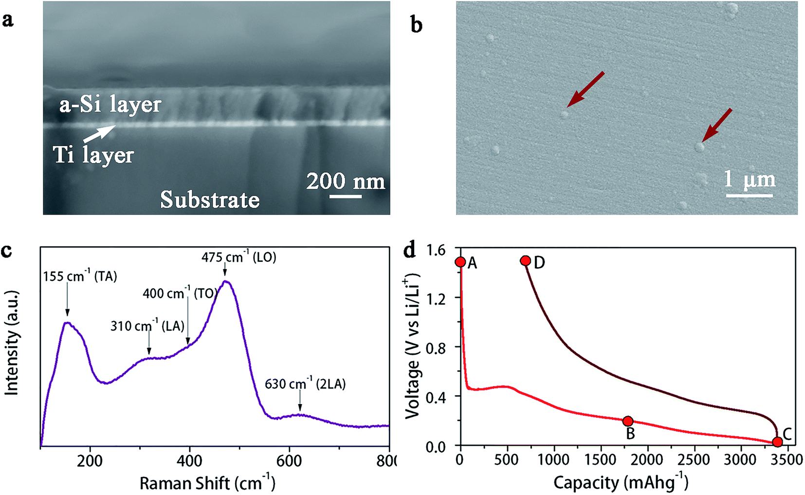 | ||
| Fig. 1 (a) SEM cross-section image and (b) surface morphology of a-Si thin film, (c) Raman spectrum analysis and (d) first-cycle galvanostatic charge–discharge curves of the a-Si thin film electrode. | ||
In Fig. 2, SEM images indicate the surface morphology of the a-Si thin film during the initial lithiation and delithiation cycle. The pristine film consists of clusters of small spherical particles (Fig. 2b), a typical feature of sputtered thin films.37 Upon lithiation, the Li–Si alloying reaction leads to a volume expansion of the film, up to 300%.11 Large blisters appear in the fully lithiated thin film (Fig. 2c), apparently due to the volume expansion of those blisters observed in pristine a-Si surface (Fig. 1b). As the expansion of the film is restricted by the substrate, mechanical stress is generally expected.6 However, there are no observable cracks in the fully lithiated films. Removal of lithium upon delithiation results in the formation of cracks (>10 μm) after the first delithiation as shown in Fig. 2e. Also, the morphology is changed after the first delithiation as observed in Fig. 2f.
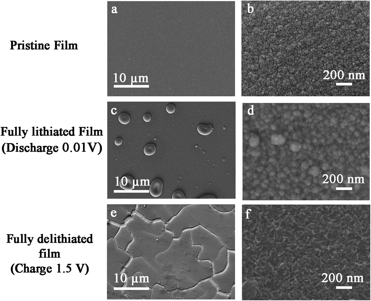 | ||
| Fig. 2 SEM micrographs of surface morphology evolution during lithiation–delithiation cycle. (a and b) Pristine film, (c and d) fully-lithiated film and (e and f) fully-delithiated film. | ||
3.2. Structure and properties of lithiated a-Si thin films
Thin films at several lithiation/delithiation states (indicated by A, B, C and D in Fig. 1d) were prepared for the nanoindentation test. These states correspond to (A) pristine a-Si, (B) Li1.8Si, (C) Li3.75Si and (D) delithiated a-Si. Due to the reactivity of lithium containing films, they were fully immersed in a paraffin oil bath during the nanoindentation test. To understand possible influence of paraffin oil on the indentation test, several reference materials were firstly tested in both air and the oil and no notable difference was observed. Fig. 3 shows indentation load–displacement curves for the thin films under ∼1 mN maximum load. The observed load–displacement responses are clearly different depending on the charge–discharge state of the films. The energy dissipated during loading is manifested as both elastic and plastic deformation, which is partially recovered in an elastic manner during unloading.38 The total energy dissipated is represented by the area enclosed within the loading–unloading curves. From Fig. 3, the energy dissipated during indentation process is calculated as 1.39 × 10⁻¹¹ J, 3.79 × 10⁻¹¹ J, 4.70 × 10⁻¹¹ J and 2.51 × 10⁻¹¹ J for pristine a-Si, Li1.8Si, Li3.75Si and delithiated a-Si respectively. It is clear that the amount of energy dissipated increases with increasing lithium concentration. Neglecting residual elastic strain, such difference can be attributed to large plastic deformation of the lithiated films. Interestingly, the delithiated a-Si film exhibits increased plasticity compared to pristine a-Si, indicating that the original a-Si structure cannot be recovered after delithiation.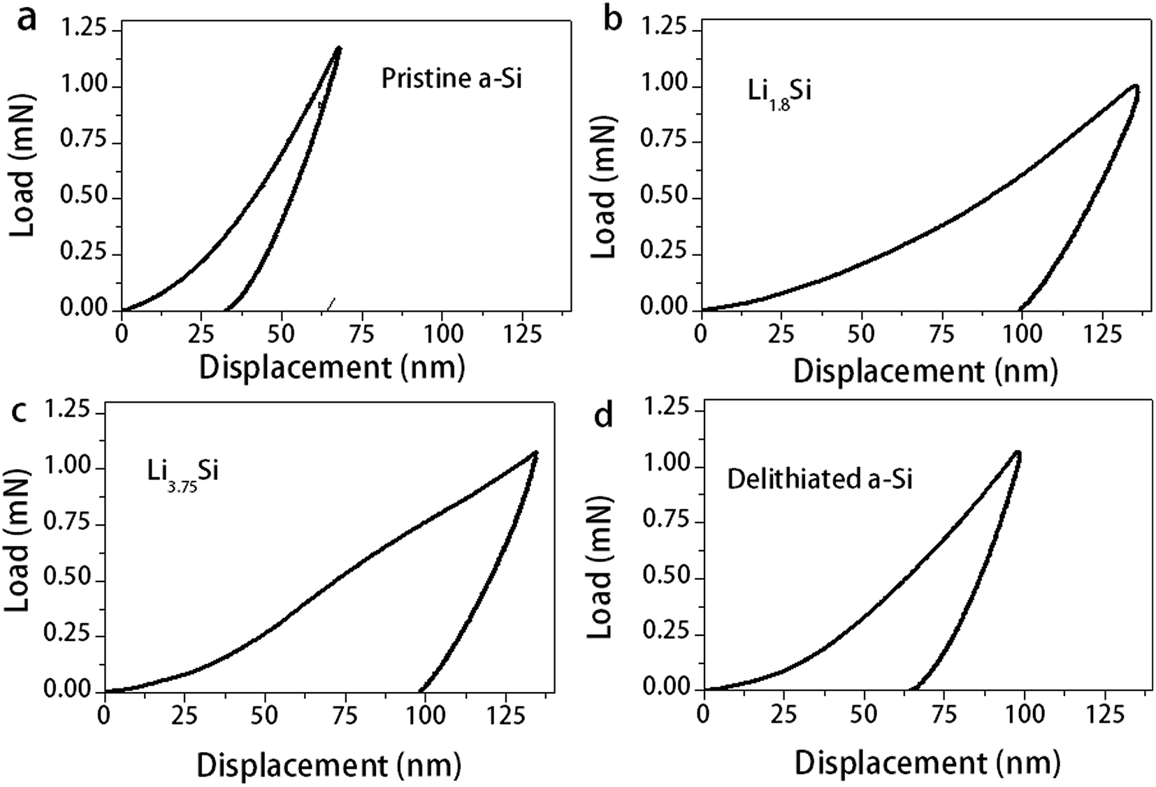 | ||
| Fig. 3 Nanoindentation load–displacement curves for (a) pristine a-Si (b) Li1.8Si (c) Li3.75Si and (d) delithiated a-Si films. | ||
Also, the strong stress-potential coupling (100–120 mV GPa−1)39 in the lithiated a-Si thin film can result in non-uniform concentration gradients in and around the indentation volume. Considering the Li diffusion coefficient (D) in a-Si thin film (in the order of 2 × 10⁻⁹ cm2 s−1),40,41 the time scale for Li ions to diffuse through a-Si thin film (thickness L of ∼200 nm) is in the order of 0.2 s (t ∼ L2/D), which is smaller than the relaxation time (2 s) during nanoindentation. It is thus sufficient for Li diffusion to dissipate the indentation-induced lithium concentration gradients. Therefore, and the LixSi film can be considered as a homogeneous material, where the conventional approach of Oliver and Pharr is appropriate for the analysis of nanoindentation load–displacement data.
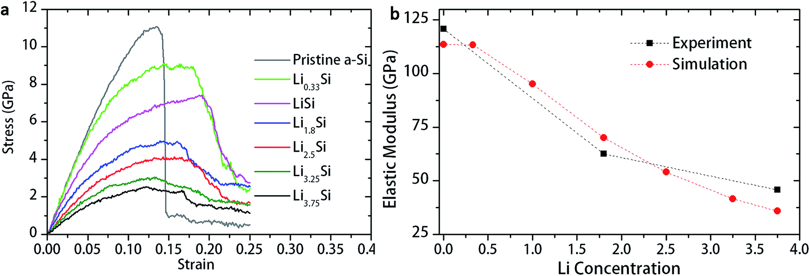
The elastic modulus and hardness of the thin films were estimated using partial unloading method to remove possible substrate effect. Ten indentations were conducted for each sample, and the modulus and hardness for each unloading section were analyzed using Oliver and Pharr method.42 The average reduced modulus vs. contact depth was extrapolated to zero contact depth to obtain the true reduced modulus.38 Table 1 summarizes the elastic modulus and hardness of the thin films. Progressive softening of LixSi with increasing Li concentration can be observed, with a drop of elastic modulus from 120 GPa to 45.7 GPa and a hardness drop form 9.9 GPa to 1.9 GPa after full lithiation. The progressive softening of a-Si thin films are in good agreement with the initial first-principle studies reported by Shenoy et al.,43 where the young's modulus of a-Si and Li15Si4 was reported as ∼95 GPa and ∼40 GPa respectively. Also, these first principle studies show a linear decrease in these properties with increasing Li concentration. However, the nanoindentation results reported here show that the elastic modulus and hardness decrease with Li concentration in a nonlinear manner. At 50% full capacity of Li insertion, 48% reduction in elastic modulus and 76% reduction in hardness can be observed. Corresponding to full lithiation, however, further reduction in elastic modulus and hardness is only 13% and 4%, respectively. As identified in our previous molecular dynamic simulations,29 the initial breakdown of Si–Si bonds takes place up to the formation of Li2.5Si, followed by relatively slower bond breaking to form Li3.75Si. We believe these structural changes are responsible for the evolution of elastic modulus and hardness observed. Furthermore, the elastic modulus and hardness are not fully recovered after removal of lithium, as the delithiated a-Si film shows reduced elastic modulus from 120 GPa to 80 GPa, and a drop of hardness from 9.9 GPa to 3.5 GPa. To unveil the responsible atomistic mechanisms, we conducted extensive MD simulations to investigate the evolution of LixSi atomic structures, mechanical stress and failure during lithiation–delithiation cycles.
| Lithiation/delithiation state | Composition | Elastic modulus (GPa) | Hardness (GPa) |
|---|---|---|---|
| A – pristine | 100% Si | 120.8 | 9.9 |
| B – partially (∼50%) lithiated (0.2 V discharge) | Li∼1.8Si | 62.5 | 2.3 |
| C – fully lithiated (0.01 V discharge) | Li∼3.75Si | 45.7 | 1.9 |
| D – fully delithiated (1.5 V charge) | ∼100% Si | 80.0 | 3.5 |
The possible reason for crack formation in the thin films (Fig. 2e) is the in-plane stresses caused by volume expansion and geometrical constraint by the substrate.14,19,44 The in-plane bi-axial stresses in a constrained a-Si thin film during lithiation–delithiation cycle can be modeled using MD routine as shown in Fig. 4. The Li concentration in the simulations (x in LixSi) ranges from 0 to 3.75, which corresponds to the Li intake observed at room temperature (formation of Li15Si4, at a capacity of 3579 mA h g−1).45 As shown in Fig. 4, compressive stress is developed during lithiation. Corresponding to lower Li concentrations (x < 0.25), there is a sharp increase of compressive stress. Then, gradual stress relaxation is observed with the increase of Li concentration. On the other hand, the stress is changed to tension during delithiation with a sharp rise at the final stage (x < 0.5). The residual stress is about 2 GPa at the end of the cycle (x = 0). The sharp rise of tensile stress is believed to be the reason for cracking observed during the final stage of the delithiation. Also, the observed stress variations during lithiation–delithiation are considered to be associated with the change of the microstructure and mechanical properties. At low Li concentrations, large stresses can be built up as the structure is dominated by covalent Si–Si bonds. Instead, at a higher Li concentration, lithium rich phases can flow plastically to accommodate volume expansion. Thus, high Li concentration results in reduced mechanical stress, due to increased proportion of Li–Li bonds.
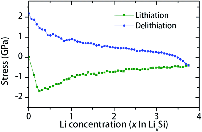 | ||
| Fig. 4 MD simulation of in-plane stress in the a-Si thin film constrained by a substrate during the initial lithiation–delithiation cycle. | ||
It is well known that the lithiation reaction in silicon progresses via separation of covalent Si–Si bonds and creating new Si–Li and Li–Li bonds, to form LixSi intermetallic phases.22,46 Obviously, the microstructural changes of these phases are responsible for their macroscopic mechanical properties. For the a-Si and LixSi amorphous phases, we conducted the Voronoi analysis which can be used to characterize the short range order of these structures. Also, we systematically investigate the evolution of atomic packing with increasing Li concentration and the deformation–failure process under uniaxial tension. In the Voronoi analysis, space is subdivided into a set of convex polyhedra called Voronoi cells, based on a set of points which define the center of each atom.47 For each atom, there is a corresponding polyhedron consisting of all points closer to that atom than to any other. In general, a Voronoi cell represents the volume region occupied by the corresponding atom, thus it is a good indication of atomic packing in the space.
Fig. 5a shows the range of Voronoi cell volume observed for a-Si and LixSi structures for several lithium concentration (x) values spanning from 0 to 3.75. Firstly, amorphous silicon (x = 0), shows much larger Voronoi volume range of 20.7 ± 1.1 Å3. This is because the a-Si structure forms a network of tetrahedrally bonded atoms, which consist of large interstitial spaces (Fig. 5b). These spaces are referred as Td-like positions, which act as favourable sites for Li insertion.20,21 With Li atoms filling into interstitial spaces, the Voronoi volume of silicon atoms tends to decrease, as shown in Fig. 5a. With the Si–Si bond breaking and Si–Li bond formation, the structure becomes more closely packed as x reaches 1.8. Fig. 5c and d shows local atomic structures of Li0.33Si and Li1.8Si respectively.
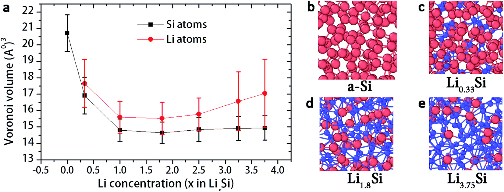 | ||
| Fig. 5 (a) Evolution of Voronoi volume of atoms with increasing Li concentration (b) local atomic structure of a-Si, (c) Li0.33Si (d) Li1.8Si and (e) Li3.75Si. Blue spheres represent Li atoms and red spheres represent Li atoms. | ||
In our previous work,29 we showed that the breakdown of Si–Si bonds dominantly takes place up to formation of Li2.5Si. At Li2.5Si, the silicon atoms are formed into isolated Si anions, Si–Si dumbbells and small clusters consisting with few Si atoms. When x >2.5, more lithium ions invaded to the structure to create more Li-rich regions. Local atomic structures suggest that the Li atoms tend to cluster together in these high Li concentrations (Fig. 5e). Wan et al. showed that the negatively charged zones created by broken Si–Si bonds act as the main driving force for Li atom clustering.48 Also, from Fig. 5a, it can be observed that the Voronoi volume of Li atoms is gradually increasing when x >2.5, while the Voronoi volume of Si atoms remains stable. We believe that these Li rich atomic clusters create more loosely packed regions, resulting in increase of Voronoi volume of Li atoms when x >2.5. Also, these Li-rich atomic clusters are believed to be responsible for extensive plastic deformation.
To further understand the deformation mechanisms and its dependence on microstructures, uniaxial tension was conducted in LixSi structures (x = 0, 1, 1.8, 2.5, 3.25 and 3.75) using molecular dynamic simulation. The simulated stress–strain curves are shown in Fig. 6a. The stress–strain curve for pristine a-Si shows almost linear response similar to brittle materials. The LixSi structures, in contrast, demonstrate an initial linear response followed by significant plastic deformation. Increase of lithium concentration decreases strength of LixSi, but increases the ductility. The estimated elastic moduli are in good agreement with experimental measurement, as shown in Fig. 6b.
 | ||
| Fig. 6 (a) Stress–strain behavior of LixSi structures under uniaxial tension, and (b) elastic modulus of LixSi evaluated by nanoindentation and MD simulation. | ||
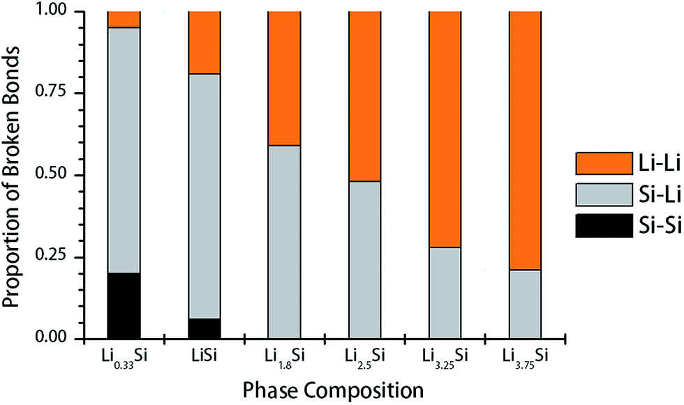
To understand the mechanisms underpinning progressive softening and extensive plasticity, the change of Si–Si, Si–Li and Li–Li bonds during tensile test was examined. Firstly, the radial distribution function (RDF) of undeformed structures was evaluated to determine the cutoff distances for each pair. Considering the first minima of corresponding RDF, the Si–Si cutoff distance is calculated as 3.0 Å, while both Li–Si and Li–Li cutoff distances are evaluated as 3.5 Å. To study the bond breaking, we first counted the number of each type of bonds present in the undeformed structures, and also in the deformed structures after reaching total strain of 0.25. Next, the proportion of each type of bonds to the total number of broken bonds was calculated for each lithium concentration. The proportion of Si–Si, Si–Li and Li–Li bonds participated in fracture in Li–Si phases are shown in Fig. 7. It should be noted that the Si–Si, Li–Si and Li–Li bonds inherit different characteristics. The covalent Si–Si bonds are generally strong, highly directional and resistant to plastic deformation. On the other hand, Si–Li bonds show a weak ionic–covalent character and able to accommodate some plastic deformation.25 The Li–Li bonds are metallic in nature, which are non-directional bonds and having highest degree of freedom to rearrange under load. In Fig. 7, for structures with lower Li concentrations (Li0.33Si, LiSi), the fracture predominantly occurs by breaking of Si–Li and Si–Si bonds, thereby exhibiting relatively high strength, but limited plastic deformation. As the Li concentration increases, Si–Si bonds no longer participate in the deformation. Instead, Li–Li bonds starts to dominate the deformation and final fracture, especially when x >2.5 or higher.
 | ||
| Fig. 7 Contribution of each type of bonds for failure of LixSi structures under uniaxial tension. | ||
Fig. 8 further elucidates the bond breaking mechanisms of Li0.33Si, Li1.8Si and Li3.75Si phases during tensile deformation. For Li0.33Si structure given in Fig. 8a, it is clear that the fracture is dominated by breaking of Si–Li bonds. This is obvious as the Si–Li bonds are of lower strength than Si–Si bonds. It can be observed that the Si–Si bonds still hold the structure together even after the failure of Si–Li bonds (Fig. 8a right panel). Fig. 8b shows the fracture process of Li1.8Si. In this structure, both Si–Li and Li–Li bonds equally participate at the fracture process. In Li3.75Si structure, the clustering of Li atoms is observed, as marked in Fig. 8c (left panel). Also, in Fig. 8c, we observed that failure predominantly occurs in these Li rich regions. We believe that Li–Li bonds are weaker than Si–Si and Si–Li bonds; hence the fracture predominantly occurs at these Li rich atomic clusters.
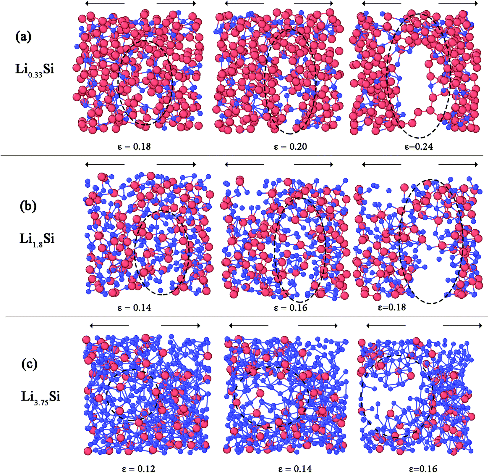 | ||
| Fig. 8 Fracture mechanisms of (a) Li0.33Si (b) Li1.8Si and (c) Li3.75Si structures. Blue spheres represent Li atoms and red spheres represent Si atoms. The symbol ε represents the strain level. | ||
3.3. Deformation and fracture mechanisms of delithiated a-Si
In Table 1, large drop of elastic modulus (from 120 to 80 GPa) and hardness (from 9.9 to 3.5 GPa) can be observed for the fully delithiated a-Si. In other words, the material has started to become softer or plastic after subjecting to a complete lithiation–delithiation cycle. To reveal the responsible atomistic details, we performed MD simulations to investigate the structure–property relationship of the material before and after lithiation–delithiation process. Firstly, the pristine a-Si and delithiation a-Si structures were subjected to triaxial tensile stress by deforming the simulation cell in all three directions at a constant strain rate of 108 s−1. Fig. 9 shows the triaxial stress in the a-Si structures as a function of volumetric strain (εv). The pristine a-Si and delithiated a-Si structures show notable differences in stress–strain behavior. Firstly, the pristine a-Si shows a larger peak stress of 9.64 GPa, compared to that of delithiated a-Si (7.19 GPa). Secondly, pristine a-Si shows catastrophic failure similar to brittle materials, while the delithiated structure undergoes some plastic deformation during fracture. The increased plasticity of delithiated a-Si was also observed in nanoindentation test, as described in Section 3.2.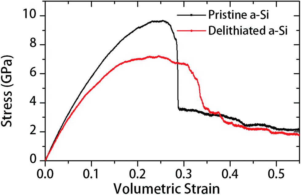 | ||
| Fig. 9 Triaxial tension stress with respect to volumetric strain for pristine and delithiated a-Si structures. | ||
It is anticipated that the lithiation-induced microstructural changes are responsible for the changed mechanical behavior of delithiated a-Si. To understand the microstructural changes, the coordination number before and after the first lithiation–delithiation cycle was evaluated as shown in Fig. 10a. Amorphous silicon has a disordered tetrahedral structure,49 and defect-free a-Si has a coordination number (CN) of 4. Therefore, the coordination analysis (Fig. 10a) shows that there is an increase of over-coordinated (CN = 5, 6) and under-coordinated (CN = 3) atoms in the delithiated a-Si. Furthermore, the radial distribution functions (RDF) of the two structures are evaluated and compared in Fig. 10b. The RDF of the pristine a-Si is in good agreement with experimental results of Laaziri et al.,49 with the first neighbor peak at 2.6 Å. However, after initial lithiation–delithiation cycle the first neighbor peak is shifted to a larger pair distance, which is an indication of weakened Si–Si bonds.46
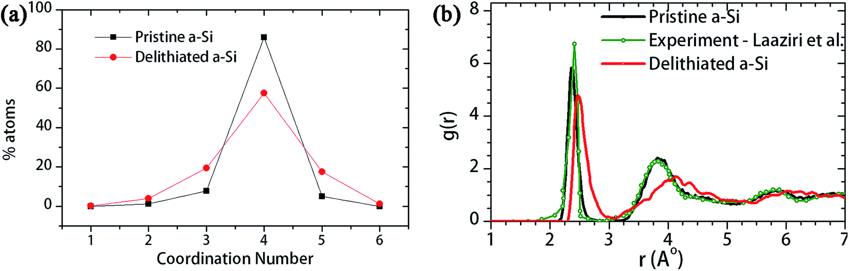 | ||
| Fig. 10 (a) Coordination number and (b) radial distribution function (RDF) of the pristine a-Si and a-Si after first lithiation–delithiation cycle. | ||
Demkowicz and Argon50 presented a theory of plasticity in amorphous silicon, where the dense-liquid like atomic environments act as plasticity carriers. To identify the plasticity carriers in a-Si, Demkowicz and Argon presented a measure of local atomic configurations, which can be evaluated through the bond angles of each atom with nearest neighbors. Every atom i in the structure have mi nearest neighbor atoms within the cutoff distance, and these bonds define x nearest neighbor bond angles for atom i. For example, a four coordinated atoms has six bond angles with its nearest neighbors. The solid diamond-like configurations show mean bond angle close to 109°, with smaller standard deviation. On the other hand, the dense ‘liquid-like’ configurations show relatively smaller mean bond angle with larger standard deviation. To identify the ‘solid-like’ and ‘liquid-like’ configurations, the distribution of mean and standard deviation of bond angles for pristine and delithiated structures are plotted in Fig. 11a and b respectively. According to Fig. 11a, the four-coordinated atoms show the ‘solid-like’ configurations with bond angles closer to 109°. There are a small number of over-coordinated atoms, which show ‘liquid-like’ atomic arrangement. The delithiated a-Si model has same number of atoms, but amount of 4-coordinated atoms are decreased and the over-coordinated and under-coordinated atoms are increased. According to Fig. 11b, the amount of ‘liquid like’ atoms in delithiated a-Si is increased with the increase of over-coordinated atoms. Thus, the bond angle analysis suggests that delithiated a-Si structure have increased number of plasticity carriers compared to pristine a-Si. Also, Fig. 11 shows the increase of under-coordinated (CN = 3) atoms, which creates low density regions in the structure. These regions often act as void nucleation sites during fracture process.23 The analysis of cavitation (i.e. void nucleation and growth) of these structures during triaxial tension is presented in Fig. 12.
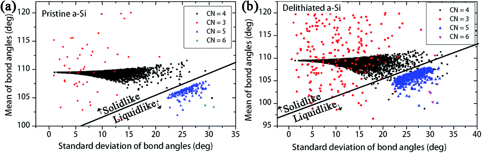 | ||
| Fig. 11 Local atomic environment in (a) pristine a-Si and (b) delithiated a-Si, separated into two distinct types according to the means and standard deviations of bond angles with nearest neighbor atoms. | ||
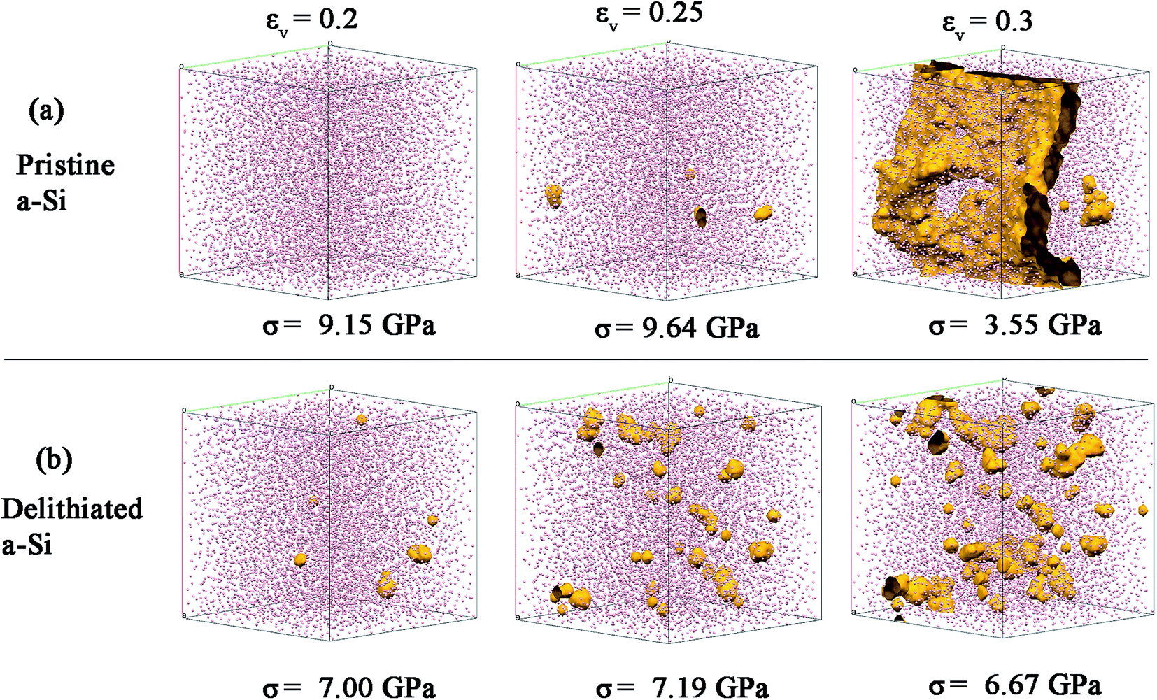 | ||
| Fig. 12 Void nucleation and growth in (a) pristine and (b) delithiated a-Si structures. | ||
The cavitation process (nucleation and growth of voids) due to bond breaking was mapped using a spherical probe with the diameter of 3 Å, which can be swept through the voids or channels in the structure. In Fig. 12, the evolution of the voids with volumetric strain (0.2, 0.25 and 0.3) is shown. There are relatively fewer sites for void nucleation for pristine a-Si (Fig. 12a). These voids link quickly with increase of strain (0.3), leading to the final failure. This is similar to typical brittle fracture in solids at which catastrophic fracture initiates from structure defects such as voids. On the other hand, delithiated a-Si shows a large number of void nucleation sites due to increased number of under-coordinated atoms (Fig. 12b). Also, voids gradually increase and coalescence with the increasing strain, demonstrating a feature often observed in ductile fracture. The ductile behavior may be also related to the increase of dense ‘liquid like’ configurations. Therefore, the atomic disorder induced by lithiation–delithiation process results in cavitation of a-Si at lower stress, but also result in increased ductility during fracture.
4. Conclusions
In this work, the structure, mechanical properties and deformation and failure mechanism of amorphous silicon thin film electrodes has been studied using nanoindentation and molecular dynamic simulations. Cracking has been observed in these 200 nm a-Si thin film after initial lithiation–delithiation cycle. The stress analysis of the a-Si films constrained by substrate indicates that a high tension stress (2 GPa) is generated upon full delithiation, which contributes to the cracking observed. Both experiment and the MD simulations confirm reduced strength, elastic modulus but increased ductility in these a-Si films after the lithiation–delithiation cycle. The MD simulations reveal the transition of fracture mechanisms of LixSi around x ∼2.5. When x <2.5, fracture is dominated by breaking of Li–Si bonds; but the breaking of metallic Li–Li bonds start to dominate the fracture when x >2.5. As the Li concentration increases, the increased number of Li–Li bonds create more loosely packed atomic environment, which facilitates the extensive plastic deformation of the material. After one cycle, increased disorder has been observed in the delithiated a-Si with over-coordinated and under-coordinated atoms. The mapping of void nucleation and growth indicates different failure modes in pristine and delithiated a-Si, i.e., brittle and ductile fracture, respectively. We believe these results contribute to a better understanding of the deformation and failure of lithiated Si.Acknowledgements
The authors wish to acknowledge the Central Analytical Research Facility (CARF) and High Performance Computing (HPC) Service of Queensland University of Technology. HS would like to acknowledge Queensland University of Technology for financial support given by APA, IPRS and QUT excellence top up scholarships. Also, authors wish to acknowledge the financial support from an ARC Discovery Project (DP150101717).References
- L. Lu, X. Han, J. Li, J. Hua and M. Ouyang, J. Power Sources, 2013, 226, 272–288 CrossRef CAS.
- M. M. Thackeray, C. Wolverton and E. D. Isaacs, Energy Environ. Sci., 2012, 5, 7854–7863 CAS.
- W.-J. Zhang, J. Power Sources, 2011, 196, 13–24 CrossRef CAS.
- L. Croguennec and M. R. Palacin, J. Am. Chem. Soc., 2015, 137, 3140–3156 CrossRef CAS PubMed.
- M. T. McDowell, S. W. Lee, W. D. Nix and Y. Cui, Adv. Mater., 2013, 25, 4966–4985 CrossRef CAS PubMed.
- A. Mukhopadhyay and B. W. Sheldon, Prog. Mater. Sci., 2014, 63, 58–116 CrossRef CAS.
- M. Ko, S. Chae, S. Jeong, P. Oh and J. Cho, ACS Nano, 2014, 8, 8591–8599 CrossRef CAS PubMed.
- N. Liu, Z. Lu, J. Zhao, M. T. McDowell, H.-W. Lee, W. Zhao and Y. Cui, Nat. Nanotechnol., 2014, 9, 187–192 CrossRef CAS PubMed.
- H. Sitinamaluwa, S. Zhang, W. Senadeera, G. Will and C. Yan, Mater. Tech., 2016, 31, 872–883 CrossRef CAS.
- M. Ge, X. Fang, J. Rong and C. Zhou, Nanotechnology, 2013, 24, 422001 CrossRef CAS PubMed.
- M. T. McDowell, S. W. Lee, J. T. Harris, B. A. Korgel, C. Wang, W. D. Nix and Y. Cui, Nano Lett., 2013, 13, 758–764 CrossRef CAS PubMed.
- L. A. Berla, S. W. Lee, I. Ryu, Y. Cui and W. D. Nix, J. Power Sources, 2014, 258, 253–259 CrossRef CAS.
- T. Takamura, S. Ohara, M. Uehara, J. Suzuki and K. Sekine, J. Power Sources, 2004, 129, 96–100 CrossRef CAS.
- V. A. Sethuraman, M. J. Chon, M. Shimshak, V. Srinivasan and P. R. Guduru, J. Power Sources, 2010, 195, 5062–5066 CrossRef CAS.
- M. J. Chon, V. A. Sethuraman, A. McCormick, V. Srinivasan and P. R. Guduru, Phys. Rev. Lett., 2011, 107, 045503 CrossRef CAS PubMed.
- M. Pharr, Z. Suo and J. J. Vlassak, J. Power Sources, 2014, 270, 569–575 CrossRef CAS.
- B. Hertzberg, J. Benson and G. Yushin, Electrochem. Commun., 2011, 13, 818–821 CrossRef CAS.
- L. A. Berla, S. W. Lee, Y. Cui and W. D. Nix, J. Power Sources, 2015, 273, 41–51 CrossRef CAS.
- V. A. Sethuraman, M. J. Chon, M. Shimshak, N. Van Winkle and P. R. Guduru, Electrochem. Commun., 2010, 12, 1614–1617 CrossRef CAS.
- G. A. Tritsaris, K. Zhao, O. U. Okeke and E. Kaxiras, J. Phys. Chem. C, 2012, 116, 22212–22216 CAS.
- S. Huang and T. Zhu, J. Power Sources, 2011, 196, 3664–3668 CrossRef CAS.
- E. D. Cubuk and E. Kaxiras, Nano Lett., 2014, 14, 4065–4070 CrossRef CAS PubMed.
- B. Ding, X. Li, X. Zhang, H. Wu, Z. Xu and H. Gao, Nano Energy, 2015, 18, 89–96 CrossRef CAS.
- H. Wang and H. B. Chew, Extreme Mechanics Letters, 2016, 9, 503–513 CrossRef.
- K. Zhao, W. L. Wang, J. Gregoire, M. Pharr, Z. Suo, J. J. Vlassak and E. Kaxiras, Nano Lett., 2011, 11, 2962–2967 CrossRef CAS PubMed.
- A. France-Lanord, E. Blandre, T. Albaret, S. Merabia, D. Lacroix and K. Termentzidis, J. Phys.: Condens. Matter, 2014, 26, 055011 CrossRef PubMed.
- D. H. Tsai, J. Chem. Phys., 1979, 70, 1375–1382 CrossRef CAS.
- M. Zhou, Proc. R. Soc. London, Ser. A, 2003, 459, 2347–2392 CrossRef CAS.
- H. S. Sitinamaluwa, M. C. Wang, G. Will, W. Senadeera, S. Zhang and C. Yan, J. Appl. Phys., 2016, 119, 245103 CrossRef.
- C. F. Macrae, P. R. Edgington, P. McCabe, E. Pidcock, G. P. Shields, R. Taylor, M. Towler and J. v. d. Streek, J. Appl. Crystallogr., 2006, 39, 453–457 CrossRef CAS.
- S. Plimpton, J. Comput. Phys., 1995, 117, 1–19 CrossRef CAS.
- R. L. C. Vink, G. T. Barkema, W. F. van der Weg and N. Mousseau, J. Non-Cryst. Solids, 2001, 282, 248–255 CrossRef CAS.
- Z. Cui, Z. Cui, F. Gao and J. Qu, J. Power Sources, 2012, 207, 150–159 CrossRef CAS.
- V. Baranchugov, E. Markevich, E. Pollak, G. Salitra and D. Aurbach, Electrochem. Commun., 2007, 9, 796–800 CrossRef CAS.
- H. Xia, S. Tang and L. Lu, Mater. Res. Bull., 2007, 42, 1301–1309 CrossRef CAS.
- M. Demirkan, L. Trahey and T. Karabacak, J. Power Sources, 2015, 273, 52–61 CrossRef CAS.
- N. Sata, Y. Shibata, F. Iguchi and H. Yugami, Solid State Ionics, 2015, 275, 14–18 CrossRef CAS.
- A. C. Fischer-Cripps, in Nanoindentation, Springer, 2011, pp. 147–161 Search PubMed.
- V. A. Sethuraman, V. Srinivasan, A. F. Bower and P. R. Guduru, J. Electrochem. Soc., 2010, 157, A1253–A1261 CrossRef CAS.
- L. B. Chen, J. Y. Xie, H. C. Yu and T. H. Wang, J. Appl. Electrochem., 2009, 39, 1157–1162 CrossRef CAS.
- K. Yoshimura, J. Suzuki, K. Sekine and T. Takamura, J. Power Sources, 2007, 174, 653–657 CrossRef CAS.
- W. C. Oliver and G. M. Pharr, J. Mater. Res., 1992, 7, 1564–1583 CrossRef CAS.
- V. B. Shenoy, P. Johari and Y. Qi, J. Power Sources, 2010, 195, 6825–6830 CrossRef CAS.
- F. F. Fan, S. Huang, H. Yang, M. Raju, D. Datta, V. B. Shenoy, A. C. T. van Duin, S. L. Zhang and T. Zhu, Modell. Simul. Mater. Sci. Eng., 2013, 21, 074002 CrossRef.
- J. Y. Kwon, J. H. Ryu and S. M. Oh, Electrochim. Acta, 2010, 55, 8051–8055 CrossRef CAS.
- H. Kim, C.-Y. Chou, J. G. Ekerdt and G. S. Hwang, J. Phys. Chem. C, 2011, 115, 2514–2521 CAS.
- C. H. Rycroft, Chaos, 2009, 19, 041111 CrossRef PubMed.
- W. Wan, Q. Zhang, Y. Cui and E. Wang, J. Phys.: Condens. Matter, 2010, 22, 415501 CrossRef PubMed.
- K. Laaziri, S. Kycia, S. Roorda, M. Chicoine, J. Robertson, J. Wang and S. Moss, Phys. Rev. Lett., 1999, 82, 3460 CrossRef CAS.
- M. J. Demkowicz and A. S. Argon, Phys. Rev. B: Condens. Matter Mater. Phys., 2005, 72, 245205 CrossRef.
Footnote |
| † Current affiliation: Department of Mechanical Engineering, Florida State University, Tallahassee, Florida 32310, USA. |
| This journal is © The Royal Society of Chemistry 2017 |