
 Open Access Article
 This Open Access Article is licensed under a
 Creative Commons Attribution 3.0 Unported Licence
Tailored performance of layered transition metal dichalcogenides via integration with low dimensional nanostructures
De-Sheng Liu a,
Jiang Wub,
Yanan Wangc,
Haining Ji*a,
Lei Gaoa,
Xin Tongc,
Muhammad Usmanc,
Peng Yu*c and
Zhiming Wang*c
a,
Jiang Wub,
Yanan Wangc,
Haining Ji*a,
Lei Gaoa,
Xin Tongc,
Muhammad Usmanc,
Peng Yu*c and
Zhiming Wang*c
aState Key Laboratory of Electronic Thin Film and Integrated Devices, University of Electronic Science and Technology of China, Chengdu 610054, P. R. China. E-mail: hainingji@uestc.edu.cn
bDepartment of Electronic and Electrical Engineering, University College London, Torrington Place, London WC1E 7JE, UK
cInstitute of Fundamental and Frontier Science, University of Electronic Science and Technology of China, Chengdu 610054, P. R. China. E-mail: azarisyu@gmail.com; Zhimingwang@uestc.edu.cn
First published on 20th February 2017
Abstract
Transition metal dichalcogenides (TMDs) with a unique sandwich structure have attracted tremendous attention in recent years due to their distinctive electrical and optical properties. The performance of TMDs can be tailored by integration with low dimensional nanostructures which possess quantum size effects and large specific surface areas. In this review, we give a brief description of integrated structures, their synthesis methods, and highlight the applications in hydrogen production, lithium batteries, sensors and detectors.
1. Introduction
Since the advent of graphene in 2004, two-dimensional (2D) materials with large specific surface areas and excellent electronic and optical properties have attracted significant attention in various fields such as energy storage, sensing, electronic and optoelectronic devices.1–7 Among them, transition metal dichalcogenides (TMDs, e.g. MoS2, MoSe2, WS2, WSe2) are gradually becoming hotspots of research due to their novel structure and remarkable properties.8,9 These materials present a MX2 stoichiometry, where M is a transition metal and X is a chalcogenide.10 They possess a unique 2D X–M–X structure, in which the monolayer consists of transition metal atoms and chalcogen atoms interacting with strong covalent bonds, while adjacent TMDs layers are formed by weak van der Waals forces.11,12 TMDs with semiconducting properties have a tuneable bandgap around 1–2 eV, and the bandgap becomes direct when the thickness of crystals decreases to a single layer, indicating that TMDs are promising materials in optoelectronic applications.13–15TMDs-based heterostructures with outstanding properties and novel phenomena have been widely investigated.16,17 These heterostructures not only inherit the properties of individual components, but also present innovative properties, such as Moiré pattern-induced wave function localization in MoS2/MoSe2 heterostructures and larger on/off ratio in graphene/MoS2 heterostructures-based transistor.18–20 With the development of these heterostructures, new properties can be designed and tailored beyond the capability of conventional TMDs.21 These TMDs-based heterostructures can be integrated via various routes, including 0D quantum dots (QDs) and 1D nanotubes (NTs),22 or 0D QDs and 2D nanosheets (NSs),23 or 1D nanorods (NRs) and 2D NSs as well.24 Here, we focus on heterostructures composed of 2D TMD NSs and low dimensional nanostructures (LDNs).
LDNs such as nanodots (NDs), nanoparticles (NPs), nanowires (NWs) and nanobelts (NBs) with quantum size effects and large specific surface areas usually exhibit novel properties differ from their bulks.25–27 For instance, Nb2O5 shows an increased band gap from 3.4 eV to 4.2 eV when its particle size decreases to nanoscale.28 Owing to tuneable optical properties and the effect of surface chemistry, some materials in low dimension show enhanced photoluminescence (PL), high sensitivity to detect gas or biological molecules, absorptivity of dye molecules, and improved charge transport ability.29–32 Therefore, a method of fabricating TMD-based heterostructures via integrating with LDNs is a potential approach to enhance performance in corresponding devices.21,33,34
Although many comprehensive reviews regarding TMDs have been reported,16,17,35–38 there is still no systematic review with respect to LDNs/TMDs integration. In this review, we began with a brief description of integrated structures. We then outlined the synthesis methods of TMDs NSs and provided two main routes: self-assembly and hydrothermal/solvothermal to prepare LDNs/TMDs nanostructures. Subsequently, we highlight their applications and device performance. In the last part, a short summary is given.
2. Integrated structures
2.1 Low dimensional nanostructures
When the material size shrinks into nanoscale, the number of atoms or molecules forming the material becomes an influential role to the physicochemical properties and reactivity.39 In order to simplify the size and dimensional effects, it is preferable to classify the materials according to the number of dimension with expansion freedom (not restricted in nanosize). For example, NDs and NPs, of which all dimensions are in the range of a few nanometres, belong to 0D category; and 3D materials usually refer to bulk materials. For the same material, the allotropes usually exhibit dimension-dependent distinctive properties. One of the typical instances is the allotropes of carbon materials. For a given carbon concentration, 1D multi-wall carbon nanotubes (MWNTs) has higher photomechanical stress response and energy conversion efficiency than 2D single layer graphene and 3D graphite under illumination of near-infrared (NIR) light.40 In another case, silicon materials with different dimension show different optical properties. While the bulk silicon does not emit visible light due to the indirect bandgap, the low dimensional Si nanostructures with the quantum-confinement effect are able to emit visible light.41,42 Besides, Si NWs structures have a small reflection in a wide spectrum range compared to 2D thin films, which improves the optical absorption in the high-frequency regime.43 In some metal materials, such as Au and Ag, when the dimension of metal crystals decreases to nanoscale, these nanostructures arrays demonstrate surface plasmon resonance phenomenon under light illumination.44,45 The collective motion of conduction band electrons related to fixed positive ions give rise to a plasmon oscillation in a metal under incident light.46 This unique optical property provides some inspirations for applications such as biosensors and solar cells.47In LDNs materials, a small change of size will alter its optical properties due to quantum confinement effect.48–50 For instance, Xue et al. demonstrated that the TiO2 NPs with a size varied from 6.8 nm to 14.2 nm have a large difference on Raman intensity, which can be attributed to the charge-transfer resonance between the TiO2 and the adsorbed molecules.51 Similarly, owing to the size effect, an absorption peak redshifts of Au NPs is observed when the particle diameter increased from 20 nm to 100 nm.52 Therefore, the metal NPs with localized surface plasmon resonances can be employed to develop refractive index sensors through combining with microfiber.53 In addition, some LDNs materials also exhibit distinct chemical, electrical or biological properties due to the size effect.54–56 For example, CdSe QDs employed for biological application, the smaller sized QDs have a greater improvement in enzymatic activity compared with the larger QDs.57 In general, these materials in low dimension with unique characteristics are applied in a range of fields such as catalysis, sensing, electronic and optoelectronic.58,59
2.2 Electronic and optical properties of 2D TMDs
TMDs materials are comprised of a transition metal element of groups IV – X and a chalcogen element such as sulfur (S) and selenium (Se).60 Bulk TMDs exhibit a wide variety of polymorphs as compared to other 2D counterparts, and they cover a wide spectrum of properties such as semiconductivity, half-metallic magnetism and superconductivity.61 When the d-orbitals of transition metal are partially occupied, TMDs display metallic conductivity properties, whereas these materials are semiconductors when the orbitals are fully occupied.10 In bulk phase of TMDs, there are three possible stacking structures: 1T, 2H and 3R with tetragonal symmetry, hexagonal closed packing and rhombohedral symmetry, respectively.9 However, monolayer TMDs are demonstrated to possess two polytypes, metallic 1T phase and semiconducting 2H phase, and the stacking structures are shown in Fig. 1.62 It has been demonstrated that the 2H stacking structure can be converted into 1T stacking structure by Li intercalation or plasmonic hot electron induced structure phase transition.5,63 The metallic 1T MoS2 employed as electrode materials exhibits outstanding capacitive behaviour in both aqueous and organic electrolytes due to their intrinsic hydrophilicity and high electrical conductivity.64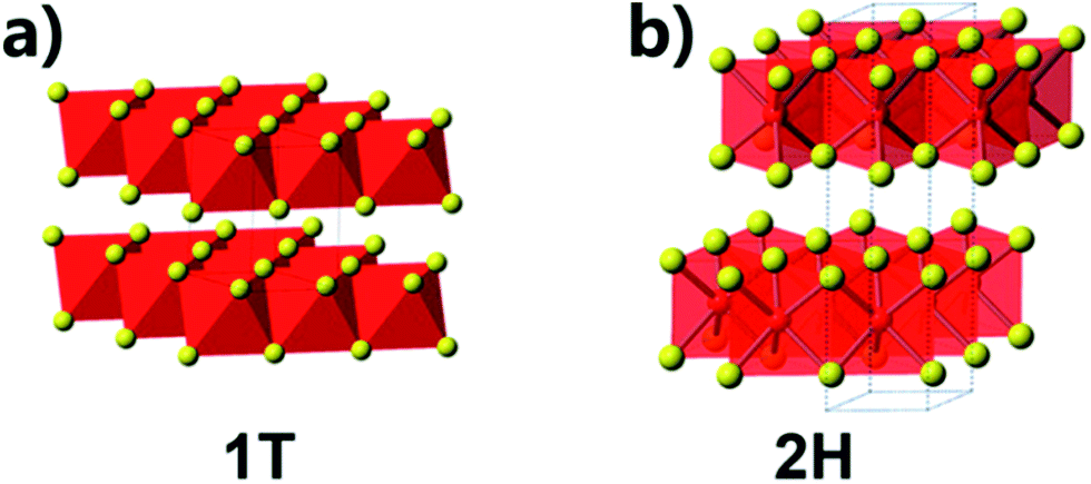 | ||
| Fig. 1 Crystal structures of (a) 1T and (b) 2H crystal structures of the TMDs. Adapted with permission from ref. 6. Copyright 2013 American Chemical Society. | ||
Semiconducting TMDs such as MoS2 and WS2 with a tuneable band gap promote their applications in photoelectric field.9,65,66 With decreasing layer number, the band gap present an increasing trend, and the indirect band gap of bulk TMDs gradually shift to be direct when reduced to single layer.67 Fig. 2 shows a band structure of bulk and monolayer MoS2 calculated from first principles.68 At the Γ-point, bulk MoS2 has an indirect band gap of 1.2 eV, which can be transferred to a direct band gap of 1.9 eV in monolayer form. This phenomenon can be explained by quantum confinement effect.14,69 Owing to the direct band gap, a strong PL is observed in monolayer MoS2, and the PL quantum yield (QY) has a 104 fold enhancement compared with their bulk crystal.70 Moreover, the PL of monolayer MoS2 can be effectively improved via an air-stable, solution-based chemical treatment and the consequent QY is more than 95%.71 Therefore, single layer semiconducting TMDs with direct band gap indicates that they are promising candidates in optoelectronic applications.72
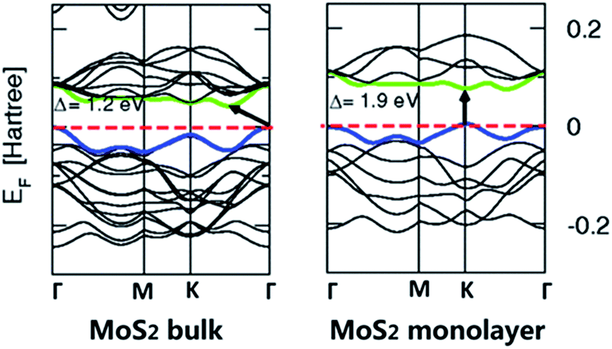 | ||
| Fig. 2 Band structures of bulk MoS2 and its monolayer. The arrows indicate the smallest value of the band gap (direct or indirect) for a given system. The top of valence band (blue) and bottom of conduction band (green) are highlighted. Adapted with permission from ref. 68. Copyright 2011 by the American Physical Society. | ||
2.3 LDNs/TMDs heterostructures
The integration of materials in different dimensionalities is able to combine the inherent advantages and mitigate the genetic disadvantages in terms of fundamental properties.73 Noble metals, metal oxides, graphite derivatives crystals with sizes in nanoscale such as Au NPs and carbon NTs (CNTs) can be integrated with 2D TMDs NSs. The as-prepared heterostructures present an obviously enhanced performance in electrical and optical application.74–77 For instance, Zhou et al. prepared TiO2 NBs@MoS2 NSs heterostructure via a hydrothermal reaction, and the heterostructure exhibits highly photocatalytic hydrogen production.78 Herein, the synergistic effect of TiO2 and MoS2 resulting in the heterostructure provides efficient charge separation to suppress the electron–hole recombination, and further display an improved photocatalytic activity. In another case, Zhang et al. reported a hydrothermal method to fabricate a ZnO NRs/MoS2 NSs heterostructure without a catalyst.79 Due to the light antennae effect of ZnO NRs, enhanced Raman and PL emission are observed in this type of heterostructure.According to the dimension of nanostructures, these heterostructures can be divided into 0D/2D and 1D/2D, as shown in Fig. 3. Generally, 0D nanostructures usually tiled on TMDs NSs, and 1D nanostructure usually served as an axis for TMDs NSs, which were loaded on their surface in form of 1D/2D.21,80–82 Every individual structure in these heterostructures plays an important role and contributes to tailored performance of the whole system. Layered TMDs have several crystal phases with different lattice structures and electronic character such as 1T and 2H, although integrated with the same LDNs, these heterostructures exhibit distinct performance.83,84 Bai et al. demonstrated that TiO2–MoS2 (1T) hybrid structure exhibited excellent performance as a co-catalyst to product hydrogen, which is in sharp contrast to TiO2–MoS2 (2H).85 This can be attributed to the active sites on the 1T-MoS2 basal plane, which gives rise to a high charge diffusion rate and reduces the probability of charge recombination when integrated with TiO2. On the contrary, 2H-MoS2 does not provide reaction sites and may block the active sites on the TiO2 nanocrystals surface. In addition, the layer numbers can affect the electrical and optical properties of TMDs. For example, monolayer MoS2 has a large enhancement of the luminescence compared with the bulk material.13 Therefore, layer number and crystal phase of TMDs are indispensable considerations when integrated with LDNs. Besides, the morphology and distribution of LDNs have impact on the system performance.86,87 For instance, Wang et al. prepared various morphologies of spherical, triangle, clover-like and flower-like AuNPs (Fig. 4) by changing the ratio of MoS2 and thionine (Thi), and demonstrated the clover-like Au NP/Thi–MoS2 nanocomposites-based electrochemical immunosensor exhibit an excellent selectivity, which can detect carcino-embryonic antigen (CEA) as low as 0.52 pg mL−1.88
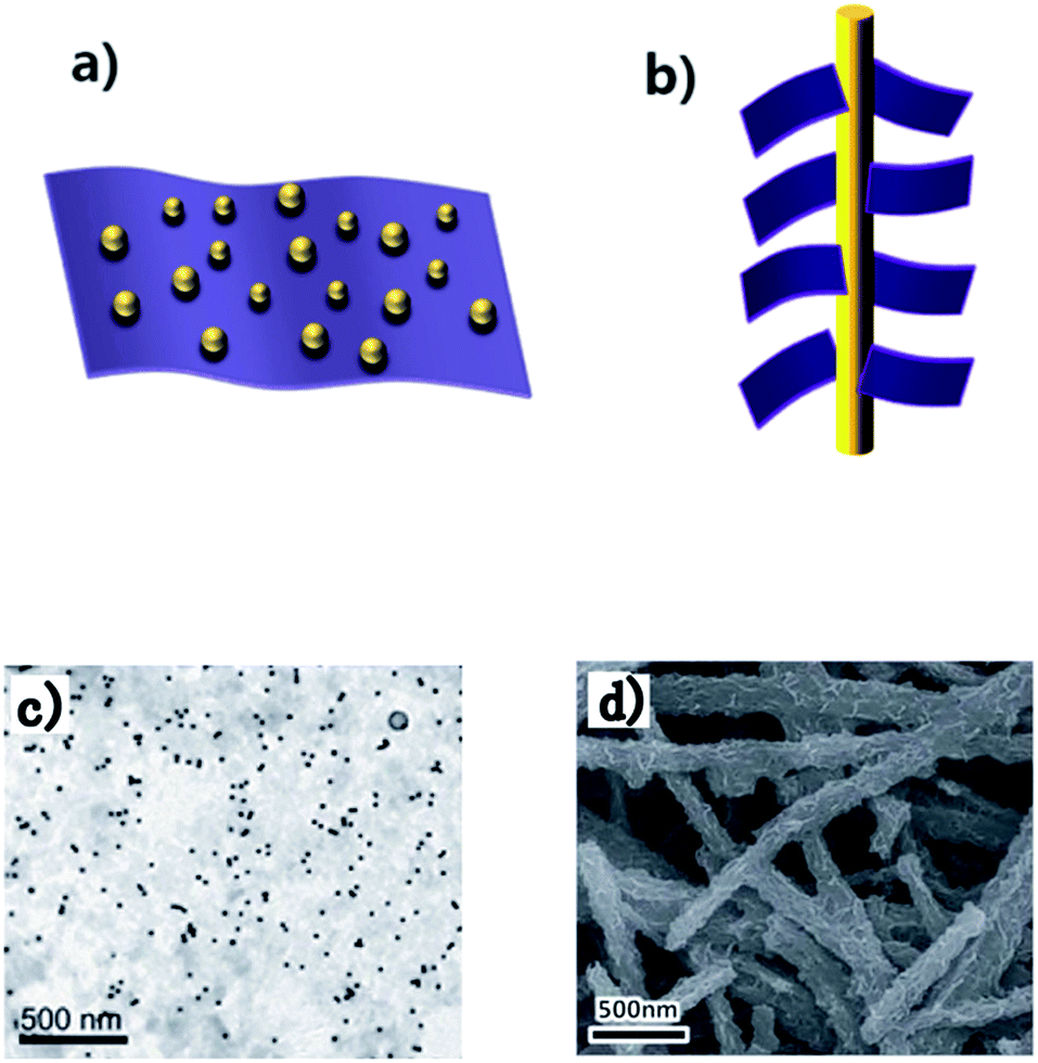 | ||
| Fig. 3 Schematic of integrated heterostructure (a) 0D/2D and (b) 1D/2D. SEM images of (c) 0D Au NPs/2D MoS2 NSs and (d) 1D TiO2 NBs/2D MoSe2 NSs. Adapted from ref. 75 and 89 with permission of The Royal Society of Chemistry. | ||
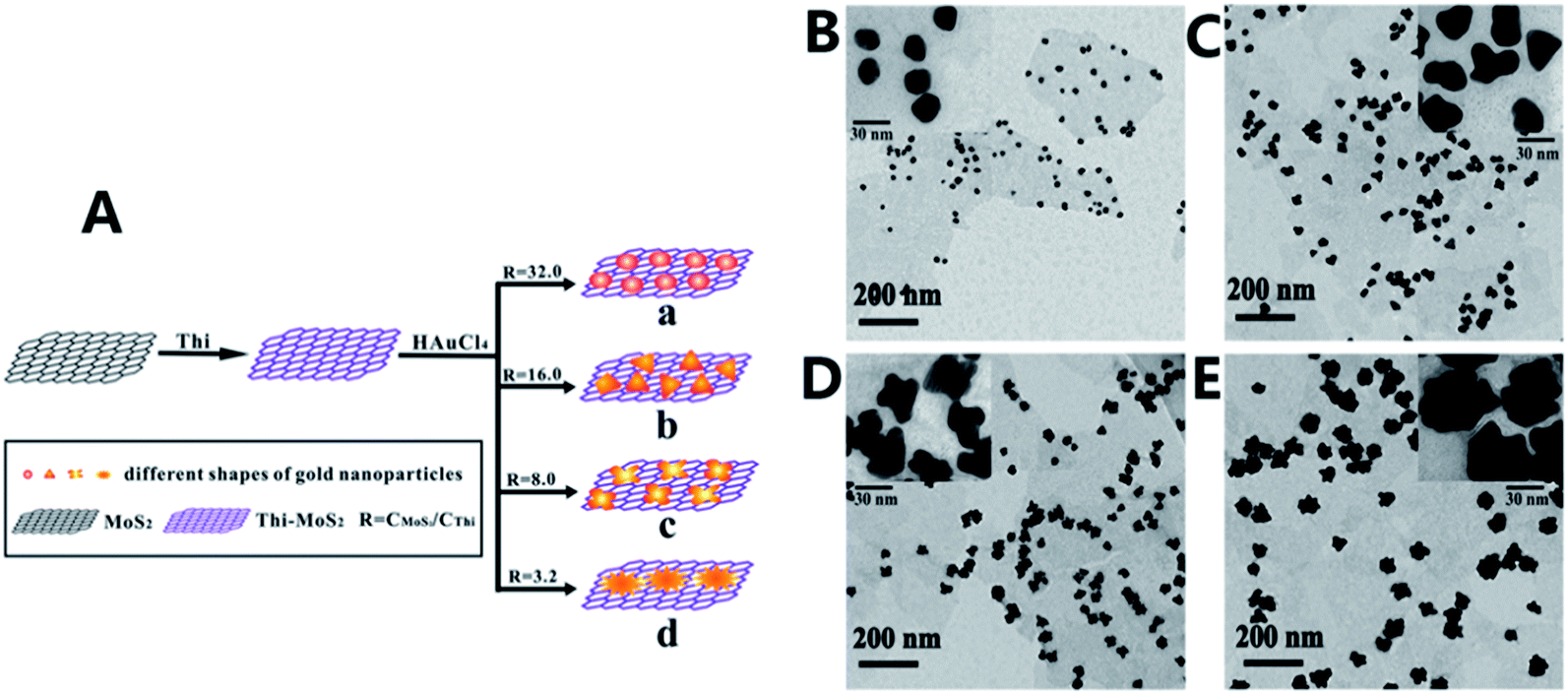 | ||
| Fig. 4 (A) Schematic of preparation process of shape-controlled Au NPs supported on Thi–MoS2 NSs. TEM images of AuNP–Thi–MoS2 nanocomposites with (B) spherical, (C) triangle, (D) clover-like and (E) flower-like AuNPs. Adapted from ref. 88 with permission of The Royal Society of Chemistry. | ||
3. Synthesis methods
Preparation of high quality TMDs NSs is an important process in their heterostructures fabrication. Both physical and chemical methods can be considered to obtain layered TMDs, such as exfoliation and chemical vapor deposition (CVD).21,90–94 For the synthesis of integrated nanostructures, different approaches have already been developed, as concluded in Table 1, which can be classified into two main methods: self-assembly and hydrothermal/solvothermal.| Dimensionality | Synthesis methods | Integrated nanostructures | Applications | Ref. |
|---|---|---|---|---|
| 0D/2D | Self-assembly | Ag NPs–WS2 | Supercapacitor | 102 |
| Au NPs–MoS2 | Sensor | 103 | ||
| TiO2 NPs–MoS2 | Hydrogen production | 85 | ||
| Hydrothermal | TiO2–RGO–MoS2 | Hydrogen production | 104 | |
| ZnO–MoS2 | Hydrogen production | 105 | ||
| SnO2–MoS2 | Sensor | 106 | ||
| Solvothermal | GQDs–MoS2 | LIBs | 107 | |
| Electrodeposition | Au NPs–MoS2 | Sensor | 108 | |
| Thermal evaporation | Au NPs–MoS2 | Sensor or detector | 82 | |
| Drop casting | Pd NPs–MoS2 | Sensor | 109 | |
| Successive ion layer adsorption and reaction method | CdS NPs–WS2 | Water splitting | 110 | |
| 1D/2D | Self-assembly | Au NRs–MoS2 | Hydrogen production | 111 |
| Hydrothermal | C/TiO2 NBs–MoSe2 | LIBs | 89 | |
| CoS2 NWs–MoS2 | Hydrogen production | 112 | ||
| Solvothermal | CNTs–MoS2 | Hydrogen production | 77 | |
| SnO2 NTs–MoS2 | Hydrogen production | 113 |
3.1 Layer TMDs
To date, exfoliation of layered solid and CVD growth method are mainstream strategies to obtain layered TMDs. Typically, mechanical exfoliation use micromechanical force to separate bulk materials and obtain single or few layers NSs, but the yield is relatively low and the size is quite small.60 In comparison, chemical exfoliation can conquer these problems and obtain large-scale TMDs NSs. Zheng et al. used metal naphthalenide as intercalating agents to exfoliate metal chalcogenides and obtained high quality sheets with large size up to 400 μm2.95 The size distribution of the flakes is much better than the sheets obtained by using organolithium salts, and the prepared TMDs sheets could be directly jet-printed on substrate. Shear exfoliation can also prepare TMDs NSs by separating bulk materials. Varrla et al. demonstrated the processing parameters for specific NSs concentration, length, and thickness and obtained large-scale shear-exfoliation of MoS2 NSs (in the range ∼40–220 nm for length and ∼2–12 layers for thickness) in aqueous surfactant solution by using a kitchen blender.96 CVD is a typical method to prepare high-quality TMDs layers with controllable thickness and scalable size.90 Lee et al. has utilized CVD approach to synthesis large-area MoS2 NSs with six-fold symmetry hexagonal lattice and high crystallinity on SiO2/Si substrates.97 In addition to preparing layered TMDs with certain thickness, CVD growth method provide a facile way to directly grow layered heterostructures, which eliminates interfacial contamination interfused during synthesis processes.98 Moreover, wet chemical approach is another available method to prepared layered TMDs, which can be directly obtained in solution with a high yield.99 However, improved purity and controllability over nanostructures are primary challenges because of infancy.100,101 In general, chemical exfoliation is desirable method for mass production of TMDs NSs, because other methods usually have more or less limitations to some extent, such as low efficiency, long and complex process, requirement for expensive systems and severe synthetic conditions.1143.2 LDNs/TMDs nanostructures
Self-assembly is also available for metal oxide/TMDs heterostructure synthesis. Bai et al. prepared a TiO2–MoS2 (1T) hybrid structure via sonication.85 The typical procedure is mixing the dispersion of MoS2 NSs with aqueous dispersion of TiO2 nanocrystals and then sonicated for 3 min. In another case, Sun et al. prepared a p-type semiconductor of Cu2O decorated with MoS2 NSs by using hexadecyl trimethylammonium bromide (CTAB) as the surfactant to control the morphology.117 As-prepared nanocomposite exhibits efficient solar hydrogen production under visible light.
Size distribution, morphology and density of metal NPs can be tuned by changing the defects density in TMDs layers.87,118 Lu et al. reported that a focused laser beam can achieve active surface domains in MoS2 film, and the size of as-prepared Au NPs are controllable, which were preferentially decorated onto the modified regions.103 The rough surface of laser-pruned MoS2 could trap the precursor and provide initial nucleation sites for Au NP growth.
CNTs/TMDs heterostructure is widely studied in recent years due to their remarkable catalytic activity.77,122,123 Using in situ solid and hydrothermal reactions, Zhang et al. prepared Mo2C-embedded N-doped CNTs/MoS2 nanostructure.124 In MoO2/Mo2C-NCNTs aqueous solution, O2− ions are replaced with S2− ions which resulted in the transformation of MoO2 to MoS2. Metal oxide/TMDs nanocomposites can be prepared through this method as well. Li et al. demonstrated that with the assistance of glucose, TiO2 NWs can act as a backbone for the nucleation and growth of MoS2 NSs.125 As a binder, glucose suppressed the growth and stack of layered MoS2, facilitating the growth of MoS2 NSs with smaller sizes on the TiO2 NWs surface.125,126 Liu et al. prepared a SnO2@MoSe2 nanostructure through facile electrospinning technique and solvothermal method.127 SnO2 NFs are first obtained via a simple electrospinning method, then mixed with Se solution and dispersed in Na2Mo4 solution, which is subsequently heated to 180 °C and maintained for 12 h. The black precipitates of SnO2@MoSe2 after natural cooling exhibit excellent electrochemical activity as catalyst.
Wu et al. reported a green technique to prepare the WS2 and MoS2 QDs/NSs composites by sonication and solvothermal treatment.114 Typically, bulk MoS2/WS2 powders were sonicated in N-dimethylformamide for 3 h, and then stirred the top 2/3 of the dispersion for 6 h at 140 °C. After settled the suspensions for several hours, the light yellow supernatant of MoS2/WS2 QDs and the centrifugate of composite of MoS2/WS2 QDs and NSs composites were separated. In addition, Li et al. prepared a new type of 1D/2D heterostructures: GeS NWs are grown as seeds followed by GeS NSs epitaxially growing at the pre-grown NWs.73 The pre-grown NWs exposing to air caused a mild degree of oxidation at the NW surface, which could prompt the nucleation of the NSs. This strategy opens a novel avenue to synthesis NWs/NSs heterostructures.
4. Applications
4.1 Hydrogen production
Hydrogen is regarded as a potential fuel in the future to address the environmental crises and energy shortage issues.128,129 Utilizing electricity to split water is a green and effective approach to produce hydrogen. In general, it can be divided into two strategies: electrocatalytic and photoelectrocatalytic.130,131 Noble metals such as Pt, Pd, Ru and Au are widely known as effective electrochemical catalysts due to their excellent catalytic activity.132 Pt and its alloys have usually been the first choice of catalysts, however, scarcity and high cost severely hinder its practical application.133,134 TMDs are regarded as ideal candidates to replace Pt due to high chemical stability and excellent electrocatalytic properties.135 For instance, nanoscale MoS2 exhibits a good reduction capacity for protons due to the quantum confinement effect, and the marginal edges served as active sites can promote the decomposition of water.76 Xie et al. demonstrated defect-rich MoS2 NSs could present excellent hydrogen evolution reaction (HER) activity with a low onset overpotential of 120 mV and small Tafel slope of 50 mV dec−1.136 However, low conductivity of TMDs largely limited the charge transfer rate and affected the total efficiency.137 An efficient way to address this issue is integrating TMDs nanostructures with conductive substrates,124 such as graphene, carbon NTs or carbon NFs. Guo et al. prepared a N-doped CNFs/defect and S-rich MoS2 heterostructure for high efficiency HER with a small overpotential of 135 mV at 10 mA cm−2 and a large cathodic current density of 65.6 mA cm−2 at 200 mV (Fig. 5).122 Nitrogen doping promoted the conductivity of composites, and the embedded mode of MoS2 NSs and CNFs greatly improved their stability and catalytic activity. CoS2 NW/MoS2 NSs supported on carbon cloth also exhibits excellent HER performance and prominent electrochemical durability.112 However, most of the conductive substrates are inert for the HER and will decrease the density of active sites of TMDs NSs, therefore, balancing the active sites and conductivity of electrochemical catalysts remains a knotty problem.124 On the other hand, integrated with noble metal nanostructures, TMDs can achieve a high electrocatalytic performance toward HER.138 For instance, Au NPs coated on TMDs NSs can largely improve the charge transport along interplanar directions and inhibited restacking, which improved the accessibility of protons to the catalytically active sites.118 Hou et al. reported the growth of Pt NPs/MoS2 NSs on the surface of carbon fiber and demonstrated an overpotential of −5 mV and a corresponding Tafel slope of 53.6 mV dec−1.139 The large specific surface area of TMDs not only effectively collect and transport charges, but also provides plenty of nucleation sites for the growth of metal NPs.138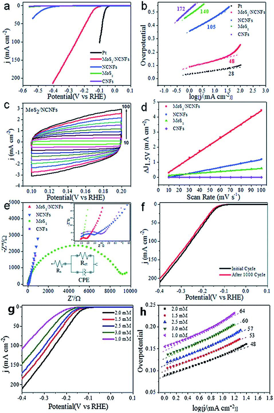 | ||
| Fig. 5 Electrocatalytic performance of MoS2/NCNFs. (a) Polarization curves, (b) Tafel plots, (c) electrochemical cyclic voltammogram of MoS2/NCNFs at different potential scanning rates, (d) the Cdl of different materials obtained at 0.15 V vs. RHE, (e) Nyquist plots and (f) stability of the MoS2/NCNFs with the initial polarization curve (black curve) and after 1000 cycles (red curve). (g) Polarization curves (g) and (h) the corresponding Tafel plots of MoS2/NCNFs prepared at different concentration of Mo precursor. Adapted from ref. 122 with permission of The Royal Society of Chemistry. | ||
In 1972, Fujishima et al. demonstrated a green approach to split water utilizing TiO2 as a photochemical catalyst, which offers a promising way for clean and low-cost production of hydrogen via solar energy.140,141 However, the rapid recombination of the electron–hole pairs and low activation ability of the surface reduced the amount of charge, resulting in a low photocatalytic efficiency.85 Introducing TMDs as co-catalysts which serve as the reaction sites can promote the charge separation and transport.105 Indeed, MoS2 NSs coated on a TiO2 surface significantly facilitated the separation of the photo-induced carriers, which resulted in a higher photocurrent and improved broad spectrum photocatalytic properties.142,143 Moreover, Zhou et al. demonstrated that nitrogen self-doped MoS2 NSs integrated with MnO2 NBs exhibited excellent performance with an onset potential of −156 mV (vs. RHE), a large current density, a small Tafel slope of 47.5 mV dec−1 and outstanding electrochemical durability.144 Nitrogen doping provides a localized state near the Fermi energy in MoS2 band gap and thus leads to a high electronic conductivity of the heterostructure. Besides, electron-rich sites are beneficial to attract H+ to the catalyst surface and gains an enhanced HER activity. Plasmon-excited hot electrons injection mechanism is also an efficient and promising route for the improvement of catalyst activity.111 However, achieving a faster electrons injection from plasmonic metal to semiconductor than the recombination process is still a significant challenge.
4.2 Lithium battery
Rechargeable Li batteries with high energy density, good cycle life, and blameless power performance has become one of the most important energy storage devices in recent years.145 To date, silicon, metal alloys, metal oxides and TMDs have been widely explored as the replacement of graphite anodes in Li-ion batteries (LIB).146–148 The high surface-to-volume ratio and short diffusion path of TMD NSs render it as a brilliant electrode material for LIBs. For instance, Hwang et al. reported graphene-like MoS2 nanoplates showing a reversible capacity of 912 mA h g−1 at a rate of 1C and excellent cycling stability when fabricated in LIBs.149 To further improve the cycling stability and rate capability performance of TMDs, integrating LDNs such as Au NPs and TiO2 NPs is an effective approach.120,150 Guo et al. demonstrated that GQDs/MoS2 exhibits excellent electrochemical lithium storage properties with a high reversible capacity (1099 mA h g−1 at 100 mA g−1), good cyclic stability, as well as excellent rate performance (660 mA h g−1 at 5000 mA g−1) as shown in Fig. 6.107 GQDs acted as binder enhanced cyclic stability and facilitate the charge transfer within the electrode. Furthermore, it can enlarge the interlayer distance between MoS2 layers which is beneficial for Li+ intercalation. Zhou et al. demonstrated that CNFs@MoS2 coaxial NFs showed an excellent Li storage properties, such as high specific capacity, good cycling stability, and superior high-rate capability.151 The synergistic effect of the two active components leads to a larger capacity and better cyclability.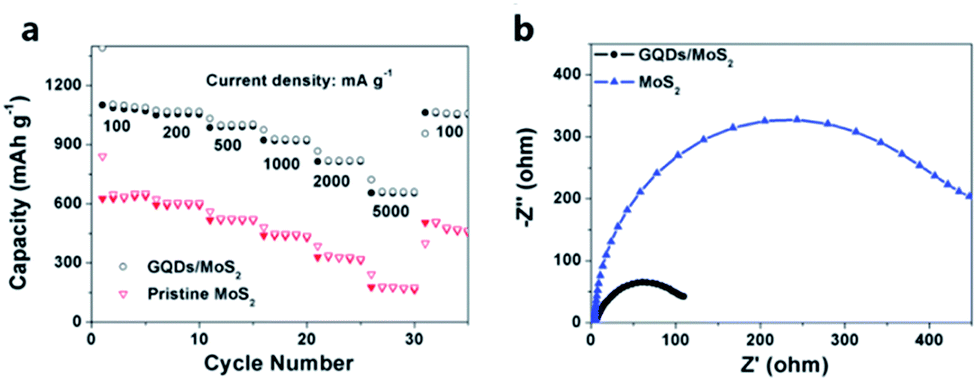 | ||
| Fig. 6 (a) Rate capabilities and (b) electrochemical impedance spectroscopy spectra of GQDs/MoS2 and pristine MoS2 electrodes. Adapted from ref. 107 with permission of The Royal Society of Chemistry. | ||
TiO2 with superior safety and rate capability exhibits excellent performance when employed as anodes materials.152 Li et al. demonstrated that TiO2@MoS2 heterostructure displayed a high initial discharge capacity of 862 mA h g−1, and it maintained at 544 mA h g−1 even after 100 cycles.125 The synergistic effects of TiO2 NW and ultrathin MoS2 shorten the Li+ diffusion paths for rapid charge transfer, and improved cycling stability of the system at high rates. Xue et al. demonstrated a Fe3O4 NPs/MoS2 nanostructures as an anode for LIBs with a superior cyclic and rate performances.153 Fe3O4 NPs serving as spacers and effectively stabilize the integrated structure, facilitating the MoS2 surfaces accessible to electrolyte during charge/discharge processes, thereby hindering the fast fading of reversible capacities. The heterostructure contribute a 1033 and 224 mA h g−1 at current densities of 2000 and 10![[thin space (1/6-em)]](https://www.rsc.org/images/entities/char_2009.gif) 000 mA g−1, respectively. The MoS2 NSs provided a high reversible capacity and Fe3O4 NPs offered a high rate performance. In addition, MoS2 has been reported as cathode material for lithium–oxygen (Li–O2) batteries, which exhibits a 85% round-trip efficiency and good reversibility.159 Table 2 lists some typical examples comprised of different components for lithium storage performances.
000 mA g−1, respectively. The MoS2 NSs provided a high reversible capacity and Fe3O4 NPs offered a high rate performance. In addition, MoS2 has been reported as cathode material for lithium–oxygen (Li–O2) batteries, which exhibits a 85% round-trip efficiency and good reversibility.159 Table 2 lists some typical examples comprised of different components for lithium storage performances.
| Anode materials | Current rate | Initial capacity (mA h g−1) | Capacity retention (mA h g−1)/(cycles) | Ref. |
|---|---|---|---|---|
| MoS2 | 1C | 1062 | 907/50 | 149 |
| Graphene–MoS2 | 100 mA g−1 | 1571 | 1187/100 | 154 |
| CNFs–MoS2 | 100 mA g−1 | 1489 | 1264/50 | 151 |
| GQDs-MoS2 | 100 mA g−1 | 1394 | 1031/80 | 107 |
| TiO2–MoS2 | 0.1C | 588 | 350/100 | 155 |
| Carbon–TiO2–MoS2 | 100 mA g−1 | 941.6 | 805/100 | 156 |
| Polyaniline–MoS2 | 100 mA g−1 | 1063.9 | ∼953/50 | 157 |
| SnO2–MoS2 | 0.2C | 1306 | ∼900/80 | 158 |
TMDs anodes have been studied for many years, yet there are still many challenges. The large irreversible capacity was observed in the first cycle, indicating that a large portion of Li+ ions could not be utilized again in the following cycles, and the relatively high voltage behavior of the TMDs limited its applications.160 Nevertheless, TMDs is a promising anodes material owing to superior capacity and rate capability.8
4.3 Sensor and detector
TMDs materials with a tuneable band gap applied in sensors and detectors usually exhibited high selectivity and rapid detection.161–164 Using first-principles calculations, Yue et al. found that small gas molecules can be physically absorbed on monolayer MoS2, and determined the most stable adsorption configuration and adsorption energy.165 The band structure of monolayer MoS2 will not significantly be altered though small gas molecules are absorbed. Many reports have demonstrated TMDs-based sensors, when integrated with noble metal or metal oxide semiconductors, exhibiting an enhanced performance compared with individual component.166–168 For instance, He et al. demonstrated that Pt NPs deposited on MoS2 NSs exhibits high sensitivity for NO2 detection.169 Upon the adsorption of gas, the Schottky barrier between Pt NPs and MoS2 channel is changed, which may help explain the increased sensitivity of MoS2 thin film.170,171 In addition, Kuru et al. demonstrated Pd NPs/MoS2 NS could show a highly sensitivity for H2 detection at room temperature and the sensor exhibits a response of around 10 toward 50000 ppm H2 with a response and recovery time of 40 and 83 s, respectively.109 TMDs-based biosensor can effectively and sensitively detect biomolecule.172,173 Using molecular dynamics and density functional theory simulation, Aluru et al. demonstrated that monolayer MoS2 is an promising material for DNA sequencing technology.174 Thiol modified monolayer MoS2 integrated with Au NPs can largely enhance the DNA adsorption about 1 order of magnitude.175 MoS2 NSs exhibited different PL properties toward single-strained DNA versus double strained DNA when the concentration of DNA solution increased, which can be used for rapid and selective detection of DNA nucleoside chains. In another case, Su et al. reported a Au NPs/MoS2 biosensor that could detect glucose in a concentration range from 10 to 300 μM with a detection limit of 2.8 μM.176 Furthermore, the sensor also displays good reproducibility and long-term stability, indicating its potential to be applied for determination of glucose concentration in human serum. In addition, Shao et al. reported an electrochemical dopamine (DA) sensor based on Au NPs@MoS2 nanocomposite, and the detection concentration of DA ranges from 0.1 to 200 mM, with a detection limit of 80 nM (S/N = 3),121 and the sensor can also detect DA in ascorbic acid existed environment.
Monolayer MoS2 with a direct bandgap of 1.9 eV is extremely attractive for photodetector. Kis et al. reported a monolayer MoS2 photodetector with a photoresponsivity of 880 A W−1 at a wavelength of 561 nm and a photoresponse in the 400–680 nm range.177 However, the slow responsivity is an important limiting factor for application. To address this situation, Kufer et al. demonstrated PbS QDs decorated MoS2 for photodetector could achieve a high responsivity of 6 × 10⁵ A W−1, and the responsivity is higher than individual PbS QDs and MoS2-based detectors.178 Owing to the effect of reverse electric induced by increasing separated charge carriers, the responsivity presents a decrease trend with increasing optical intensity. In addition, metal plasmon LDNs with near-field oscillation and scattering effect can effectively improve the photocurrent response and light absorption of TMDs, which can be applied to exploit plasmon resonance-based devices.179 Although great progress has been made in this area, the mechanism and principles of electron transfer of TMDs is remain unclear.180
5. Conclusion
In summary, the integration of LDNs and TMD exhibits a tailored performance due to synergistic effects. LDN materials with dissimilar properties that differ from their bulk counterparts effectively mitigate the genetic disadvantages of TMDs, while TMD NSs with controllable size and thickness provided suitable surface areas for LDNs to integrate. For LDN/TMD heterostructures, many synthesis methods such as self-assembly and hydrothermal methods have been developed for preparation via one step or multi-step approaches. The shape and distribution of LDNs can be controlled by changing the component ratio of precursor solution or modifying the surface of TMDs and have a large impact on the system performance. Through incorporating different types of LDNs, TMD heterostructures with unique properties have been applied in various areas. As a promising candidate to replace Pt catalyst for hydrogen production, TMDs integrated with LDNs solve the limitation of low conductivity, and shows a high chemical stability and excellent electrocatalytic activities. As electrode materials for LIBs, the heterostructure contributes a high reversible capacity and an excellent rate capability. Owing to the high surface-to-volume ratio and tuneable band gap of TMDs, the sensors combine with LDNs exhibit a high selectivity to detect biomolecules and gas molecules, and have great impacts in the field of photodetection.Although extensive investigations have focused on LDNs/TMDs heterostructures, several limitations still exist. Firstly, LDNs reported in most papers are noble metals, metal oxides, metal dichalcogenides and graphite derivatives, the fields may expand to organic materials in future. Secondly, a method to prepare TMD NSs with excellent morphology and desired properties is still necessary. Heteroatom doping can offer TMDs with various new or improved optical and structural properties,181 which may provide some inspiration for further development of LDNs/TMDs heterostructures. Finally, how the spatial organization and distribution affecting the system performances have not been fully investigated yet.182 Many reports are restricted to concern the component of the heterostructure, therefore more studies are still required to optimize the fabricated structures. Nonetheless, the study of TMDs is just in the infant stage and a greater potential is waiting for exploration.
Acknowledgements
The authors gratefully acknowledge funding from National Natural Science Foundation of China 51272038, National Natural Science Foundation of China 51302030, National Natural Science Foundation of China 61474015 and National Program on Key Basic Research Project (973 Program) 2013CB933301.References
- F. Bonaccorso, L. Colombo, G. Yu, M. Stoller, V. Tozzini, A. C. Ferrari, R. S. Ruoff and V. Pellegrini, Science, 2015, 347, 1246501 CrossRef PubMed.
- X. Wang, G. Sun, P. Routh, D. H. Kim, W. Huang and P. Chen, Chem. Soc. Rev., 2014, 43, 7067–7098 RSC.
- F. Xia, H. Wang, D. Xiao, M. Dubey and A. Ramasubramaniam, Nat. Photonics, 2014, 8, 899–907 CrossRef CAS.
- D. Jariwala, V. K. Sangwan, L. J. Lauhon, T. J. Marks and M. C. Hersam, ACS Nano, 2014, 8, 1102–1120 CrossRef CAS PubMed.
- M. Xu, T. Liang, M. Shi and H. Chen, Chem. Rev., 2013, 113, 3766–3798 CrossRef CAS PubMed.
- S. Z. Butler, S. M. Hollen, L. Cao, Y. Cui, J. A. Gupta, H. R. Gutiérrez, T. F. Heinz, S. S. Hong, J. Huang, A. F. Ismach, E. Johnston-Halperin, M. Kuno, V. V. Plashnitsa, R. D. Robinson, R. S. Ruoff, S. Salahuddin, J. Shan, L. Shi, M. G. Spencer, M. Terrones, W. Windl and J. E. Goldberger, ACS Nano, 2013, 7, 2898–2926 CrossRef CAS PubMed.
- L. Tao, D. Wang, S. Jiang, Y. Liu, Q. Xie, H. Tian, N. Deng, X. Wang, Y. Yang and T.-L. Ren, J. Semicond., 2016, 37, 041001 CrossRef.
- H. Li, Y. Shi, M.-H. Chiu and L.-J. Li, Nano Energy, 2015, 18, 293–305 CrossRef CAS.
- V. Sorkin, H. Pan, H. Shi, S. Y. Quek and Y. W. Zhang, Crit. Rev. Solid State Mater. Sci., 2014, 39, 319–367 CrossRef CAS.
- M. Chhowalla, H. S. Shin, G. Eda, L. J. Li, K. P. Loh and H. Zhang, Nat. Chem., 2013, 5, 263–275 CrossRef PubMed.
- L. Yuwen, F. Xu, B. Xue, Z. Luo, Q. Zhang, B. Bao, S. Su, L. Weng, W. Huang and L. Wang, Nanoscale, 2014, 6, 5762–5769 RSC.
- J. A. Wilson and A. D. Yoffe, Adv. Phys., 1969, 18, 193–335 CrossRef CAS.
- K. F. Mak, C. Lee, J. Hone, J. Shan and T. F. Heinz, Phys. Rev. Lett., 2010, 105, 136805 CrossRef PubMed.
- Q. H. Wang, K. Kalantar-Zadeh, A. Kis, J. N. Coleman and M. S. Strano, Nat. Nanotechnol., 2012, 7, 699–712 CrossRef CAS PubMed.
- X. Tong, E. Ashalley, F. Lin, H. Li and Z. M. Wang, Nano-Micro Lett., 2015, 7, 203–218 CrossRef.
- A. K. Geim and I. V. Grigorieva, Nature, 2013, 499, 419–425 CrossRef CAS PubMed.
- H. Wang, F. Liu, W. Fu, Z. Fang, W. Zhou and Z. Liu, Nanoscale, 2014, 6, 12250–12272 RSC.
- J. Kang, J. Li, S. S. Li, J. B. Xia and L. W. Wang, Nano Lett., 2013, 13, 5485–5490 CrossRef CAS PubMed.
- N. Myoung, K. Seo, S. J. Lee and G. Ihm, ACS Nano, 2013, 7, 7021–7027 CrossRef CAS PubMed.
- H. Zheng, Y. Li, H. Liu, X. Yin and Y. Li, Chem. Soc. Rev., 2011, 40, 4506–4524 RSC.
- B. Luo, G. Liu and L. Wang, Nanoscale, 2016, 8, 6904–6920 RSC.
- W. T. Sun, Y. Yu, H. Y. Pan, X. F. Gao, Q. Chen and L. M. Peng, J. Am. Chem. Soc., 2008, 130, 1124–1125 CrossRef CAS PubMed.
- A. Cao, Z. Liu, S. Chu, M. Wu, Z. Ye, Z. Cai, Y. Chang, S. Wang, Q. Gong and Y. Liu, Adv. Mater., 2010, 22, 103–106 CrossRef CAS PubMed.
- H. Kim and K. Yong, Phys. Chem. Chem. Phys., 2013, 15, 2109–2116 RSC.
- H. Zhao, G. Sirigu, A. Parisini, A. Camellini, G. Nicotra, F. Rosei, V. Morandi, M. Zavelani-Rossi and A. Vomiero, Nanoscale, 2016, 8, 4217–4226 RSC.
- E. A. Anyebe, M. K. Rajpalke, T. D. Veal, C. J. Jin, Z. M. Wang and Q. D. Zhuang, Nano Res., 2014, 8, 1309–1319 CrossRef.
- G. Vasseur, Y. Fagot-Revurat, M. Sicot, B. Kierren, L. Moreau, D. Malterre, L. Cardenas, G. Galeotti, J. Lipton-Duffin, F. Rosei, M. Di Giovannantonio, G. Contini, P. Le Fevre, F. Bertran, L. Liang, V. Meunier and D. F. Perepichka, Nat. Commun., 2016, 7, 10235 CrossRef CAS PubMed.
- R. Brayner and F. Bozon-Verduraz, Phys. Chem. Chem. Phys., 2003, 5, 1457–1466 RSC.
- Y. Xia, P. Yang, Y. Sun, Y. Wu, B. T. Mayers, B. D. Gates, Y. Yin, F. Kim and H. Yan, Adv. Mater., 2003, 15, 353–389 CrossRef CAS.
- C. Frigerio, D. S. Ribeiro, S. S. Rodrigues, V. L. Abreu, J. A. Barbosa, J. A. Prior, K. L. Marques and J. L. Santos, Anal. Chim. Acta, 2012, 735, 9–22 CrossRef CAS PubMed.
- R.-H. Tao, J.-M. Wu, H.-X. Xue, X.-M. Song, X. Pan, X.-Q. Fang, X.-D. Fang and S.-Y. Dai, J. Power Sources, 2010, 195, 2989–2995 CrossRef CAS.
- W. Wen, J. M. Wu, Y. Z. Jiang, S. L. Yu, J. Q. Bai, M. H. Cao and J. Cui, Sci. Rep., 2015, 5, 11804 CrossRef PubMed.
- Z. Yin, B. Chen, M. Bosman, X. Cao, J. Chen, B. Zheng and H. Zhang, Small, 2014, 10, 3537–3543 CrossRef CAS PubMed.
- B. Li, J. M. Wu, T. T. Guo, M. Z. Tang and W. Wen, Nanoscale, 2014, 6, 3046–3050 RSC.
- D. Deng, K. S. Novoselov, Q. Fu, N. Zheng, Z. Tian and X. Bao, Nat. Nanotechnol., 2016, 11, 218–230 CrossRef CAS PubMed.
- X. Chia, A. Y. Eng, A. Ambrosi, S. M. Tan and M. Pumera, Chem. Rev., 2015, 115, 11941–11966 CrossRef CAS PubMed.
- F. Reale, K. Sharda and C. Mattevi, Applied Materials Today, 2016, 3, 11–22 CrossRef.
- Z. He and W. Que, Applied Materials Today, 2016, 3, 23–56 CrossRef.
- W. Guo, J. Yin, H. Qiu, Y. Guo, H. Wu and M. Xue, Friction, 2014, 2, 209–225 CrossRef CAS.
- J. Loomis and B. Panchapakesan, Nanotechnology, 2012, 23, 215501 CrossRef PubMed.
- K. Peng, Y. Xu, Y. Wu, Y. Yan, S. T. Lee and J. Zhu, Small, 2005, 1, 1062–1067 CrossRef CAS PubMed.
- P. Yu, J. Wu, S. Liu, J. Xiong, C. Jagadish and Z. M. Wang, Nano Today, 2016, 11, 704–737 CrossRef CAS.
- L. Hu and G. Chen, Nano Lett., 2007, 7, 3249–3252 CrossRef CAS PubMed.
- X. Huang, I. H. El-Sayed, W. Qian and M. A. El-Sayed, J. Am. Chem. Soc., 2006, 128, 2115–2120 CrossRef CAS PubMed.
- S. A. Maier and H. A. Atwater, J. Appl. Phys., 2005, 98, 011101 CrossRef.
- M. R. Jones, K. D. Osberg, R. J. Macfarlane, M. R. Langille and C. A. Mirkin, Chem. Rev., 2011, 111, 3736–3827 CrossRef CAS PubMed.
- J. Wu, P. Yu, A. S. Susha, K. A. Sablon, H. Chen, Z. Zhou, H. Li, H. Ji, X. Niu, A. O. Govorov, A. L. Rogach and Z. M. Wang, Nano Energy, 2015, 13, 827–835 CrossRef CAS.
- S. Eustis and M. A. El-Sayed, Chem. Soc. Rev., 2006, 35, 209–217 RSC.
- B. O. Dabbousi, J. Rodriguez-Viejo, F. V. Mikulec, J. R. Heine, H. Mattoussi, R. Ober, K. F. Jensen and M. G. Bawendi, J. Phys. Chem. B, 1997, 101, 9463–9475 CrossRef CAS.
- V.-V. Truong, P. Courteau and J. Singh, J. Appl. Phys., 1987, 62, 4863 CrossRef.
- X. Xue, W. Ji, Z. Mao, H. Mao, Y. Wang, X. Wang, W. Ruan, B. Zhao and J. R. Lombardi, J. Phys. Chem. C, 2012, 116, 8792–8797 CAS.
- Y. Cui, P. P. Shum, G. Y. Wang, H. Chang, X. Q. Dinh, M. Jiang and G. Humbert, Sensors, 2011, 371–374 Search PubMed.
- A. Convertino, M. Cuscunà, F. Martelli, M. G. Manera and R. Rella, J. Phys. Chem. C, 2014, 118, 685–690 CAS.
- P. Claus, A. Bruckner, C. Mohr and H. Hofmeister, J. Am. Chem. Soc., 2000, 122, 11430–11439 CrossRef CAS.
- D. M. Sagar, R. R. Cooney, S. L. Sewall, E. A. Dias, M. M. Barsan, I. S. Butler and P. Kambhampati, Phys. Rev. B: Condens. Matter Mater. Phys., 2008, 77 Search PubMed.
- D. Gao, H. Zhou, J. Wang, S. Miao, F. Yang, G. Wang, J. Wang and X. Bao, J. Am. Chem. Soc., 2015, 137, 4288–4291 CrossRef CAS PubMed.
- K. Das, K. Rawat, R. Patel and H. B. Bohidar, RSC Adv., 2016, 6, 46744–46754 RSC.
- P. Yu, J. Wu, E. Ashalley, A. Govorov and Z. Wang, J. Phys. D: Appl. Phys., 2016, 49, 365101 CrossRef.
- B. Hamawandi, M. Noroozi, G. Jayakumar, A. Ergül, K. Zahmatkesh, M. S. Toprak and H. H. Radamson, J. Semicond., 2016, 37, 102001 CrossRef.
- S. A. Han, R. Bhatia and S.-W. Kim, Nano Convergence, 2015, 2 Search PubMed.
- C. Xia and J. Li, J. Semicond., 2016, 37, 051001 CrossRef.
- W. Zhao, R. M. Ribeiro and G. Eda, Acc. Chem. Res., 2015, 48, 91–99 CrossRef CAS PubMed.
- Y. Kang, S. Najmaei, Z. Liu, Y. Bao, Y. Wang, X. Zhu, N. J. Halas, P. Nordlander, P. M. Ajayan, J. Lou and Z. Fang, Adv. Mater., 2014, 26, 6467–6471 CrossRef CAS PubMed.
- M. Acerce, D. Voiry and M. Chhowalla, Nat. Nanotechnol., 2015, 10, 313–318 CrossRef CAS PubMed.
- K. F. Mak, K. He, J. Shan and T. F. Heinz, Nat. Nanotechnol., 2012, 7, 494–498 CrossRef CAS PubMed.
- Z. Yin, H. Li, H. Li, L. Jiang, Y. Shi, Y. Sun, G. Lu, Q. Zhang, X. Chen and H. Zhang, ACS Nano, 2013, 6, 74–80 CrossRef PubMed.
- S. Bhattacharyya and A. K. Singh, Phys. Rev. B: Condens. Matter Mater. Phys., 2012, 86 Search PubMed.
- A. Kuc, N. Zibouche and T. Heine, Phys. Rev. B: Condens. Matter Mater. Phys., 2011, 83, 245213 CrossRef.
- A. Splendiani, L. Sun, Y. Zhang, T. Li, J. Kim, C. Y. Chim, G. Galli and F. Wang, Nano Lett., 2010, 10, 1271–1275 CrossRef CAS PubMed.
- K. F. Mak, C. Lee, J. Hone, J. Shan and T. F. Heinz, Phys. Rev. Lett., 2010, 105, 136805 CrossRef PubMed.
- M. Amani, D. Lien, D. Kiriya, J. Xiao, A. Azcatl, J. Noh, S. R. Madhvapathy, R. Addou, K. C. Santosh and M. Dubey, Science, 2015, 350, 1065–1068 CrossRef CAS PubMed.
- P. Tonndorf, R. Schmidt, P. Bottger, X. Zhang, J. Borner, A. Liebig, M. Albrecht, C. Kloc, O. Gordan, D. R. Zahn, S. Michaelis de Vasconcellos and R. Bratschitsch, Opt. Express, 2013, 21, 4908–4916 CrossRef CAS PubMed.
- C. Li, Y. Yu, M. Chi and L. Cao, Nano Lett., 2013, 13, 948–953 CrossRef CAS PubMed.
- B. Mukherjee and E. Simsek, Plasmonics, 2015, 11, 285–289 CrossRef.
- X. Yang, W. Liu, M. Xiong, Y. Zhang, T. Liang, J. Yang, M. Xu, J. Ye and H. Chen, J. Mater. Chem. A, 2014, 2, 14798 CAS.
- B. Zhu, B. Lin, Y. Zhou, P. Sun, Q. Yao, Y. Chen and B. Gao, J. Mater. Chem. A, 2014, 2, 3819 CAS.
- Y. Yan, X. Ge, Z. Liu, J. Y. Wang, J. M. Lee and X. Wang, Nanoscale, 2013, 5, 7768–7771 RSC.
- W. Zhou, Z. Yin, Y. Du, X. Huang, Z. Zeng, Z. Fan, H. Liu, J. Wang and H. Zhang, Small, 2013, 9, 140–147 CrossRef CAS PubMed.
- K. Zhang, Y. Zhang, T. Zhang, W. Dong, T. Wei, Y. Sun, X. Chen, G. Shen and N. Dai, Nano Res., 2014, 8, 743–750 CrossRef.
- X. Dai, K. Du, Z. Li, H. Sun, Y. Yang, W. Zhang and X. Zhang, Int. J. Hydrogen Energy, 2015, 40, 8877–8888 CrossRef CAS.
- M. Shen, Z. Yan, L. Yang, P. Du, J. Zhang and B. Xiang, Chem. Commun., 2014, 50, 15447–15449 RSC.
- U. Bhanu, M. R. Islam, L. Tetard and S. I. Khondaker, Sci. Rep., 2014, 4, 5575 CAS.
- K. K. Amara, Y. Chen, Y.-C. Lin, R. Kumar, E. Okunishi, K. Suenaga, S. Y. Quek and G. Eda, Chem. Mater., 2016, 28, 2308–2314 CrossRef CAS.
- B. Ouyang, Z. Mi and J. Song, J. Phys. Chem. C, 2016, 120, 8927–8935 CAS.
- S. Bai, L. Wang, X. Chen, J. Du and Y. Xiong, Nano Res., 2014, 8, 175–183 CrossRef.
- W. Cao, V. Pankratov, M. Huttula, X. Shi, S. Saukko, Z. Huang and M. Zhang, Mater. Chem. Phys., 2015, 158, 89–95 CrossRef CAS.
- Y. Shi, J. K. Huang, L. Jin, Y. T. Hsu, S. F. Yu, L. J. Li and H. Y. Yang, Sci. Rep., 2013, 3, 1839 Search PubMed.
- S. Su, M. Zou, H. Zhao, C. Yuan, Y. Xu, C. Zhang, L. Wang, C. Fan and L. Wang, Nanoscale, 2015, 7, 19129–19135 RSC.
- H. Wu, Y. Wu, X. Chen, Y. Ma, M. Xu, W. Wei, J. Pan and X. Xiong, RSC Adv., 2016, 6, 23161–23168 RSC.
- X. Wang, H. Feng, Y. Wu and L. Jiao, J. Am. Chem. Soc., 2013, 135, 5304–5307 CrossRef CAS PubMed.
- H. Li, X. Qi, J. Wu, Z. Zeng, J. Wei and H. Zhang, ACS Nano, 2013, 7, 2842–2849 CrossRef CAS PubMed.
- S. M. Tan, Z. Sofer, J. Luxa and M. Pumera, ACS Catal., 2016, 6, 4594–4607 CrossRef CAS.
- A. Ambrosi, Z. Sofer and M. Pumera, Small, 2015, 11, 605–612 CrossRef CAS PubMed.
- A. Ambrosi, Z. Sofer and M. Pumera, Chem. Commun., 2015, 51, 8450–8453 RSC.
- J. Zheng, H. Zhang, S. Dong, Y. Liu, C. T. Nai, H. S. Shin, H. Y. Jeong, B. Liu and K. P. Loh, Nat. Commun., 2014, 5, 2995 Search PubMed.
- E. Varrla, C. Backes, K. R. Paton, A. Harvey, Z. Gholamvand, J. McCauley and J. N. Coleman, Chem. Mater., 2015, 27, 1129–1139 CrossRef CAS.
- Y. H. Lee, X. Q. Zhang, W. Zhang, M. T. Chang, C. T. Lin, K. D. Chang, Y. C. Yu, J. T. Wang, C. S. Chang, L. J. Li and T. W. Lin, Adv. Mater., 2012, 24, 2320–2325 CrossRef CAS PubMed.
- X. Li and H. Zhu, Journal of Materiomics, 2015, 1, 33–44 CrossRef.
- R. Lv, J. A. Robinson, R. E. Schaak, D. Sun, Y. Sun, T. E. Mallouk and M. Terrones, Acc. Chem. Res., 2015, 48, 56–64 CrossRef CAS PubMed.
- J. T. Jang, S. Jeong, J. W. Seo, M. C. Kim, E. Sim, Y. Oh, S. Nam, B. Park and J. Cheon, J. Am. Chem. Soc., 2011, 133, 7636–7639 CrossRef CAS PubMed.
- S. Jeong, D. Yoo, J. T. Jang, M. Kim and J. Cheon, J. Am. Chem. Soc., 2012, 134, 18233–18236 CrossRef CAS PubMed.
- Y. Dai, X. H. Yan, X. Wu, D. W. Sha, M. Chen, H. Zou, J. Ren and X. N. Cheng, Mater. Lett., 2016, 173, 203–206 CrossRef CAS.
- J. Lu, J. H. Lu, H. Liu, B. Liu, L. Gong, E. S. Tok, K. P. Loh and C. H. Sow, Small, 2015, 11, 1792–1800 CrossRef CAS PubMed.
- D. B. Nimbalkar, H.-H. Lo, P. V. R. K. Ramacharyulu and S.-C. Ke, RSC Adv., 2016, 6, 31661–31667 RSC.
- Y. J. Yuan, F. Wang, B. Hu, H. W. Lu, Z. T. Yu and Z. G. Zou, Dalton Trans., 2015, 44, 10997–11003 RSC.
- H. Yan, P. Song, S. Zhang, Z. Yang and Q. Wang, RSC Adv., 2015, 5, 79593–79599 RSC.
- J. Guo, H. Zhu, Y. Sun, L. Tang and X. Zhang, J. Mater. Chem. A, 2016, 4, 4783–4789 CAS.
- H. Sun, J. Chao, X. Zuo, S. Su, X. Liu, L. Yuwen, C. Fan and L. Wang, RSC Adv., 2014, 4, 27625 RSC.
- C. Kuru, C. Choi, A. Kargar, D. Choi, Y. J. Kim, C. H. Liu, S. Yavuz and S. Jin, Adv. Sci., 2015, 2, 1500004 CrossRef PubMed.
- M. Zirak, M. Zhao, O. Moradlou, M. Samadi, N. Sarikhani, Q. Wang, H. L. Zhang and A. Z. Moshfegh, Sol. Energy Mater. Sol. Cells, 2015, 141, 260–269 CrossRef CAS.
- Y. Shi, J. Wang, C. Wang, T. T. Zhai, W. J. Bao, J. J. Xu, X. H. Xia and H. Y. Chen, J. Am. Chem. Soc., 2015, 137, 7365–7370 CrossRef CAS PubMed.
- J. Huang, D. Hou, Y. Zhou, W. Zhou, G. Li, Z. Tang, L. Li and S. Chen, J. Mater. Chem. A, 2015, 3, 22886–22891 CAS.
- Y. Huang, Y. E. Miao, L. Zhang, W. W. Tjiu, J. Pan and T. Liu, Nanoscale, 2014, 6, 10673–10679 RSC.
- S. Xu, D. Li and P. Wu, Adv. Funct. Mater., 2015, 25, 1127–1136 CrossRef CAS.
- G. M. Whitesides and B. Grzybowski, Science, 2002, 295, 2418 CrossRef CAS PubMed.
- M. Grzelczak, J. Vermant, E. M. Furst and L. M. Liz-Marzan, ACS Nano, 2010, 4, 3591–3605 CrossRef CAS PubMed.
- Y.-F. Zhao, Z.-Y. Yang, Y.-X. Zhang, L. Jing, X. Guo, Z. Ke, P. Hu, G. Wang, Y.-M. Yan and K.-N. Sun, J. Phys. Chem. C, 2014, 118, 14238–14245 CAS.
- J. Kim, S. Byun, A. J. Smith, J. Yu and J. Huang, J. Phys. Chem. Lett., 2013, 4, 1227–1232 CrossRef CAS PubMed.
- M. Yoshimura and K. Byrappa, J. Mater. Sci., 2007, 43, 2085–2103 CrossRef.
- P. Zhang, X. Lu, Y. Huang, J. Deng, L. Zhang, F. Ding, Z. Su, G. Wei and O. G. Schmidt, J. Mater. Chem. A, 2015, 3, 14562–14566 CAS.
- S. Su, H. Sun, F. Xu, L. Yuwen and L. Wang, Electroanalysis, 2013, 25, 2523–2529 CrossRef CAS.
- Y. Guo, X. Zhang, X. Zhang and T. You, J. Mater. Chem. A, 2015, 3, 15927–15934 CAS.
- V. O. Koroteev, L. G. Bulusheva, I. P. Asanov, E. V. Shlyakhova, D. V. Vyalikh and A. V. Okotrub, J. Phys. Chem. C, 2011, 115, 21199–21204 CAS.
- K. Zhang, Y. Zhao, S. Zhang, H. Yu, Y. Chen, P. Gao and C. Zhu, J. Mater. Chem. A, 2014, 2, 18715–18719 CAS.
- X. Li, W. Li, M. Li, P. Cui, D. Chen, T. Gengenbach, L. Chu, H. Liu and G. Song, J. Mater. Chem. A, 2015, 3, 2762–2769 CAS.
- S. Ding, J. S. Chen and X. W. Lou, Chemistry, 2011, 17, 13142–13145 CrossRef CAS PubMed.
- Y. Huang, Y.-E. Miao, J. Fu, S. Mo, C. Wei and T. Liu, J. Mater. Chem. A, 2015, 3, 16263–16271 CAS.
- J. D. Holladay, J. Hu, D. L. King and Y. Wang, Catal. Today, 2009, 139, 244–260 CrossRef CAS.
- B. Johnston, M. C. Mayo and A. Khare, Technovation, 2005, 25, 569–585 CrossRef.
- A. B. Laursen, S. Kegnæs, S. Dahl and I. Chorkendorff, Energy Environ. Sci., 2012, 5, 5577 CAS.
- Y. Qu, H. Medina, S.-W. Wang, Y.-C. Wang, C.-W. Chen, T.-Y. Su, A. Manikandan, K. Wang, Y.-C. Shih, J.-W. Chang, H.-C. Kuo, C.-Y. Lee, S.-Y. Lu, G. Shen, Z. M. Wang and Y.-L. Chueh, Adv. Mater., 2016, 28, 9831–9838 CrossRef CAS PubMed.
- E. J. Popczun, J. R. McKone, C. G. Read, A. J. Biacchi, A. M. Wiltrout, N. S. Lewis and R. E. Schaak, J. Am. Chem. Soc., 2013, 135, 9267–9270 CrossRef CAS PubMed.
- W. Sheng, H. A. Gasteiger and Y. Shaohorn, J. Electrochem. Soc., 2010, 157 Search PubMed.
- Y. Zheng, Y. Jiao, M. Jaroniec and S. Z. Qiao, Angew. Chem., 2015, 54, 52–65 CrossRef CAS PubMed.
- T. F. Jaramillo, K. P. Jorgensen, J. Bonde, J. H. Nielsen, S. Horch and I. Chorkendorff, Science, 2007, 317, 100–102 CrossRef CAS PubMed.
- J. Xie, H. Zhang, S. Li, R. Wang, X. Sun, M. Zhou, J. Zhou, X. W. Lou and Y. Xie, Adv. Mater., 2013, 25, 5807–5813 CrossRef CAS PubMed.
- D. McAteer, Z. Gholamvand, N. McEvoy, A. Harvey, E. O'Malley, G. S. Duesberg and J. N. Coleman, ACS Nano, 2016, 10, 672–683 CrossRef CAS PubMed.
- X. Huang, Z. Zeng, S. Bao, M. Wang, X. Qi, Z. Fan and H. Zhang, Molecular therapy : the journal of the American Society of Gene Therapy, 2013, 4, 1444 Search PubMed.
- D. Hou, W. Zhou, X. Liu, K. Zhou, J. Xie, G. Li and S. Chen, Electrochim. Acta, 2015, 166, 26–31 CrossRef CAS.
- A. Fujishima and K. Honda, Nature, 1972, 238, 37–38 CrossRef CAS PubMed.
- M. Ni, M. K. H. Leung, D. Y. C. Leung and K. Sumathy, Renewable Sustainable Energy Rev., 2007, 11, 401–425 CrossRef CAS.
- Q. Liu, Z. Pu, A. M. Asiri, A. H. Qusti, A. O. Al-Youbi and X. Sun, J. Nanopart. Res., 2013, 15 Search PubMed.
- H. Li, Y. Wang, G. Chen, Y. Sang, H. Jiang, J. He, X. Li and H. Liu, Nanoscale, 2016, 8, 6101–6109 RSC.
- W. Zhou, D. Hou, Y. Sang, S. Yao, J. Zhou, G. Li, L. Li, H. Liu and S. Chen, J. Mater. Chem. A, 2014, 2, 11358 CAS.
- B. Dunn, H. Kamath and J.-M. Tarascon, Science, 2011, 334, 928 CrossRef CAS PubMed.
- Y. Jing, Z. Zhou, C. R. Cabrera and Z. Chen, J. Mater. Chem. A, 2014, 2, 12104 CAS.
- W. Wen, J.-M. Wu and M.-H. Cao, Nano Energy, 2013, 2, 1383–1390 CrossRef CAS.
- W. Wen, J. M. Wu and M. H. Cao, Nanoscale, 2014, 6, 12476–12481 RSC.
- H. Hwang, H. Kim and J. Cho, Nano Lett., 2011, 11, 4826–4830 CrossRef CAS PubMed.
- M. Mao, L. Mei, D. Guo, L. Wu, D. Zhang, Q. Li and T. Wang, Nanoscale, 2014, 6, 12350–12353 RSC.
- F. Zhou, S. Xin, H. W. Liang, L. T. Song and S. H. Yu, Angew. Chem., 2014, 53, 11552–11556 CrossRef CAS PubMed.
- Y. Ren, Z. Liu, F. Pourpoint, A. R. Armstrong, C. P. Grey and P. G. Bruce, Angew. Chem., 2012, 51, 2164–2167 CrossRef CAS PubMed.
- Y. Chen, B. Song, X. Tang, L. Lu and J. Xue, Small, 2014, 10, 1536–1543 CrossRef CAS PubMed.
- K. Chang and W. Chen, ACS Nano, 2011, 5, 4720–4728 CrossRef CAS PubMed.
- J.-Y. Liao, B. D. Luna and A. Manthiram, J. Mater. Chem. A, 2016, 4, 801–806 CAS.
- B. Chen, E. Liu, F. He, C. Shi, C. He, J. Li and N. Zhao, Nano Energy, 2016, 26, 541–549 CrossRef CAS.
- L. Yang, S. Wang, J. Mao, J. Deng, Q. Gao, Y. Tang and O. G. Schmidt, Adv. Mater., 2013, 25, 1180–1184 CrossRef CAS PubMed.
- D.-A. Zhang, Q. Wang, Q. Wang, J. Sun, L.-L. Xing and X.-Y. Xue, Electrochim. Acta, 2015, 173, 476–482 CrossRef CAS.
- M. Asadi, B. Kumar, C. Liu, P. Phillips, P. Yasaei, A. Behranginia, P. Zapol, R. F. Klie, L. A. Curtiss and A. Salehi-Khojin, ACS Nano, 2016, 10, 2167–2175 CrossRef CAS PubMed.
- X. Xu, W. Liu, Y. Kim and J. Cho, Nano Today, 2014, 9, 604–630 CrossRef CAS.
- J. Lee, P. Dak, Y. Lee, H. Park, W. Choi, M. A. Alam and S. Kim, Sci. Rep., 2014, 4, 7352 CrossRef CAS PubMed.
- B. Cho, M. G. Hahm, M. Choi, J. Yoon, A. R. Kim, Y. J. Lee, S. G. Park, J. D. Kwon, C. S. Kim, M. Song, Y. Jeong, K. S. Nam, S. Lee, T. J. Yoo, C. G. Kang, B. H. Lee, H. C. Ko, P. M. Ajayan and D. H. Kim, Sci. Rep., 2015, 5, 8052 CrossRef CAS PubMed.
- M. Park, Y. J. Park, X. Chen, Y. K. Park, M. S. Kim and J. H. Ahn, Adv. Mater., 2016, 28, 2556–2562 CrossRef CAS PubMed.
- J. Ye, X. Li, J. Zhao, X. Mei and Q. Li, Nanoscale Res. Lett., 2015, 10, 454 CrossRef PubMed.
- Q. Yue, Z. Shao, S. Chang and J. Li, Nanoscale Res. Lett., 2013, 8, 425 CrossRef PubMed.
- Z. Li, S. Jiang, S. Xu, C. Zhang, H. Qiu, C. Li, Y. Sheng, Y. Huo, C. Yang and B. Man, Sens. Actuators, B, 2016, 230, 645–652 CrossRef CAS.
- J. Zhao, Z. Zhang, S. Yang, H. Zheng and Y. Li, J. Alloys Compd., 2013, 559, 87–91 CrossRef CAS.
- H. Yan, P. Song, S. Zhang, Z. Yang and Q. Wang, J. Alloys Compd., 2016, 662, 118–125 CrossRef CAS.
- Q. He, Z. Zeng, Z. Yin, H. Li, S. Wu, X. Huang and H. Zhang, Small, 2012, 8, 2994–2999 CrossRef CAS PubMed.
- N. Singh, R. K. Gupta and P. S. Lee, ACS Appl. Mater. Interfaces, 2011, 3, 2246–2252 CAS.
- T. Wei, P. Yeh, S. Lu and Z. L. Wang, J. Am. Chem. Soc., 2009, 131, 17690–17695 CrossRef CAS PubMed.
- S. Wu, Z. Zeng, Q. He, Z. Wang, S. J. Wang, Y. Du, Z. Yin, X. Sun, W. Chen and H. Zhang, Small, 2012, 8, 2264–2270 CrossRef CAS PubMed.
- L. Wang, Y. Wang, J. I. Wong, T. Palacios, J. Kong and H. Y. Yang, Small, 2014, 10, 1101–1105 CrossRef CAS PubMed.
- A. B. Farimani, K. Min and N. R. Aluru, ACS Nano, 2014, 8, 7914–7922 CrossRef CAS PubMed.
- K. Jin, L. Xie, Y. Tian and D. Liu, J. Phys. Chem. C, 2016, 120, 11204–11209 CAS.
- S. Su, H. Sun, F. Xu, L. Yuwen, C. Fan and L. Wang, Microchim. Acta, 2014, 181, 1497–1503 CrossRef CAS.
- O. Lopez-Sanchez, D. Lembke, M. Kayci, A. Radenovic and A. Kis, Nat. Nanotechnol., 2013, 8, 497–501 CrossRef CAS PubMed.
- D. Kufer, I. Nikitskiy, T. Lasanta, G. Navickaite, F. H. Koppens and G. Konstantatos, Adv. Mater., 2015, 27, 176–180 CrossRef CAS PubMed.
- J. Miao, W. Hu, Y. Jing, W. Luo, L. Liao, A. Pan, S. Wu, J. Cheng, X. Chen and W. Lu, Small, 2015, 11, 2392–2398 CrossRef CAS PubMed.
- W. Zhang, P. Zhang, Z. Su and G. Wei, Nanoscale, 2015, 7, 18364–18378 RSC.
- S. Mouri, Y. Miyauchi and K. Matsuda, Nano Lett., 2013, 13, 5944–5948 CrossRef CAS PubMed.
- C. Tan and H. Zhang, Chem. Soc. Rev., 2015, 44, 2713–2731 RSC.
| This journal is © The Royal Society of Chemistry 2017 |