
 Open Access Article
 This Open Access Article is licensed under a
 Creative Commons Attribution 3.0 Unported Licence
Effect of CdS nanocrystals on the photoluminescence of Eu3+-doped silicophosphate sol gel glass
F. Ben Slimenac,
Z. Zaaboubb,
M. Haouari*a,
N. Bel Haj Mohameda,
H. Ben Ouadaa,
S. Chaussedentc and
N. Gaumerc
aLaboratoire des Interfaces et Matériaux Avancés (LIMA), Faculté des Sciences, Université de Monastir, Tunisia. E-mail: mmedhaouari@gmail.com
bLaboratoire de Micro-Optoélectronique et Nanostructures (LMON), Faculté des Sciences, Université de Monastir, Tunisia
cLaboratoire de Photonique d'Angers, Université d'Angers, 49045, Angers Cedex 01, France
First published on 6th March 2017
Abstract
In this work, we investigate the effect of co-doping with CdS nanoparticles on the photoluminescence properties of Eu3+ doped silicophosphate glass prepared via the sol gel method. Infrared spectroscopy (FTIR) revealed the insertion of phosphorus within the silicate network. XRD and TEM analyses revealed the presence of CdS nanoparticles dispersed in the glass matrix. Based on the optical study and the effective mass theory for spherical quantum dots, it was found that CdS nanocrystals have a gap of nearly 3.53 eV and a size of 2.42 nm. The enhancement of Eu3+ emission induced by CdS nanocrystals and thermal annealing was assigned to either an energy transfer via defect states or structural alteration of the glass network around the rare earth ions.
I. Introduction
Glasses synthesised by the sol gel method are currently of great interest since this can lead to the fabrication of monoliths with desired constituents and homogeneity at molecular level.1,2 As compared to conventional melt processing, sol gel route using liquid precursors provides a better opportunity to microstructure glass components with desired optical properties. In addition to the lower processing temperatures, sol gel glasses allow much higher doping levels and a much larger number of material design possibilities than melt-glasses.Moreover, owing to their exceptional spectroscopic properties, sol gel glasses doped with lanthanide salts are promising material for many technological applications such as optoelectronics, photonics, luminescent diodes, lasers, etc. Rare earth ions are chosen because of their high quantum efficiencies and their narrow emission bands, which result from transition within the internal 4f electronic shell.
On the other hand, silicate glasses due to their strong Si–O–Si covalent bonds are known to dissolve only small amounts of rare earth elements (RE), whereas, phosphate glasses have the advantageous to introduce a large number of RE without clustering. However, these glasses suffer from a poor durability in the presence of water and humidity. Therefore, the combination of these two components may be of great importance to get more stable glass having the ability of dissolving more rare earth ions. In this way, such combined glasses are expected to have interesting physical and chemical properties suitable for various scientific and technical applications.
Among RE ions, Eu3+ is extensively used as a probe to explore the local environment of the rare earth element in the glass matrix.3–5 It is also commonly used commercially in many electroluminescent devices, optical amplifiers, and lasers.6–8 However, due to its narrow absorption bands, only limited amount of radiation can be absorbed by direct pumping in the 4f levels of Eu3+ ions.9 Since luminescence intensity is proportional to both luminescence quantum yield and the amount of light absorbed, weak light absorption will result in weak luminescence. A possible way to improve the emission intensity consists to sensitize the Eu3+ ions via energy transfer from species having an efficient absorption in a wide spectral range of radiation. For this reason, glasses doped with europium together with another rare earth or transition metal element were extensively studied.9–12 Several authors report that luminescence of Eu3+ ions can be highly enhanced efficiently by codoping the glass matrix with II–VI semiconductors nanoparticles (CdS, ZnS, CdSe, ZnO). Co-doping with semiconductor nanoparticles have more advantages over others species. Indeed, semiconductor quantum dots exhibit unique properties drastically different from that of the corresponding bulk due to the three dimensional quantum confinement of the charge carriers. In particular, their absorption band is large and intense as compared to rare earth ions and they have the advantage to absorb and emit light at wavelengths controlled by their size, which ensures the accordability in wavelength with the pump sources of RE ions.13 Therefore, an appropriate choice of semiconductor nanoparticles would enhance the emission of rare earth ions via an efficient nonradiative energy transfer.
Among the different semiconductor, cadmium sulphide (CdS) as an important wide-bandgap (2.42 eV) material, is largely used in many application such as ultraviolet light-emitting diodes and injection lasers, flat-panel displays, electroluminescent devices and infrared windows.14–16
In view of these excellent properties of CdS nanoparticles and Eu3+ ions, we tried to link their spectroscopic properties into a single sample. Therefore, we present in this paper a structural and a spectroscopic study of a silicophosphate glass prepared by the sol gel route and simultaneously doped with Eu3+ and CdS nanocrystals. Phosphorus is employed as a dopant to enhance the dissolution of rare-earth ions in silica glasses.17
II. Experimental
1. Samples preparation
The preparation of thiol-capped CdS nanoparticles is described in ref. 18. Briefly, the typical synthesis procedure is described as follows. Firstly, 5.7 mmol of cadmium acetate dehydrate and 13.8 mmol of capping agents were dissolved in 200 mL of deionized water to obtain a solution for which the PH was adjusted from 10 to 11 by drop wise addition of 1 M solution of KOH. The solution was placed in a three-necked flask fitted with a septum and valves and was de-aerated with N2 bubbling for 30 min. A second aqueous solution of thiourea (2.88 mmol in 50 mL) was also prepared and added drop wisely to the first one under vigorous stirring. The precursors were converted to CdS nanoparticles by refluxing the reaction mixture at 100 °C for 2 h under N2. This conversion is accompanied by a change of the solution color to yellow.Silicophosphate gels were prepared via hydrolysis and condensation of tetraethoxysilane (TEOS) and triethylphosphate (TEP) in the presence of ethanol (C2H5–OH), distilled water and hydrochloric acid (HCl) as catalyst. Convenient amounts of europium and cadmium sulfide (CdS) were introduced in the initial stage of the process by dissolving hydrated europium nitrate (Eu(NO3), 5H2O) and thiol encapsulated CdS nanoparticles in the mixture of HCl and water. The molar compositions of the different samples is given in Table 1. The solution of all ingredients was stirred for two hours and transferred into plastic beakers for which covers were unscrewed to allow vaporization of the residual solvents, and the samples were dried for five weeks at room temperature. Gelation and aging of the samples took place within this period. Next, the samples were transferred into an electric oven and sintered in air using a heating rate of 0.1 °C min−1 up to desired final temperature. As prepared, the gels were colorless. When annealed, the samples took an orange coloration characteristic of CdS nanocrystals.
| Molar composition SiO2/P2O5/CdS/Eu | Annealing temperature T (°C) | Intensity ratio (R) | Average lifetime τ (μs) |
|---|---|---|---|
| 1/0.1/0.01/0.02 | 250 | 3.0 | 0.40 |
| 1/0.1/0.02/0.02 | 250 | 2.4 | 0.32 |
| 1/0.1/0.03/0.02 | 250 | 2.5 | 0.40 |
| 1/0.1/0.02/0.001 | 150 | 2.8 | 0.20 |
| 1/0.1/0.02/0.001 | 250 | 3.3 | 0.22 |
| 1/0.1/0.02/0.001 | 350 | 3.3 | 0.21 |
2. Characterization techniques
Fourier transformed infrared (FTIR) analysis was carried out in the range 400–4000 cm−1 using a Perkin Elmer DSC-7 spectrophotometer. Absorption spectra were recorded by employing Shimadzu UV-3101PC scanning spectrophotometer. X-ray diffraction (XRD) pattern was recorded by means of an X-ray diffractometer (PANALYTICAL) using Cu Kα radiation of wavelength λ = 0.15406 nm in the scan range 2θ = 10–90°. To get information about the size distribution and morphology of the nanoparticles dispersed in the glass samples, TEM image was taken using FEI Tecnai G2 electron microscope operating at 200 kV. Therefore, the glass was grinded in a fine powder and dispersed sonically in ethanol before deposition on carbon coated copper grid.Two excitation sources were used for photoluminescence (PL) and lifetime measurements in order to investigate the emission dynamics of either CdS nanoparticles or europium ions. Therefore, the third-harmonic (355 nm) of a pulsed Nd:YAG laser (3 ns pulse duration at 10 Hz repetition rate) was used as excitation source for PL and lifetime measurements of europium. The emission of CdS was explored under excitation at 375 nm using a pulsed diode laser with duration pulses 70 ps and repetition rate of 80 MHz operating at 375 nm.
III. Results and discussion
1. FTIR analysis
FTIR spectroscopy is known to be a non-destructive powerful tool, which provides information about the chemical structure of different classes of material. Therefore, we have recorded the FTIR spectra for the differently heat-treated samples (Fig. 1).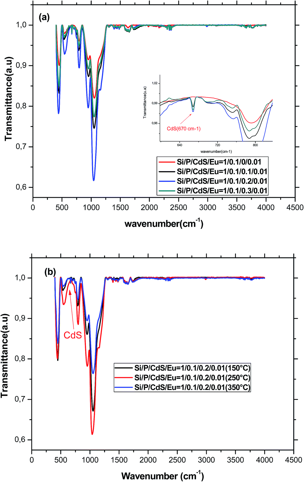 | ||
| Fig. 1 (a) FTIR spectra of glasses containing different amount of CdS nanoparticles and annealed at 250 °C. (b) FTIR spectra of glasses having the same starting composition and annealed at different temperatures. | ||
Before trying to assign the different bands seen in the FTIR spectra, it is noteworthy to signal the discrepancy observed in the available literature, which may be due to the interference between the bands associated to the different species existing in the glass structure. Therefore, one must be cautious especially when bands may belong either to silicate or phosphate groups. We can however assign without ambiguity the band at about 470 cm−1 to the out-of-plane rocking vibration of the bridging oxygen (BO) where the oxygen atom moves perpendicular to the Si–O–Si plane.19 The presence of this band evidences the formation of three dimensional silicate network in the glass. Similarly, the band around 760 cm−1 is due to the symmetric stretching motion of oxygen atoms parallel to Si–O–Si bonds. This band can be also assigned to symmetrical stretching vibrations of Si–O–P and P–O–P bridges, which are very weak since their formation is statistically less likely than Si–O–Si because of the low P2O5 concentration in this glass. The presence of phosphate in the glass structure is also evidenced by the band located at 546 cm−1 characteristic for the bending O–P–O vibrations of crystalline phosphate.20,21 The overlapping of these bands provide evidences for the formation of the glass skeleton by the condensation reaction and indicates that these glasses are formed as homogeneous and chemical, rather than mechanical. The shoulder at about 1200 cm−1 is attributed to the transverse optical mode of the asymmetric stretching of Si–O–Si bonds of SiO2.22 The band at 1600 cm−1 is attributed to the bending vibration of adsorbed water H2O, whereas the broad band in the range 3400–3700 cm−1 is due to an overlap of OH stretching vibrations of both molecular water (3440 cm−1) and hydrogen bonded Si–OH or P–OH groups (3650 cm−1).23,24 However, these bands are relatively weak, which means that water has no substantial effect on the structure and the optical properties of the glass. The spectra show also a peak in the range 2340–2360 cm−1, which confirms the presence of –SH groups. These groups can bind with cadmium and forms CdS nanoparticles. Moreover, the inclusion of CdS nanoparticles was confirmed by the presence of the characteristic Cd–S stretching vibrational peak at 670 cm−1.25,26 With increasing the concentration of CdS nanoparticles, the bands related to the glass structure become more and more intense before decreasing when the doping level exceeds 0.2%. This may be indicative of the lowering of network dimensionality by breaking of Si–O–Si bridges within the structure of glass. Indeed, it is known that CdS nanoparticles enter the glass as a network modifier increasing thus the concentration of non-bridging oxygen and weakening the Si–O–Si bonds.27 We can also note an increase of the bands involving OH groups indicating that CdS nanoparticles, which grow inside pores, entrap water and inhibit its evaporation.
The bands in the FTIR spectrum remain at the same positions but their intensities increases until annealing temperature reaches 250 °C. After that, the intensities decrease again. The remarkably increase is due to the condensation of silanol (Si–OH) and phosphanol (P–OH) groups to form Si–O–Si and P–O–P. At annealing temperature equal to 350 °C, all the observed bands decreased. Particularly, the decrease of the band at 546 cm−1 associated to the O–P–O bridges is more pronounced indicating the insertion of the small amount of phosphorus into the three dimensions silicate structure and the formation of a mixed silicate–phosphate network.
2. XRD and TEM characterisation
As indicated in Fig. 2, the XRD diffraction patterns of CdS samples displayed a broad peak characteristic of the amorphous nature of the glass matrix together with four diffraction peaks at 2θ = 38.44°, 44.66°, 64.70° and 78.00°. By using XRD database (JCPDS 80-0019), these peaks were assigned to (102), (110), (203), and (105) planes of CdS nanoparticles with hexagonal crystal structure. The nonappearance of the (100), (002), (101) planes in the diffraction patterns of the different samples may be due to their overlap with the amorphous hump. Additionally, the change of the relative intensities of the diffraction peaks as shown in Fig. 2 means that the direction of growth and the morphology of the nanoparticles of the formed CdS nanoparticles depend on the initial composition and the annealing temperature. We note however, that the narrower peaks reveal good crystallization of the nanoparticles was obtained for an annealing temperature of 250 °C and a molar CdS concentration of 0.02. This may be due to the initial porosity of the glass, which controls the growth of the nanoparticles and commands their size. Additionally, when annealing temperature exceeds 250 °C, it may happen an oxidation or the melt of CdS nanoparticles, which becomes more amorphous. Beyond melting point, CdS nanoparticles rearrange and finally provide less ordered structure or decompose. Indeed, depending on their size, CdS nanoparticles have a melting point much lower than the corresponding bulk material. The average CdS crystallite size was estimated by using the Scherrer's equation:28where λ = 1.54060 Å (CuKα) and β is the full width at half maximum intensity of the peak (in Rad). For the same CdS molar concentration, increasing annealing temperature from 150 °C to 350 °C, results in a decrease of the average crystallite diameter from 24 to 21 nm. At a constant annealing temperature, the crystallite size passes from 10 to 23 nm before decreasing to 20 nm for the highest CdS concentration.
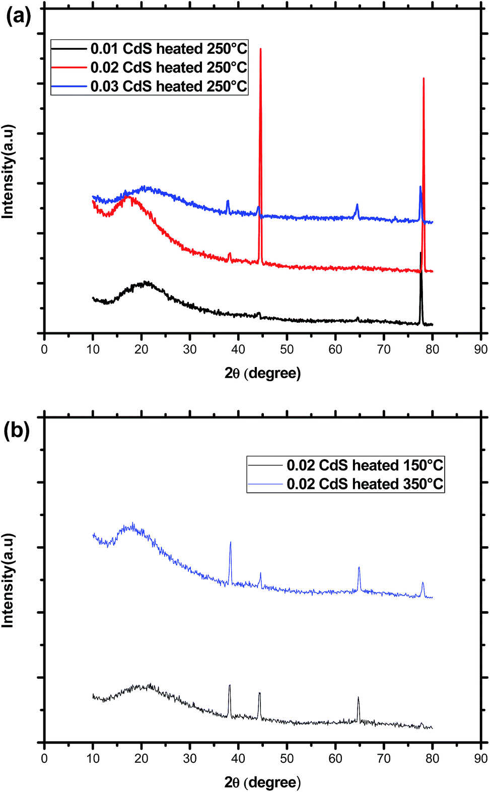 | ||
| Fig. 2 (a) XRD patterns of sol–gel glass samples doped with different CdS concentrations and annealed at the same temperature (250 °C). (b) XRD patterns of sol–gel glass samples having the same CdS concentration and annealed at different temperatures (150 °C and 350 °C). | ||
TEM image presented in Fig. 3 indicates the presence of small spherical nanoparticles having a diameter ranging from 2 to 5 nm together with large domain with a diameter of nearly 24 nm dispersed in the homogeneous amorphous matrix. This later value is comparable to the crystallite size deduced from XRD study, which means that diffractions peaks originate majorly from particles having the greatest size. Indeed, it was reported that for high CdS concentration, micro-pores collapse resulting in CdS domains growth whereas meso-pores reduce their size to give much narrower distribution.29
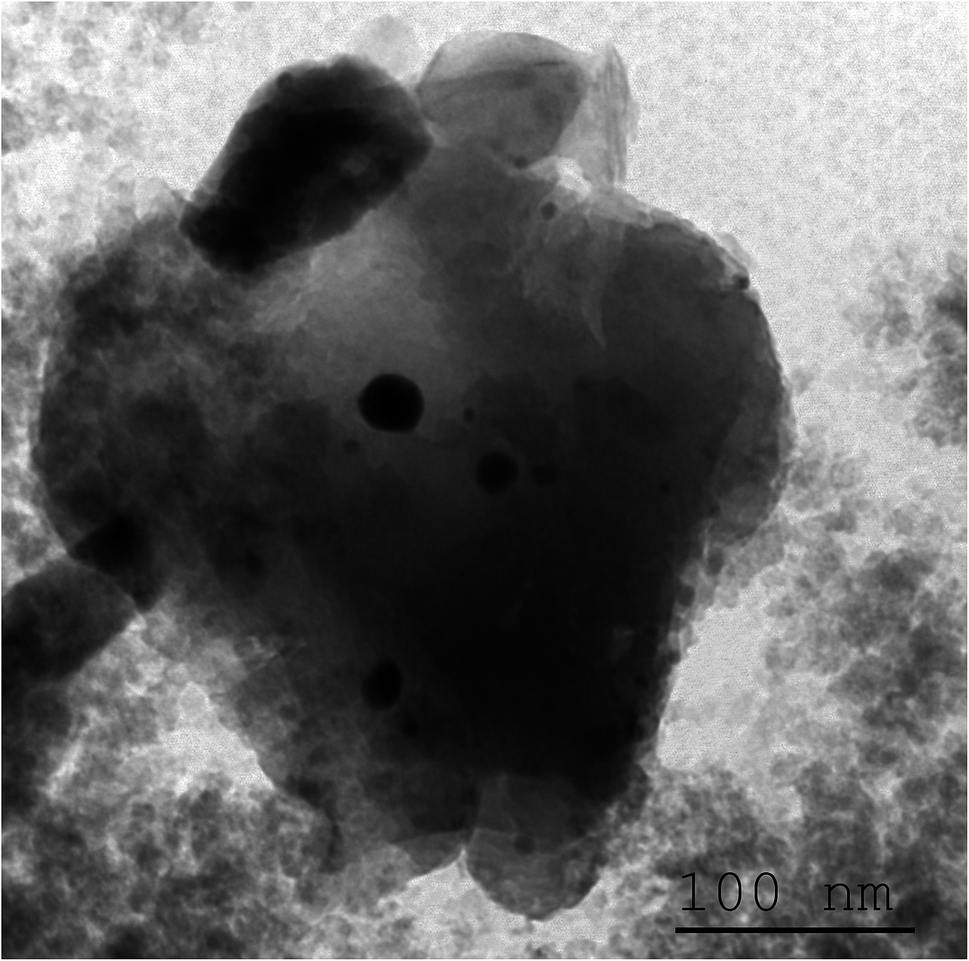 | ||
| Fig. 3 TEM image of a glass sample annealed at 250 °C showing small nanoparticles together with large domains of CdS crystalline phase. | ||
3. Optical absorption
According to Brus,30 the particle size of a spherical semiconductor quantum dot is related to the optical bandgap throw the following relation:
 | (1) |
The band gap energy of the semiconductor nanoparticles can be estimated from the first minimum of the second derivative of the optical absorption spectrum (Fig. 4), which locate the center of the absorption peak corresponding to the lowest energy transition between the ground hole (1Sh) and electron (1Se) levels of quantum dots.33 The optical gap obtained for the different sample was nearly equal to 3.53 eV regardless the heat-treatment condition or CdS concentration. As compared to bulk CdS, this value is largely greater indicating a strong confinement of the charge carriers inside the nanocrystals. Using the estimated value of Eg(R), the particles diameter was estimated to be equal to 2.42 nm for the different samples. Two arguments can be advanced to explain this behavior. Firstly, the precursors for CdS precipitation in the starting composition may be too small to give large nanocrystals. Secondly, the growth of these nanocrystals takes place within the pores, where they are protected against further growth even for higher treatment-temperatures or great amount of semiconductor reagent in the starting composition.34 In the other hand, the microstructure of the final gel depends on various parameters such as the PH and the chemical composition. Since the different samples was prepared in the same conditions, they will exhibit pores with the same size.35,36 It can be noted however, that the size estimated from optical absorption measurements is much smaller compared to that observed from TEM and XRD studies. This discrepancy may be due to a major contribution to the optical absorption of the smallest nanoparticles, which have the large volume fraction as revealed by TEM image. Additionally, small particles do not diffract well owing to their limited size and the XRD patterns is due to larger CdS particles, which have much more reflection planes.
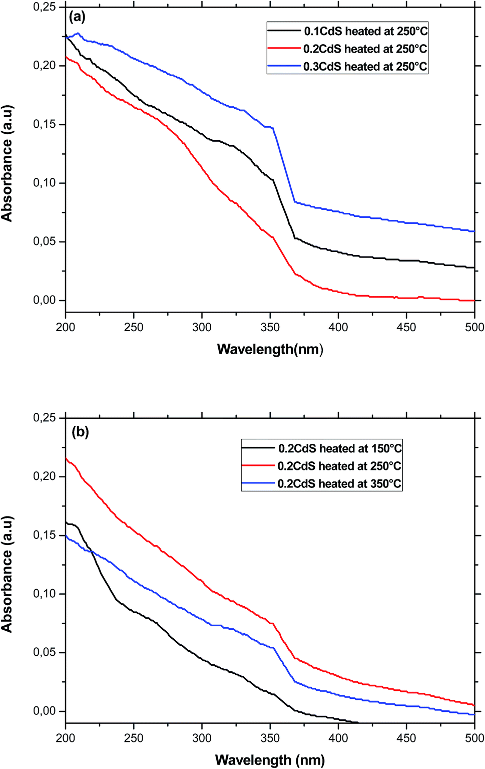 | ||
| Fig. 4 (a) Absorption spectra of glasses containing different amount of CdS nanoparticles and annealed at 250 °C. (b) Optical spectra of glasses having the same starting composition and annealed at different temperatures. | ||
4. Photoluminescence
Under an excitation at 375 nm, the PL spectra of the sample doped only with CdS exhibits a narrow emission band in the UV region centered at 406 nm, which is Stokes-shifted from absorption onset of CdS nanocrystals together with a weak and large band peaking at 647 nm. These two emissions are ascribed respectively to shallow traps (ST) and deep traps (DT) states in the bandgap of CdS nanocrystals. However, for samples containing both CdS and Eu3+ ions, the spectra show the tail of a narrow peak attributed to shallow traps together with a large band extending in the range of 450 to 600 nm and a weak structure in the low energy side (Fig. 5). Indeed, it is well established that for nanosized CdS particles, the emission involves surface states due to the presence of native defects, such as cadmium interstitials and vacancies as well as sulfur interstitials and vacancies.38 The ratio between DT and ST emission varies depending on the amount of defects inside CdS nanoparticles or on their surface. Therefore, we can conclude by comparing the spectra of Fig. 5, that Eu3+, codoping generates novel trap states within the gap of CdS nanoparticles, which results in the intense emission in the range between 450 and 600 nm. Indeed, Eu3+ ions may be inserted inside or at the surface of CdS nanoparticles by substituting cadmium cation. Additionally, the small blue shift in the ST emission indicates that Eu3+ codoping affect slightly the processes of nucleation and growth of CdS nanocrystals within the silica matrix.
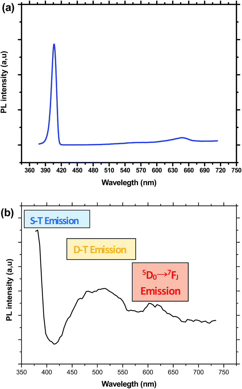 | ||
| Fig. 5 (a) Emission spectrum of CdS doped glass obtained under an excitation at 375 nm. (b) Emission spectrum of CdS/Eu3+ doped glass obtained under an excitation at 375 nm. | ||
The DT band overlap with most of the excitation lines of Eu3+, which may be favorable for an efficient CdS → Eu3+ energy transfer. Co-doping with Eu3+ ions partially quenches this broad emission band and additionally produces the structure in the low energy side, which is assigned to transitions inside the 4f shell of europium ions.
When the excitation wavelength is turned to 355 nm, each of the PL spectra displays only five emission peaks at about 579, 592, 611, 651, and 700 nm, which are associated to the transitions from 5D0 to 7FJ (J = 0, 1, 2, 3, 4), respectively (Fig. 6). Since the lifetime of CdS fluorescence is so much shorter than that of Europium emission, CdS emission is not seen in all the PL spectra of the co-doped samples. As compared to the reference sample doped only with Eu3+ ions, we can see a drastic improvement of the Eu3+ emission with the introduction of CdS nanoparticles in the glass matrix. The enhancement of the emission intensity of europium ions may be accomplished via profound modification of the glass network around rare earth ions and/or efficient energy transfer from CdS to Eu3+ ions.39 Indeed, semiconductor nanoparticles, which act as network modifier, may provoke a deep structural modification of the coordination sphere of the rare earth element. It also contributes to distort the local symmetry around the rare earth ions and therefore promotes an enhancement of the transition rates. In fact, the 5D0 → 7F1 orange emission around 592 nm is allowed by magnetic dipole (MD) interaction, whereas the band at 611 nm relative to 5D0 → 7F2 transition is electric dipole (ED) in nature. Therefore, 5D0 → 7F1 transition is relatively insensitive to the local symmetry, while 5D0 → 7F2 transition is particularly dependent on the local site symmetry around the rare earth ion and the nature of the bonding with its neighbours. When the Eu3+ ions are situated at low-symmetry sites, the forced dipole transition has a larger probability than that of the magnetic transition. Accordingly, the intensity ratio R of ED transition with respect to MD transition gives a measure of the distortion from the inversion symmetry at the Eu3+ site. A greater ratio corresponds to a more distorted or asymmetric local environment. Moreover, R is also related to the covalency of Eu–O chemical bonding. Therefore, this ratio is dependent on the glass host composition, activator concentration and heat-treatment, and it is widely used to investigate the local environment of the rare element. In the case of the present study, the relative intensity of the 5D0 → 7F2 and 5D0 → 7F1 transitions was obtained by measuring the area under the corresponding emission bands. The obtained values for the different concentration are between 2.4 and 3.1, which are characteristic for Eu3+ ions in highly asymmetric sites. However, these values are lower than those estimated for sol–gel silica glasses.40 Similar to the effect of aluminium,41 the addition of phosphorous in a convenient concentration, makes the glass structure less rigid, the local structure less distorted, and Eu3+ ions tend to occupy more symmetric sites with a more homogeneous distribution. Since no quenching of the emission was observed for the used CdS concentrations, we believe that silicophosphate glass is more suitable to disperse great amount of either CdS or Eu3+ ions than only one-component silica glasses.39 This may be due to the role of phosphorus, which is known to preclude rare earth clustering. Moreover, CdS nanoparticles act as network modifier producing non-bridging CdS–O groups, which can coordinate with europium ions. As a result, the Eu–Eu interaction is diminished and the europium emission is increased. The presence of CdS nanocrystallites may be also responsible for an increase of both the covalency and the polarization of the local vicinities of the Eu3+ ions, which can be affected by reaction with sulfur.42 The increase of the asymmetry factor R for the higher concentration of CdS is an indication for an important distortion in the glass network due to the filling of more pores by semiconductor nanoparticles.
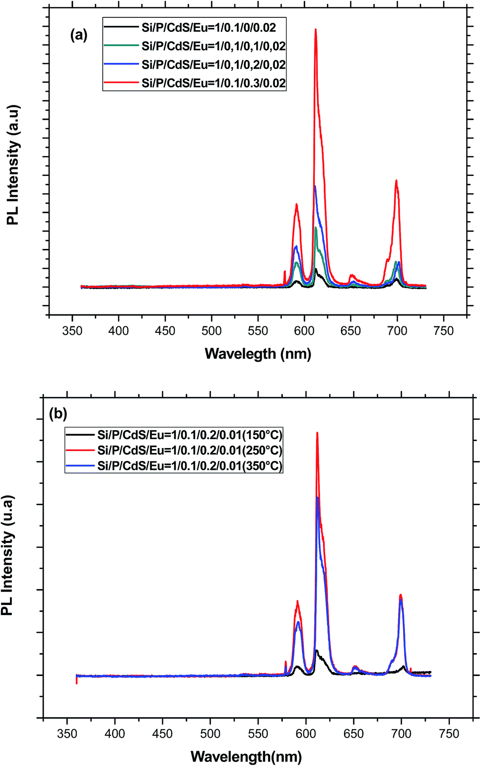 | ||
| Fig. 6 (a) PL spectra recorded under an excitation at 355 nm for glasses containing different amounts of CdS nanoparticles and annealed at 250 °C. (b) PL spectra recorded under an excitation at 355 nm for glasses having the same starting composition and annealed at different temperatures. | ||
In the other hand, the increase of the Eu3+ emission intensity may be due to an energy transfer (ET) between the CdS nanoparticles and Eu3+ ions. So that, this process occurs only when the distance between CdS nanoparticles and Eu3+ ions becomes sufficiently short. However, owing to the fast radiative and non-radiative decay of excitons in CdS, direct energy transfer from semiconductor nanoparticles to Eu3+ ions is physically impossible. Indeed, for achieving efficient energy transfer, the emission spectrum of the nanoparticles has to spectrally overlap an absorption band of the rare-earth ions. This is not the case for the exciton energy level of CdS nanoparticles. However, efficient energy transfer to Eu3+ ion may be achieved when defect states at the semiconductor nanocrystals surface are abundant. As it is well known, these defects give rise to trap levels within the gap of the semiconductor nanoparticles, and their corresponding emission overlap well with the absorption bands of Eu3+. When excitation light is absorbed mostly by CdS nanocrystals, it generates electron–hole pairs. Photo-generated electrons will be first trapped at these levels before interacting with the Eu3+ ions located close to the surface of CdS. Then, the electron trapped at the surface recombines with a valence band free hole or trapped hole at the nanocrystal surface before transition energy being non-radiatively transferred to the Eu3+ ions. The involved processes in this energy transfer are schematically represented in Fig. 7. Increasing CdS concentration will reduce the distance between semiconductor quantum dots and rare earth ions enhancing thus the energy transfer rate between CdS and Eu3+. However, when these species are spatially close, a diminution of the total emission and lifetime values is usually observed, which is assigned to back energy transfer (BET) from the Eu3+ ions to CdS nanoparticles.39 Further, the fact that the europium emission did not appear clearly in the PL spectra recorded under an excitation wavelength of 375 nm as they were obtained under 355 nm excitation, may be connected to the effect of energy transfer in the emission process of Eu3+ ions. Indeed, when using 355 nm wavelength, which is confidently matched with the bandgap energy of the nanoparticles, the number of excited CdS nanoparticles, which contribute to energy transfer to Eu3+ is greater than that reached when 375 nm is used. Therefore, the emission of Eu3+ ions will be so weak in the latter case. Similar behavior was observed in SiO2 gel doped with Eu3+ and ZnO nanocrystals.43 Additionally, the fact that no luminescence from CdS nanocrystals was observed under 355 nm excitation wavelength indicates that energy transfer from a nanocrystal to Eu3+ is so fast. Indeed, when CdS are coupled to Eu3+, any generated exciton will immediately recombine non-radiatively by exciting Eu3+ ions.44
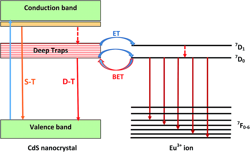 | ||
| Fig. 7 Energy levels diagram showing the different process involved in the emission of CdS/Eu3+ doped glasses. | ||
To clarify the effect of annealing on the local environment around Eu3+ ions, we have estimated again the ratio R for different annealing temperatures. As shown in Table 1, this ratio increases as long as the annealing temperature does not exceed 250 °C. Above this temperature, R remains almost constant, which could be due to a rearrangement of the network and an increase of the symmetry around rare earth ions.45
(a) The decay of CdS emission. As an example, Fig. 8 shows the decay curves measured at two different emission wavelengths of CdS nanoparticles under an excitation wavelength of 375 nm. All the obtained curves are nearly exponential. However, the time constant for the emission at 396 nm is equal to 0.98 ns for the sample doped with CdS only and it is nearly constant for the two lower CdS concentrations and equal to 0.88 ns. As it is expected, this time constant is shorter than that estimated for the defect emission at 550 nm which is almost constant (∼2.25 ns) indicating that these defects are of the same origin.
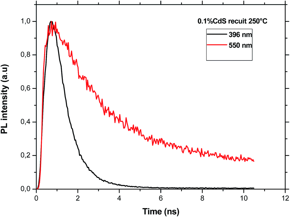 | ||
| Fig. 8 PL decay curves recorded at two wavelengths under an excitation at 375 nm. | ||
As it was mentioned above, energy transfer takes place only when a significant overlap exists between the emission spectra of a sensitizer or energy donor (here CdS) and the absorption spectra of an energy acceptor (here Eu3+). Additionally, the efficiency of this transfer depends strongly on the distance r between the two species, and is given by:46
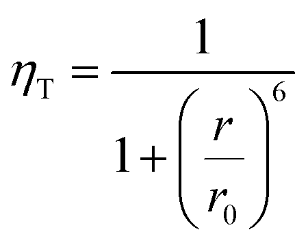 | (2) |
According to Forster model, the energy transfer efficiency of a donor–acceptor pair can be measured experimentally using either fluorescence intensities or lifetimes of the donor in the presence and in the absence of acceptors according to the following equations:47,48
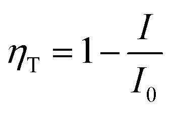 | (3a) |
 | (3b) |
These results indicates that it is not necessary to incorporate a great amount of semiconductor nanoparticles to enhance the emission of Eu3+. Instead of that, one must optimize the quantity of CdS to be incorporated in the glass in order to simultaneously improve the emission of Eu3+ and avoid back energy transfer.
(b) The decay of Eu3+ emission. To get more insight on the emission process of Eu3+ ions in presence of CdS nanoparticles, the decay curves were measured in the timescale of millisecond rather than nanoseconds at the wavelength 611 nm (Fig. 9). Although the PL decay is not exponential, we have used the following formula to estimate the average PL lifetimes for all the samples:
 | (4) |
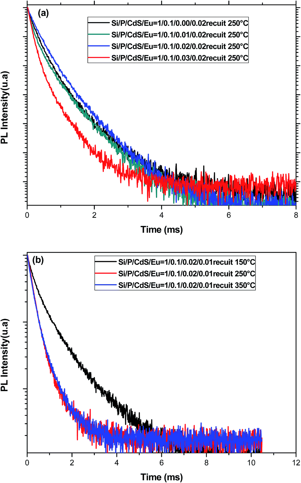 | ||
| Fig. 9 (a) PL decay curves for glasses containing different amounts of CdS nanoparticles and annealed at 250 °C recorded at 611 nm under an excitation at 355 nm. (b) PL decay for glasses having the same starting composition and annealed at different temperatures recorded at 611 nm under an excitation at 355 nm. | ||
However, when the concentration of CdS nanoparticles exceeds a threshold, their presence becomes nocuous for the emission of Eu3+ ions since they will be very close favoring BET. Moreover, when CdS are present in a great fraction, they may prevent efficient elimination of adsorbed water in the gel pores. These two effects are mainly the origin of the lifetime reduction for higher CdS content. On the other hand, through annealing treatment, the glass structure becomes more compact reducing thus distances between emitting spices and favoring the non-desired europium aggregation and BET that act as quenchers for the luminescence of Eu3+. This may explain the decrease of the lifetime of the 5D0 level with the annealing temperature. Additionally, the decay curves are also non exponential, and they may be fitted by two exponential functions which are associated to two sets of europium sites usually observed in glasses with more than one constituent.50 In the case of the present study, europium ions may be located in either a silica rich or a phosphorus rich phase.51
It is noteworthy to say that no correlation between the emission enhancement and the lifetime evolution of 2D1 level of Eu3+ ions was observed. This indicates the complexity of the emission processes involved in the emission of these ions. Indeed, although energy transfer from CdS increases the population of the emitting levels of Eu3+, it does not influence their emission probability to the ground level.52
IV. Conclusion
We have investigated the effect of CdS nanocrystals on the emission of Eu3+ ions embedded in a silicophosphate glass prepared by the sol gel method. From this study, it was shown that Eu3+ emission is significantly dependent on concentration of CdS nanoparticles and annealing temperature. Additionally, it was evidenced via photoluminescence measurement that a fast CdS → Eu3+ energy transfer and/or structural distortions around the rare earth ions induce the enhancement of the emission of Eu3+ ions. Further, it was revealed the presence of back energy transfer, which takes place when the concentration of CdS nanoparticles or the heat-treatment temperature exceeds a threshold. Thus, to get the desired emission improvement, it is necessary to optimize either the CdS amount or the annealing temperature.Acknowledgements
The authors are grateful to Pr K. Khirouni from Faculté des Sciences de Gabes (Tunisia) for optical absorption measurements and A. Kouki from Faculté des Sciences de Bizerte (Tunisia) for providing TEM images.References
- T. Adachi and S. Sakka, J. Mater. Sci., 1987, 22, 4407–4410 CrossRef CAS.
- K. Kajihara, Journal of Asian Ceramic Societies, 2013, 1, 121–133 CrossRef.
- K. Driesen, V. K. Tikhomirov and C. Görller-Walrand, J. Appl. Phys., 2007, 102, 024312–024316 CrossRef.
- C. E. Secu, R. F. Negrea and M. Secu, Opt. Mater., 2013, 2456–2460 CrossRef CAS.
- K. Binnemans, Chem. Rev., 2009, 109, 4283–4374 CrossRef CAS PubMed.
- G. Gao and L. Wondraczek, J. Mater. Chem. C, 2014, 2, 691–695 RSC.
- K. Binnemans, Coord. Chem. Rev., 2015, 295, 1–45 CrossRef CAS.
- G. C. Righini and M. Ferrari, Riv. Nuovo Cimento, 2005, 28, 1–53 CAS.
- B. C. Joshi, J. Non-Cryst. Solids, 1995, 180, 217–220 CrossRef CAS.
- L. Su, N. Qin, T. Sa and D. Bao, Opt. Express, 2013, 21, 29425–29434 CrossRef PubMed.
- Y. Dwivedi, S. N. Thakur and S. B. Rai, Appl. Phys. B, 2007, 89, 45–51 CrossRef CAS.
- C. H. Huang and T. M. Chen, Opt. Express, 2010, 18, 5089–5099 CrossRef CAS PubMed.
- G. Ehrhart, B. Capoen, O. Robbe, F. Beclin, Ph. Boy, S. Turrell and M. Bouazaou, Opt. Mater., 2008, 30, 1595–1602 CrossRef CAS.
- S. Suresh, Appl. Nanosci., 2014, 4, 325–329 CrossRef CAS.
- M. A. Correa-Duarte, M. Giersig and L. M. Liz-Marzán, Chem. Phys. Lett., 1998, 286, 497–501 CrossRef CAS.
- N. Thanha and L. Green, Nano Today, 2010, 5, 213–230 CrossRef.
- K. Kajihara, S. Kuwatani and K. Kanamura, Appl. Phys. Express, 2011, 5, 012601–012605 CrossRef.
- N. Bel Haj Mohamed, M. Haouari, R. Ebdelli, Z. Zaaboub, M. M. Habchi, F. Hassen, H. Maaref and H. Ben Ouada, Phys. E, 2015, 69145–69152 Search PubMed.
- P. Innocenzi, J. Non-Cryst. Solids, 2003, 316, 309–319 CrossRef CAS.
- A. Vulpoi, L. Baia, S. Simon and V. Simon, Mater. Sci. Eng., C, 2012, 32, 178–183 CrossRef CAS.
- M. Sitarz, K. Bulat, A. Wajda and M. Szumera, J. Therm. Anal. Calorim., 2013, 113, 1363–1368 CrossRef CAS.
- F. Orgaz and H. Rawson, J. Non-Cryst. Solids, 1986, 82, 57–68 CrossRef CAS.
- K. M. Davis and M. Tomozawa, J. Non-Cryst. Solids, 1996, 201, 177–198 CrossRef CAS.
- A. Aronne, M. Turco, G. Bagnasco, P. Pernice, M. Di Serio, N. J. Clayden, E. Marenna and E. Fanelli, Chem. Mater., 2005, 17, 2081–2090 CrossRef CAS.
- N. Rajeswari Yogamalar, K. Sadhanandam, A. Chandra Bose and R. Jayavel, RSC Adv., 2015, 5, 16856–16869 RSC.
- K. Ravichandran and P. Philominathan, Sol. Energy, 2008, 82, 1062–1066 CrossRef CAS.
- T. Martin and H. Schaber, Spectrochim. Acta, Part A, 1982, 38, 655–660 CrossRef.
- S. Rai, L. Bokatial and P. J. Dihingia, J. Lumin., 2011, 131, 978–983 CrossRef CAS.
- L. Esquivias, R. Litran, J. A. Rodriguez-Ortega, E. Blanco, M. Ramirez-Del-Solar and N. De La Rosa-Fox, J. Sol-Gel Sci. Technol., 1998, 11, 217–227 CrossRef CAS.
- L. E. Brus, J. Chem. Phys., 1984, 80, 4403–4409 CrossRef CAS.
- G. Ghosh, M. Kanti Naskar, A. Patra and M. Chatterjee, Opt. Mater., 2006, 28, 1047–1053 CrossRef CAS.
- K. Sulabha and K. Kulkarni, Nanotechnology: Principles and Practices, Springer, 2014 Search PubMed.
- A. Goldstein, Handbook of Nanophase Materials, CRC Press, 1997 Search PubMed.
- M. Wark, H. Wellmann and J. Rathousky, Thin Solid Films, 2004, 458, 20–25 CrossRef CAS.
- J. D. Mackenzie and E. P. Bescher, Acc. Chem. Res., 2007, 40, 810–818 CrossRef CAS PubMed.
- M. Guglielmi, A. Martucci, E. Menegazzo, G. C. Righini and A. N. D. S. Pelli, J. Sol-Gel Sci. Technol., 1997, 8, 1017–1021 CAS.
- V. Mangalam, K. Pita and C. Couteau, Nanoscale Res. Lett., 2016, 11, 1931–7573 CrossRef PubMed.
- P. K. Narayanam, P. Sonia, P. Mohanta, R. S. Srinivasa, S. S. Talwar and S. S. Major, Mater. Chem. Phys., 2013, 139, 196–209 CrossRef CAS.
- L. Bokatial and S. Rai, J. Fluoresc., 2012, 22, 505–510 CrossRef CAS PubMed.
- B. Julian, J. Planelles, E. Cordoncillo, P. Escribano, P. Aschehoug, C. Sanchez, B. Viana and F. Pelle, J. Mater. Chem., 2006, 16, 4612–4618 RSC.
- G. Alombert-Goget, N. Gaumer, J. Obriot, A. Rammal, S. Chaussedent, A. Monteil, H. Portales, A. Chiasera and M. Ferrari, J. Non-Cryst. Solids, 2005, 351, 1754–1758 CrossRef CAS.
- R. Reisfeld, M. Zelner, T. Saraidarov and H. Minti, Advances in Energy Transfer Processes, World Scientific, 2001 Search PubMed.
- V. Mangalam, K. Pita and C. Couteau, Nanoscale Res. Lett., 2016, 11, 9, DOI:10.1186/s11671-016-1282-3.
- P. G. Kik and A. Polman, Mater. Sci. Eng., B, 2001, 81, 3–8 CrossRef.
- G. Gao, N. Da, S. Reibstein and L. Wondraczek, Opt. Express, 2010, 18, 575–583 CrossRef PubMed.
- T. Förster, Discuss. Faraday Soc., 1959, 27, 7–17 RSC.
- J. R. Lakowicz, Principles of Fluorescence Spectroscopy, Springer, New York, 3rd edn, 2006 Search PubMed.
- B. Valeur, Molecular Fluorescence: Principles and Applications, Wiley-VCH, Weinheim, 2nd edn, 2012 Search PubMed.
- A. Monteil, S. Chaussedent, G. Alombert-Goget, N. Gaumer, J. Obriot, S. J. L. Ribeiro, Y. Messaddeq, A. Chiasera and M. Ferrar, J. Non-Cryst. Solids, 2004, 348, 44–50 CrossRef CAS.
- G. Pucker, K. Gatterer, H. P. Fritzer, M. Bettinelli and M. Ferrari, Phys. Rev. B: Condens. Matter Mater. Phys., 1996, 53, 6225–6234 CrossRef CAS.
- F. Ben Slimen, M. Haouari, H. Ben Ouada, D. Guichaoua, P. Raso, X. Bidault, J. Turlier, N. Gaumer and S. Chaussedent, Opt. Mater., 2017, 64, 479–488 CrossRef CAS.
- S. Sadhu, P. S. Chowdhury and A. Patra, J. Lumin., 2007, 126, 387–392 CrossRef CAS.
| This journal is © The Royal Society of Chemistry 2017 |