DOI:
10.1039/C6RA27280K
(Paper)
RSC Adv., 2017,
7, 14544-14551
Fabrication of ultra-smooth and oxide-free molecule-ferromagnetic metal interfaces for applications in molecular electronics under ordinary laboratory conditions†
Received
24th November 2016
, Accepted 24th February 2017
First published on 6th March 2017
Abstract
Self-assembled monolayers of alkanethiolates on ferromagnetic metal surfaces have potential applications in molecular spintronics, but the fabrication of such structures is complicated by unwanted oxidation of the ferromagnetic metal. This paper describes the fabrication of ultra-smooth oxide-free Ni surfaces via template-stripping which are protected by SAMs of S(CH2)n−1CH3 that are stable for 1 day in ambient environment. Our method does not require ultra-high vacuum conditions, glove-box techniques, or (redox) cleaning of the Ni surface, but can be readily applied under ordinary laboratory conditions. Passivation of the Si/SiO2 template with a layer of FOTS (1H,1H,2H,2H-perfluorooctyltrichlorosilane) reduced the Ni-template interaction sufficiently enabling successful template-stripping. The NiTS–SAM interfaces were characterized by X-ray photoelectron spectroscopy (XPS) and atomic force microscopy (AFM). We found that the surfaces were ultra-flat with a root mean square surface roughness of 0.15 ± 0.05 nm over 1.0 × 1.0 μm2 and that they were stable against oxidation for 1 day in air at room temperature. These SAMs on Ni were incorporated in SAM-based tunneling junctions of the form NiTS–SCn//GaOx/EGaIn to study the tunneling rate across the SAMs. The tunneling rate is highly sensitive to defects in the SAMs or the presences of oxides. We found that the charge transport properties across these junctions were indistinguishable from those junctions with formed on AuTS and AgTS substrates from which we conclude that our method yields high quality NiTS–SAM interfaces suitable for applications in molecular electronics.
Introduction
Self-assembled monolayers (SAMs) of thiol-functionalized molecules on ferromagnetic metal (FM) surfaces are interesting for possible applications in molecular,1–5 and biomolecular-spintronics.6–8 Such studies are challenging because the formation of metal oxides has to be minimized to ensure efficient spin-dependent charge transport1–4 and thus there is a need to have easy access to high quality, oxide free, and defect free FM electrodes. Template-stripping (TS) is a well-known technique to generate ultra-smooth and clean metal surfaces on demand.9–12 Often, a clean and ultra-smooth silicon (Si) surface with its native layer of SiO2 is used as the template onto which a thin metal film is deposited. Next, a support, e.g., a glass surface, is glued against the metal and the support/glue/metal stack is stripped off the template to expose the metal surface that had been in contact with the template when needed. Since the metal surface was in contact with the template it is protected from the ambient environment and the template serves in this regard as a protective barrier which avoids contamination and oxidation of the metal surface. Although this method works well for inert metals such as Ag, Au, Pd, or Pt, reactive metals tend to interact too strongly with the template preventing successful template-stripping.
Here, we report a method to fabricate ultra-smooth and oxide free template-stripped nickel (NiTS) surfaces that can be obtained under ordinary laboratory conditions. This method makes it possible to strip off Ni from the Si/SiO2 template via passivation of the template with a monolayer with a low surface energy. We characterized the SAM and NiTS surfaces with X-ray photoelectron spectroscopy (XPS) to confirm successful fabrication of oxide free FM-SAM interfaces. Our method does not rely on any ultra-high vacuum (UHV) environments and/or electrochemical reduction/cleaning processes.13–16 Prior to template-stripping, the Ni substrates can be stored in ambient conditions for a period of time of 4–6 months. To demonstrate their usefulness, we prepared good quality molecular tunneling junctions of the form NiTS–SCn//GaOx/EGaIn, where, the SCn is a SAM of n-alkanethiolates of the form of S(CH2)n−1CH3 with n = 10–18. The GaOx/EGaIn top-electrodes have been well-characterized and EGaIn stands for eutectic mixture of Ga and In (mp = 15.7 °C) which has a self-limiting surface layer of conductive, 0.7 nm thick GaOx (predominantly consisting of Ga2O3).17,18 The electrical properties of the tunnel junctions are given by eqn (1), in which tunneling processes are characterized by the exponential decay of the current density J (in A cm−2) as a function of the tunneling distance d (in nm).
where the
β (nC
−1) is the tunneling decay coefficient and
J0 (A cm
−2) is the pre-exponential factor for a predefined applied bias.
19–22 The results show that the SAMs form good quality tunneling barriers on Ni
TS with
β = 1.01 ± 0.03 nC
−1 and log
10|
J0| = 2.3 ± 0.2 A cm
−2; these values are well within the range of consensus values.
20–23 These junctions also show good yields (>90%) in non-shorting junctions and high precision of data with log-standard deviations of 0.3–0.5 similar to junctions with Ag or Au bottom electrodes.
19–23
The self-assembly of alkyl/aryl thiols on FM surfaces, such as nickel (Ni),6,13–16,24 cobalt (Co),14,15,24,25 and iron (Fe),14 are challenging due to the presence of the native oxide which hampers the formation of the metal-thiolate bonds. Therefore, SAMs are immobilized on FM surfaces via this native oxide layer using carboxylate, phosphonate, or silane, anchoring groups.26–29 The presence of a native oxide layer, however, often forms an antiferromagnetic (AFM) passivation layer which hinders the reorientation of ferromagnetic moment of the FM layer by exchange coupling lowering the performance of, for example, spin valves.30–32 Thus, to develop fabrication methods to obtain oxide free molecular-FM interfaces are important for molecular spintronics.
Fabrication methods based on highly controlled ultra-high vacuum (UHV) environments or in situ electrochemical control are available.4,5,33–36 Most electrochemical techniques are based on a two-step procedure involving removal of the native oxide by electrochemical reduction, followed by immediate substrate immersion in alkanethiol containing ethanolic solutions. During transfer of the oxide free Ni surface, metal-oxides can form as the substrates are exposed to air. For example, Bengió et al.34 reported the fabrication of n-alkanethiolate SAMs on Ni(111) and polycrystalline Ni surfaces by the electrochemical reduction method in which the electrochemical reduction was performed under either acidic or basic aqueous conditions, while the SAM formation was carried out either in situ or by pulling the substrate through a top layer of neat thiol. Instead of using two separate steps and acidic or basic aqueous electrolyte, Fontanesi et al.35 performed electrochemical removal of the oxide layer with the thiol precursor present in the electrolyte (1![[thin space (1/6-em)]](https://www.rsc.org/images/entities/char_2009.gif) :0.8, ethanol:water) and reported good quality SAMs. Hoertz et al.14 used three different methods for SAM formation on Ni, Co and Fe substrates, (i) glovebox techniques (freshly evaporated metal transfer to a solution of the SAM precursor without exposure to air), (ii) electrochemical reduction inside a glovebox (oxide removal by electrochemical reduction and SAM formation carried out inside the glovebox), and (iii) deposition of metal via direct metal evaporation followed by a brief exposure in air before immersion into a solution with the SAM precursor. The stability of hexadecanethiolate SAM prepared by method (i) and (ii) on FMs was examined by XPS, the sulfur atom oxidized to a S
:0.8, ethanol:water) and reported good quality SAMs. Hoertz et al.14 used three different methods for SAM formation on Ni, Co and Fe substrates, (i) glovebox techniques (freshly evaporated metal transfer to a solution of the SAM precursor without exposure to air), (ii) electrochemical reduction inside a glovebox (oxide removal by electrochemical reduction and SAM formation carried out inside the glovebox), and (iii) deposition of metal via direct metal evaporation followed by a brief exposure in air before immersion into a solution with the SAM precursor. The stability of hexadecanethiolate SAM prepared by method (i) and (ii) on FMs was examined by XPS, the sulfur atom oxidized to a S![[double bond, length as m-dash]](https://www.rsc.org/images/entities/char_e001.gif) O containing species (e.g., sulfonate, sulfinate, sulfone) within 2 hours of exposure to the ambient atmosphere confirmed by the appearance of S 2p peak at ∼169 eV. After five days of exposure the sample contained predominantly oxidized sulfur atoms. The oxidation of Ni surfaces slows down by the presence of SAMs under atmospheric conditions. Hoertz et al.14 reported, alkanethiolate SAM on Ni surface slowed down the formation of the Ni oxide by 1–2 hours using X-ray photoelectron spectroscopy (XPS). As a group, these studies show that storing of FM surfaces is challenging.
O containing species (e.g., sulfonate, sulfinate, sulfone) within 2 hours of exposure to the ambient atmosphere confirmed by the appearance of S 2p peak at ∼169 eV. After five days of exposure the sample contained predominantly oxidized sulfur atoms. The oxidation of Ni surfaces slows down by the presence of SAMs under atmospheric conditions. Hoertz et al.14 reported, alkanethiolate SAM on Ni surface slowed down the formation of the Ni oxide by 1–2 hours using X-ray photoelectron spectroscopy (XPS). As a group, these studies show that storing of FM surfaces is challenging.
Defects in molecular tunneling junctions, such as pinholes, need to be minimized to ensure good quality tunnelling junctions and therefore the surface roughness of the FM surface needs to be kept at a minimum.37–42 Substrates used for preparation of SAMs on Ni by electrochemical methods have typically a root mean square (rms) surface roughness of 2.5 nm over an area of 2 × 2 μm2 which is much higher than the molecular dimensions of the SAMs they support.35 In addition, electrochemical etching increases the rms surface roughness of, for example, Ni and Co, by about ∼40%.14 Although the roughness is usually reported in terms of rms surface roughness, the topography can also be more comprehensively analyzed to include, grain size, width of the grain boundary, presence of pinholes, and whether the grains are located in the same plane or not. The so-called bearing volume (BV, nm3) of the surface topography includes all of these parameters but a BV analysis has been only occasionally reported.11 In this context, TS seems to be an attractive choice to generate FM surfaces because TS produces ultra-flat surfaces, the template provides protection from the atmosphere, and clean metal surfaces are available on demand, and therefore we developed a TS procedure to generate flat and clean Ni surfaces on-demand.
Experimental details
We purchased nickel (Ni) with purity of 99.999% from Super Conductor Material, Inc (USA) and silicon wafers (100, p-type, 500 ± 25 μm) with one side polished from University Wafers (USA). The 1H,1H,2H,2H-perfluorooctyltrichlorosilane (FOTS) and alkanethiols SCn (with n = 10, 12, 14, 16 and 18) were purchased from Sigma-Aldrich with a purity of 98%. We purified the alkanethiols before use as reported previously.39 The n-alkanethiol with n = 6 was purified by distillation under vacuum. The n-alkanethiols with n = 10, 12, 14, 16 and 18 were purified by column chromatography over silica gel with hexane as an eluent and then recrystallised from ethanol under an atmosphere of N2 followed by quick filtration. The gallium–indium eutectic (75.5% Ga and 24.5% In by weight) was purchased from Sigma-Aldrich. The solvents were AR grade.
Fabrication of NiTS substrate
300 nm Ni was evaporated on 1H,1H,2H,2H-perfluorooctyltrichlorosilane (FOTS) functionalized Si(〈100〉) substrate by e-beam evaporation. Before Ni evaporation, the silicon substrate was exposed in FOTS for 30 min at 1 mbar in vacuum desiccators. 300 nm layer of Ni was evaporated at a rate of 0.1 Å s−1 monitored by a quartz crystal thickness controller. We cleaned the glass slides by ultra-sonication in ethanol solution, followed by washing with ethanol, the slides were blown to dryness in a stream on N2 gas. Before we glued the glass on the nickel surfaces with optical adhesive (Norland, No. 61), the glass slides were cleaned by a plasma of air for 5 min at a pressure of 5 mbar. The optical adhesive was cured for 2 hours under UV-light irradiation following previously reported methods.9,39 In order to prevent nickel oxidation template stripping was carried out in a N2 flow hood.
Formation of SAMs on NiTS
The SAMs of alkanethiolates (SCn with n = 10, 12, 14, 16 and 18) were prepared by immersing freshly template-stripped NiTS from the silicon wafer inside the N2 flow hood into 3 mM ethanolic solutions of the alkanethiolate molecule. The SAMs were formed overnight under a N2 atmosphere (Fig. 1) using previously reported methods.43 Then the SAM-modified substrates were rinsed with ethanol and blown to dryness in a stream of N2 gas.
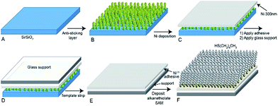 |
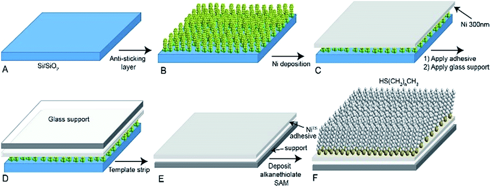
| | Fig. 1 Schematic illustration of the fabrication process of template-stripped Ni (NiTS) coated with a SAM. (A) On a clean Si/SiO2 surface (B) FOTS was deposited followed by (C) deposition of 300 nm Ni. (D) Glass supports were glued on the Ni surface using photocurable optical adhesive. (E) After curing of the adhesive, the metal film around the glass support was cut out using a razor blade. Next, the nickel film, with its glass support, was lifted off to expose an ultra-flat Ni film (inside of a N2 flow hood). (F) The NiTS surface was then immediately transferred into a solution of n-alkanethiolates. | |
Monolayer characterization
The surface chemical composition of the SAMs chemisorbed on NiTS substrate was characterized by XPS using well-established procedures.44 The photoemission spectra were measured using VG ESCA lab-220i XL XPS. The system was equipped with a monochromatic Al Kα X-ray source with a photon energy of 1486.6 eV at 15 kV. The high resolution spectra were collected at a pass energy of 20 eV, with 0.1 eV steps, at a 45° take-off angle. The binding energies were corrected against the C 1s energy of 285.0 eV. The collected XPS high resolution spectra were analysed using XPS Peak fit 4.1 software using Voigt functions (30% Lorentzian and a 70% Gaussian). The background from each spectrum was subtracted using Shirley-type back grounds to remove most of the extrinsic loss structure. The SAM thickness and tilt angle were measured using angle resolved photoelectron spectroscopy (AR-XPS). We used synchrotron-based photoelectron spectroscopy to perform the angle resolved XPS measurements at the SINS (Surface, Interface and Nanostructure Science) beamline of Singapore Synchrotron Light Source (SSLS). The measurements were carried out at room temperature under ultra-high vacuum with a base pressure of 10−10 mbar. We recorded S 2p spectra at different angles of from 0° to 90° to measure surface coverage and tilt angle of SAMs on NiTS surface.
Ultraviolet photoelectron spectroscopy (UPS)
We determined the work function of the NiTS surfaces with and without SAMs with UPS at the SINS beam-line.44 The top of the valence band and work function Φ values were determined by linear extrapolation of the lower binding energy side of the HOMO peak and secondary electron cut-off to the base line.
Atomic force microscopy (AFM)
AFM images were performed in the tapping mode, using Bruker dimension Fastscan (FASTSCAN-A, resonant frequency: 1.4 MHz, force constant: 18 N m−1). We used nanoscope analysis (version 1.4) software to analyse the AFM images.
Junction fabrication and data collection
The junction fabrication and data collection has been reported before.44 Here, we give only a brief description. We used cone-shaped EGaIn tips to approach the Ni–SAM substrates and form a junction with a diameter of 20–30 μm. For each SAM, we fabricated junctions on four to five different samples and collected five to six junctions on each sample. For each junction, we first carried out 5 scans to stabilize the junction and then collected 20 traces (except for shorts), which were all used for data analysis. We defined a short when the value of J exceeded 102 A cm−2 (the compliance value of J of our instrument) during scanning (including the first 5 scans). The yield of non-shorting junctions is defined as the number of stable junctions divided by the total number of junctions. We followed the procedure for statistical analysis of the junction data as reported before.2 Briefly, we plotted the value of log10|J| at a given bias voltage in histograms and fitted Gaussians to these histograms to obtain the log-standard deviation and log-mean of the value of J. We used this procedure for all the applied biases to construct the log-average J(V) curves.
Results and discussion
Fabrication of NiTS substrates
Fig. 1 shows schematically the procedure for the preparation the NiTS substrates and formation of alkanethiolate SAMs of S(CH2)n−1CH3 (in short SCn) on these NiTS surfaces. As a template, we tried to use a Si wafer with its native SiO2 layer (Si/SiO2) or an oxide free Si template. We found that the nickel cannot be stripped off successfully because Ni interacted too strongly with these templates. To be able to peel off the nickel layer from the template, the Ni-template interaction has to be minimized. Besides, physisorbed and/or chemisorbed water on the template plays a role in the formation of nickel oxides.45 To minimize the formation of NiO bonds with the SiO2 surface and to increase the hydrophobicity of the template, we formed a monolayer of 1H,1H,2H,2H-perfluorooctyltrichlorosilane (FOTS) on the Si/SiO2 template via gas phase deposition for 30 min at 5 × 10⁻² mbar in a vacuum desiccator (Fig. 1B). We found that this approach effectively reduced the Ni-template interaction enabling us to obtain NiTS in high yields. On the Si/SiO2–FOTS template a layer of 300 nm thick Ni was deposited (Fig. 1C). Next, glass substrates (1 × 1 cm2) were glued against the Ni layer using an epoxy glue (Norland No. 61) which was cured under UV-light irradiation following previously reported procedures (Fig. 1D).9,11,46 Finally, we stripped of the glass/AO/Ni stacks from the Si/SiO2–FOTS template in a N2 flow hood to yield oxide-free NiTS surfaces that had been in contact with the template (Fig. 1E). These freshly prepared NiTS surfaces were immersed immediately (within a few seconds) into ethanolic solutions of HSCn to form SAMs overnight under a N2 atmosphere (Fig. 1F). The samples were washed with ethanol and then dried in a stream of N2.
Topography of the NiTS surface
We characterized the topography of the NiTS surfaces with tapping mode AFM and compared the results against Ni surfaces obtained by direct evaporation of Ni on Si/SiO2 via e-beam evaporation (NiDE). Fig. 2 shows the AFM images of an as-deposited nickel surface NiDE (300 nm) on SiO2/Si and NiTS. As expected, the rms surface roughness of the NiTS surfaces of 0.15 ± 0.05 nm over 1.0 × 1.0 μm2 are substantially smaller than those of NiDE surfaces of 2.0 ± 0.1 nm measured over the same area. However, the topography contains more information rather than the surface roughness, such as the size of grains, the width of the grain boundaries, or the presence of pinholes. Based on previous studies, we found that exposed surface grain boundaries are the major source of defects in SAM-based tunneling junctions.22,39,47 The exposed grain boundary area depends on the rms surface roughness (which essentially tells us whether the grains are in the same plain), grain boundary width, and size of the grains. For instance, a surface with large grains and small grain boundary widths has a smaller surface fraction of exposed grain boundaries than a surface with small grains and large grain boundary widths. Therefore, we used the bearing volume (BV), as defined in eqn (2), to determine the quality of metal surfaceswhere Ngr is the relative number of grains normalized by the largest grain size (where the value of Ngr is 1 for the surfaces with the largest grain size and the values of Ngr for other surfaces are the ratios of the Alargestgr/Aothergr), Agb is the area of grain boundaries, and rms is the root mean square surface roughness (see ESI† and ref. 39 for the details). Generally, low BV values indicate smooth surfaces with a small fraction of exposed grain boundaries, while high BV values imply defective surfaces with a large surface fraction of exposed grain boundaries. The BV value of NiTS surface is around 2 × 10⁵ nm3 and that of NiDE is one order of magnitude higher (2 × 10⁶ nm3), which indicates the quality of NiTS is better than that of NiDE surface. The BV value of NiTS surface is similar to the high quality AuTS and AgTS surfaces reported before which have been used successfully to fabricate high quality SAM-based junctions.9,11,47
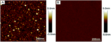 |
| | Fig. 2 Atomic force microscopy (AFM) image of (A) as deposited NiDE (300 nm) on SiO2/Si-substrate and (B) NiTS. | |
XPS characterization of NiTS and NiTS–SAM
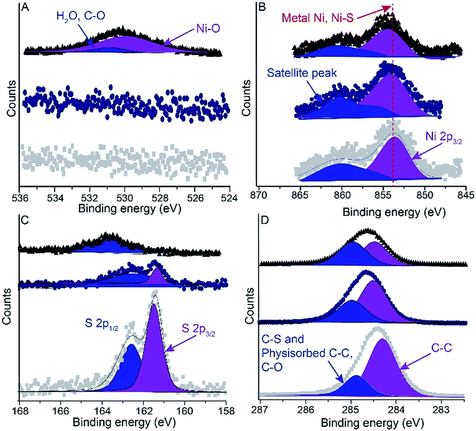
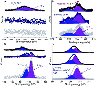
We measured XPS spectra of F 1s to determine whether the NiTS surface contains any residues of the FOTS passivation layer. It is well-known that the C–F bond is prone to radiation damage,48,49 therefore we recorded the high resolution F 1s spectra before the survey scans and the other XPS measurements. Fig. S1† shows the F 1s spectrum and that no F 1s signal could detected which confirms that the NiTS surface is clean and does not contain residues (within the detection limit of our XPS) of the FOTS anti-sticking layer. We further analyzed the NiTS and NiTS–SAM surfaces by XPS to verify the chemical composition of the system with the specific aim to establish whether nickel oxide (NiO) formation was successfully prevented. Fig. 3 shows the oxygen (O 1s), nickel (Ni 2p), sulfur (S 2p), and carbon (C 1s), spectra of the NiTS and NiTS–SAM surfaces and the corresponding binding energies are summarized in Table 1. No clear signals were observed in the O 1s spectra (Fig. 3A) obtained from the NiTS–SAM substrates which confirm that no oxides were present. In contrast, the bare NiTS substrates clearly show an O 1s signal at 529.5 eV corresponding to NiO. The O 1s spectra are in agreement with the Ni 2p3/2 spectra (Fig. 3B) which show that the overlapping metal-oxide (Ni–O) at 854.4 eV is absent for the NiTS–SAM samples and only a Ni–S peak at 853.9 eV can be observed. From these spectra we conclude, that within the detection limits of XPS, that a SAM on oxide free NiTS can be formed. We note, however, that the satellite peak in Fig. 3B is not completely symmetrical which could be caused by a small amount of nickel oxides.
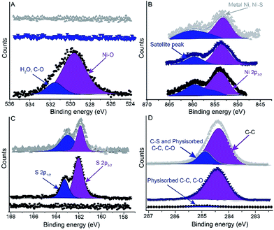 |
| | Fig. 3 XPS spectra of (A) O 1s, (B) Ni 2p, (C) S 2p and (D) C 1s of the (●) bare NiTS, (▼) NiTS-C6 and (▲) NiTS-C14 substrates. | |
Table 1 Measured binding energies of the major core lines of SAMs on NiTS under atmospheric conditions at different time intervals
| Sample |
C 1s (eV) |
O 1s (eV) |
Ni 2pa (eV) |
S 2p (eV) |
F 1s (eV) |
| Binding energy of Ni 2p3/2. |
| NiTS |
285.0 |
529.5, 531.6 |
854.4, 860.0 |
— |
— |
| NiTS-C6 |
284.4 |
— |
853.9, 860.3 |
162.0, 163.2 |
— |
| NiTS-C14 |
284.5, 284.8 |
— |
853.9, 860.3 |
161.4, 162.6 |
— |
| NiTS-C14 (24 h) |
284.5, 284.8 |
— |
854.0, 860.3 |
161.3, 162.4 |
— |
| NiTS-C14 (48 h) |
284.5, 284.9 |
529.8, 530.8 |
854.3, 860.2 |
163.65 |
— |
To confirm the presence of the SAM, we measured the S 2p and C 1s spectra for from the NiTS–SAM substrates. The S 2p spectrum is dominated by a doublet with the main component at 161.4 eV (2p3/2) and the minor component at 162.6 eV (2p1/2). These values are typical for metal-thiolates and these data confirm the presence of the SAM. The C 1s spectra are dominated by a peak at 284.6 eV which is associate with the alkyl chain of the SAM. The weak signal at 285.0 eV for bare NiTS is due to physisorbed carbon contaminants on the NiTS surface. Although the SC6 SAM was dominated by one peak, the SC14 SAM sample had an additional weak signal due to carbon contamination which likely physisorbed during transfer into the XPS chamber. From these data we conclude that both SAMs effectively prevented the formation of nickel-oxides.
Monolayer thickness, tilt angle- and work function of NiTS–SAM
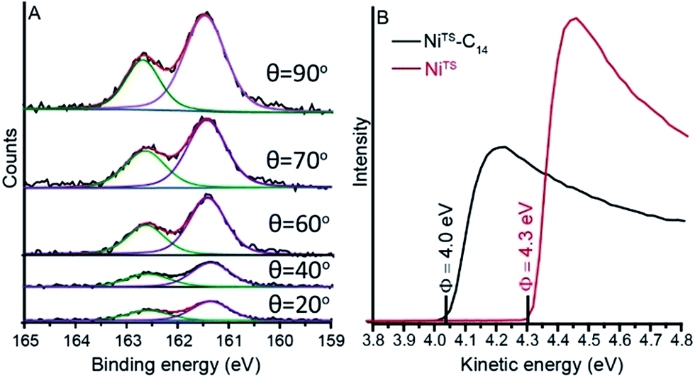
We used angle resolved XPS to determine the SAM thickness, dSAM in nm, on the NiTS following previously reported procedures.39 We recorded S 2p spectra at five different angles ranging from 20° to 90° (Fig. 4A; see ESI†). The value of dSAM for the SC14 SAMs is 1.74 ± 0.2 nm in agreement with previous reports considering a molecular length of 2.17 nm (estimated by CPK model) and a tilt angle with respect to the surface normal of 36 ± 9°.13,34,36
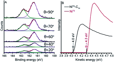 |
| | Fig. 4 (A) XPS of S 2p as a function of the take-off angle of C14 NiTS–SAM and (B) UPS spectra of bare NiTS and a SC14 SAM coated NiTS. | |
We determined the work function Φ of the NiTS–SAM and a freshly prepare native NiTS substrate by ultraviolet photoemission spectroscopy (UPS). We found that the adsorbed monolayer caused a lowering of Φ with respect to the bare NiTS surface of 0.3 eV (Fig. 4B) resulting in a similar value of Φ as of alkanethiolate SAMs on gold and silver likely due to Fermi-level pinning caused by the Ni–S bond.50–52
Stability of Si–FOTS/Ni and NiTS–SAM
In principle, since the Ni is in contact with the template, nickel oxides cannot form. Hence, prior to template-stripping the Ni surfaces can be stored for months without forming NiO. To test this hypothesis, we measured XPS spectra of O 1s (Fig. 5) from a NiTS–SAM surface that was stripped off the Si–FOTS/Ni template after aging of the Si–FOTS/Ni stack for six to eight months in ambient conditions. The O 1s peak was not observed for NiTS–SAM prepared on Si–FOTS/Ni aged up to six months. The NiTS–SAM formed on an 8 month old surface showed an O 1s peak at 529.5 eV which could be due to physisorbed C–O contaminations or NiO. From this observation, in line with observations made by others for AgTS surfaces,39 we conclude that the Ni surfaces can be stored for prolonged periods of time and can be stripped of the template on demand to yield oxide free surfaces in ordinary laboratory conditions.
 |
| | Fig. 5 XPS spectra of O 1s of NiTS–SAM substrate with the NiTS template stripped after storing for (▲) one month, (▼) 6 months and (●) 8 months of the Si–FOTS/Ni stack. | |
The stability of the NiTS–SAM surface upon exposure to atmospheric conditions is important to know and so we followed the rate of oxide formation on the NiTS–SAM over a period of time of 2 days under atmospheric conditions. Fig. 6A shows that after 1 h or 1 day of aging no noticeable amounts of oxides were formed. The ratio of the S 2p peak at 162.6 eV and 161.4 eV is ∼2:1 for NiTS–SAM surface exposed in ambient conditions for 1 hour before transfer into the XPS chamber, the observed ratio is consistent with a metal-bound thiolate species (Fig. 6C). Aging for 2 days, however, caused significant degradation of the sample. The O 1s spectrum showed a peak at 529.8 eV and 530.8 eV corresponding to carbon contamination and Ni–O indicating that Ni surface started to oxidize and the typical signature of a metal-thiolate bond disappeared. We note that the carbon contamination increased with time as is evident from the decrease in the ratio of the two C 1s signals at 284 (C from the SAM) and 285 eV (C from contamination) from 2.4 to 1.1. These results show that the NiTS–SAM surfaces are stable for 1 day.
 |
| | Fig. 6 XPS spectra of O 1s (A), Ni 2p (B), S 2p (C) and C 1s (D) after aging in ambient conditions of (■) NiTS-C14 (1 h), (●) NiTS-C14 (1 day) and (▲) NiTS-C14 (2 days). | |
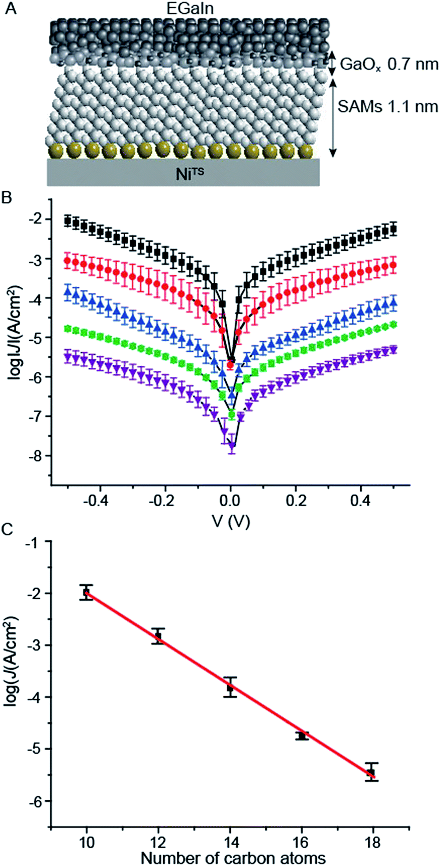
Charge transport studies
To prove that the NiTS surfaces are suitable for applications in molecular electronics, we formed molecular junctions by contacting the NiTS–SAM with cone-shaped EGaIn top-electrodes using well-established procedures.44 Fig. 7A shows the NiTS–SCn//GaOx/EGaIn junction schematically. To determine β of the NiTS–SAM junctions, we prepared SAMs of SCn (with n = 10, 12, 14, 16 and 18) immobilized on NiTS bottom-electrodes (see ESI† and Table 2). We measured the electrical properties of the NiTS–SAM junctions as a function of n (see Experimental section for details) following previously reported procedures.22
 |
| | Fig. 7 (A) Schematic of the NiTS–SAM//GaOx/EGaIn junctions, (B) plot of the log-average value J vs. V of junctions with a SAM of (■) C10, (●) C12, (▲) C14, (![[hexagon filled, point down]](https://www.rsc.org/images/entities/char_e124.gif) ) C16 and (▼) C18 and (C) log|J| vs. carbon chain length at −0.5 V. All error bars represent 95% confident intervals. ) C16 and (▼) C18 and (C) log|J| vs. carbon chain length at −0.5 V. All error bars represent 95% confident intervals. | |
Table 2 Statistical analysis of J(V) measurements of NiTS–SAM//GaOx/EGaIn junctions
| SAMs |
No. of total junctions |
No. of shortsa |
Yieldb |
No. of stable trace |
σlogc |
| A short junction was defined when the value of J exceeded the compliance value of J of our instrument (100 mA) during data collection. The yield is defined as the number of non-shorting junctions divided by the total number of junctions. The σlog is log-standard deviation obtained from Gaussian fitting. |
| C10SH |
17 |
2 |
88 |
375 |
0.44 |
| C12SH |
17 |
0 |
100 |
425 |
0.45 |
| C14SH |
17 |
1 |
94 |
400 |
0.50 |
| C16SH |
14 |
1 |
93 |
325 |
0.34 |
| C18SH |
18 |
2 |
89 |
400 |
0.47 |
| Total |
83 |
6 |
92 |
1925 |
— |
Fig. 7B shows the log-average J(V) curves for each type of junction. We determined the value of β by fitting the data of log|J| vs. n at −0.5 V (Fig. 7C) to the general tunneling equation (eqn (1)). The obtained values of β = 1.01 ± 0.03 nC−1 and log10|J0| = 2.3 ± 0.2 A cm−2 are similar to those values obtained from junctions AuTS or AgTS bottom-electrodes.22,46 These results indicate that the dominant mechanism of charge transport across our junctions is through-bond tunneling,22,47,53,54 where the current flows through the backbone of the alkyl chains of the SAMs. This explains why the values of J of a given molecular length of the SAM are independent of the molecular tilt angles α. In other words, the values of J across junctions with alkanethiolate SAMs on NiTS (α = ∼39° ± 9°) are the same as those with SAMs on AgTS (α = ∼10°) or AuTS (α = ∼30°) substrates.52,53 These results indicate that the overall mechanism of charge transport is dominated by through-bond tunneling, and not through space, which is plausible since through-bond tunneling (β = 0.8 Å−1) is much more efficient than through space tunnelling (β = 2.9 Å−1).20 Our previous studies showed that the value of β decreased from 1.0 nC−1 to 0.4 nC−1 with increasing value of BV from ∼105 nm3 to 107 nm3.39 Thus, here the low BV of the NiTS surfaces (∼2 × 10⁵ nm3) ensured high quality junctions where the SAMs are good tunneling barriers. These junctions have an average yield of non-shorting junctions of 92% and good precision of data with log-standard deviations around 0.3–0.5, similar to the same junctions but with AuTS and AgTS electrodes.
Conclusions
We report a procedure for direct self-assembly of n-alkanethiolate SAMs on oxide-free (within the detection limits of our XPS system) NiTS substrates without using UHV, glove box, or electrochemical reduction methods. The topography of the NiTS surface was determined by AFM and showed that the surfaces were ultra-flat and that the amount of exposed grain boundaries was small. We also showed these surfaces support densely packed SAMs of n-alkanethiolates which, in turn, stabilized the NiTS surface against oxidation in ambient conditions for 1 day. To demonstrate potential applications in molecular electronics, we incorporated the NiTS surface in NiTS–SAM//GaOx/EGaIn junctions and measured the J(V) characteristics. These measurements showed that the SAMs formed high quality tunnelling barriers and the junctions did not suffer from pin holes, with a high yield of non-shorting junctions with good reproducibility. Currently, we are investigating the NiTS surfaces in tunnelling junctions with magnetically active monolayers.
Acknowledgements
Prime Minister's Office, Singapore under its Medium sized centre program is also acknowledged for supporting this research. We also acknowledge the Ministry of Education (MOE) for supporting this research under award No. MOE2015-T2-2-134. The authors thank Dr Xiao-Jiang Yu for help at the Singapore Synchrotron Light Source (SSLS) under NUS core support C-380-003-003-001.
References
- C. Barraud, P. Seneor, R. Mattana, S. Fusil, K. Bouzehouane, C. Deranlot, P. Graziosi, L. Hueso, I. Bergenti, V. Dediu, F. Petroff and A. Fert, Nat. Phys., 2010, 6, 615–620 CrossRef CAS.
- L. Schulz, L. Nuccio, M. Willis, P. Desai, P. Shakya, T. Kreouzis, V. K. Malik, C. Bernhard, F. L. Pratt, N. A. Morley, A. Suter, G. J. Nieuwenhuys, T. Prokscha, E. Morenzoni, W. P. Gillin and A. J. Drew, Nat. Mater., 2011, 10, 252 CrossRef CAS.
- P. Campiglio, R. Breitwieser, V. Repain, S. Guitteny, C. Chacon, A. Bellec, J. Lagoute, Y. Girard, S. Rousset, A. Sassella, M. Imam and S. Narasimhan, New J. Phys., 2015, 17, 063022 CrossRef.
- T. Sergio, G. Marta, D. Sophie, B. Clément, B. Karim, C. Sophie, D. Cyrile, J. Eric, S. Pierre, M. Richard and P. Frédéric, J. Phys.: Condens. Matter, 2016, 28, 094010 CrossRef PubMed.
- P. Tyagi, E. Friebe and C. Baker, J. Nanopart. Res., 2015, 17, 452 CrossRef.
- H. Einati, D. Mishra, N. Friedman, M. Sheves and R. Naaman, Nano Lett., 2015, 15, 1052–1056 CrossRef CAS PubMed.
- I. Carmeli, K. Senthil Kumar, O. Heifler, C. Carmeli and R. Naaman, Angew. Chem., Int. Ed., 2014, 53, 8953–8958 CrossRef CAS PubMed.
- R. Naaman and D. H. Waldeck, Annu. Rev. Phys. Chem., 2015, 66, 263–281 CrossRef CAS PubMed.
- E. A. Weiss, G. K. Kaufman, J. K. Kriebel, Z. Li, R. Schalek and G. M. Whitesides, Langmuir, 2007, 23, 9686–9694 CrossRef CAS PubMed.
- D. Yoo, T. W. Johnson, S. Cherukulappurath, D. J. Norris and S.-H. Oh, ACS Nano, 2015, 9, 10647–10654 CrossRef CAS PubMed.
- L. Jiang, T. Wang and C. A. Nijhuis, Thin Solid Films, 2015, 593, 26–39 CrossRef CAS.
- S. Kumar, T. W. Johnson, C. K. Wood, T. Qu, N. J. Wittenberg, L. M. Otto, J. Shaver, N. J. Long, R. H. Victora, J. B. Edel and S. H. Oh, ACS Appl. Mater. Interfaces, 2016, 8, 9319–9326 CAS.
- A. D. Vogt, T. Han and T. P. Beebe, Langmuir, 1997, 13, 3397–3403 CrossRef CAS.
- P. G. Hoertz, J. R. Niskala, P. Dai, H. T. Black and W. You, J. Am. Chem. Soc., 2008, 130, 9763–9772 CrossRef CAS PubMed.
- S. Devillers, A. Hennart, J. Delhalle and Z. Mekhalif, Langmuir, 2011, 27, 14849–14860 CrossRef CAS PubMed.
- J. R. Niskala and W. You, J. Am. Chem. Soc., 2009, 131, 13202–13203 CrossRef CAS PubMed.
- C. A. Nijhuis, W. F. Reus and G. M. Whitesides, J. Am. Chem. Soc., 2009, 131, 17814–17827 CrossRef CAS PubMed.
- F. C. Simeone, H. J. Yoon, M. M. Thuo, J. R. Barber, B. Smith and G. M. Whitesides, J. Am. Chem. Soc., 2013, 135, 18131–18144 CrossRef CAS PubMed.
- H. B. Akkermann and B. D. Boer, J. Phys.: Condens. Matter, 2008, 20, 013001 CrossRef.
- R. L. McCreery, Chem. Mater., 2004, 16, 4477–4496 CrossRef CAS.
- K. S. Kumar, R. R. Pasula, S. Lim and C. A. Nijhuis, Adv. Mater., 2016, 28, 1824–1830 CrossRef CAS PubMed.
- L. Jiang, C. S. S. Sangeeth, A. Wan, A. Vilan and C. A. Nijhuis, J. Phys. Chem. C, 2015, 119, 960–969 CAS.
- W. F. Reus, C. A. Nijhuis, J. R. Barber, M. M. Thuo, S. Tricard and G. M. Whitesides, J. Phys. Chem. C, 2012, 116, 6714–6733 CAS.
- C. Vericat, M. E. Vela, G. Corthey, E. Pensa, E. Cortés, M. H. Fonticelli, F. Ibañez, G. E. Benitez, P. Carro and R. C. Salvarezza, RSC Adv., 2014, 4, 27730 RSC.
- S. Pookpanratana, L. K. Lydecker, C. A. Richter and C. A. Hacker, J. Phys. Chem. C, 2015, 119, 6687–6695 CAS.
- M. Mattera, R. Torres-Cavanillas, J. P. Prieto-Ruiz, H. Prima-Garcia, S. Tatay, A. Forment-Aliaga and E. Coronado, Langmuir, 2015, 31, 5311–5318 CrossRef CAS PubMed.
- S. Tatay, C. Barraud, M. Galbiati, P. Seneor, R. Mattana, K. Bouzehouane, C. Deranlot, E. Jacquet, A. Forment-Aliaga, P. Jegou, A. Fert and F. Petroff, ACS Nano, 2012, 6, 8753–8757 CrossRef CAS PubMed.
- M. Galbiati, S. Tatay, S. Delprat, C. Barraud, V. Cros, E. Jacquet, F. Coloma, F. Choueikani, E. Otero, P. Ohresser, N. Haag, M. Cinchetti, M. Aeschlimann, P. Seneor, R. Mattana and F. Petroff, Appl. Surf. Sci., 2015, 353, 24–28 CrossRef CAS.
- R. Han, F. Blobner, J. Bauer, D. A. Duncan, J. V. Barth, P. Feulner and F. Allegretti, Chem. Commun., 2016, 52, 9805–9808 RSC.
- O. Ozatay, P. G. Gowtham, K. W. Tan, J. C. Read, K. A. Mkhoyan, M. G. Thomas, G. D. Fuchs, P. M. Braganca, E. M. Ryan, K. V. Thadani, J. Silcox, D. C. Ralph and R. A. Buhrman, Nat. Mater., 2008, 7, 567–573 CrossRef CAS PubMed.
- L. De Los Santos Valladares, A. Ionescu, S. Holmes, C. H. W. Barnes, A. Bustamante Domínguez, O. Avalos Quispe, J. C. González, S. Milana, M. Barbone, A. C. Ferrari, H. Ramos and Y. Majima, J. Vac. Sci. Technol., B, 2014, 32, 051808 Search PubMed.
- T. Y. Chung and S. Y. Hsu, J. Phys.: Conf. Ser., 2009, 150, 042063 CrossRef.
- S. R. Catarelli, S. J. Higgins, W. Schwarzacher, B. W. Mao, J. W. Yan and R. J. Nichols, Langmuir, 2014, 30, 14329–14336 CrossRef CAS PubMed.
- S. Bengió, M. Fonticelli, G. Benítez, A. H. Creus, P. Carro, H. Ascolani, G. Zampieri, B. Blum and R. C. Salvarezza, J. Phys. Chem. B, 2005, 109, 23450–23460 CrossRef PubMed.
- C. Fontanesi, F. Tassinari, F. Parenti, H. Cohen, P. C. Mondal, V. Kiran, A. Giglia, L. Pasquali and R. Naaman, Langmuir, 2015, 31, 3546–3552 CrossRef CAS PubMed.
- F. Blobner, P. N. Abufager, R. Han, J. Bauer, D. A. Duncan, R. J. Maurer, K. Reuter, P. Feulner and F. Allegretti, J. Phys. Chem. C, 2015, 119, 15455–15468 CAS.
- S. Mukhopadhyay and I. Das, Phys. Rev. Lett., 2006, 96, 026601 CrossRef PubMed.
- X. Chen and R. H. Victora, Appl. Phys. Lett., 2007, 91, 212104 CrossRef.
- L. Yuan, L. Jiang, B. Zhang and C. A. Nijhuis, Angew. Chem., Int. Ed., 2014, 53, 3377–3381 CrossRef CAS PubMed.
- C. W. Miller, Z.-P. Li, J. Åkerman and I. K. Schuller, Appl. Phys. Lett., 2007, 90, 043513 CrossRef.
- Z. S. Zhang, J. Appl. Phys., 2004, 95, 557 CrossRef CAS.
- R. H. Victora and X. Chen, IEEE Trans. Magn., 2010, 46, 702–708 CrossRef CAS.
- Z. Mekhalif, F. Laffineur, N. Couturier and J. Delhalle, Langmuir, 2003, 19, 637–645 CrossRef CAS.
- L. Yuan, N. Nerngchamnong, L. Cao, H. Hamoudi, E. del Barco, M. Roemer, R. Sriramula, D. Thompson and C. A. Nijhuis, Nat. Commun., 2015, 6, 6324–6335 CrossRef CAS PubMed.
- C. H. Lee, J. H. Kim, C. Zou, I. S. Cho, J. M. Weisse, W. Nemeth, Q. Wang, A. C. van Duin, T. S. Kim and X. Zheng, Sci. Rep., 2013, 3, 2917 Search PubMed.
- R. C. Chiechi, E. A. Weiss, M. D. Dickey and G. M. Whitesides, Angew. Chem., Int. Ed., 2008, 47, 142–144 CrossRef CAS PubMed.
- L. Yuan, L. Jiang, D. Thompson and C. A. Nijhuis, J. Am. Chem. Soc., 2014, 136, 6554–6557 CrossRef CAS PubMed.
- S. Frey, K. Heister, M. Zharnikov and M. Grunze, Phys. Chem. Chem. Phys., 2000, 2, 1979–1987 RSC.
- O. Zenasni, A. C. Jamison and T. R. Lee, Soft Mater, 2013, 9, 6356–6370 RSC.
- A. S. Erickson, A. Zohar and D. Cahen, Adv. Energy Mater., 2014, 4, 1301724 CrossRef.
- B. Kim, S. H. Choi, X. Y. Zhu and C. D. Frisbie, J. Am. Chem. Soc., 2011, 133, 19864–19877 CrossRef CAS PubMed.
- Y. Qi, O. Yaffe, E. Tirosh, A. Vilan, D. Cahen and A. Kahn, Chem. Phys. Lett., 2011, 511, 344–347 CrossRef CAS.
- H. Song, H. Lee and T. Lee, J. Am. Chem. Soc., 2007, 129, 3806–3807 CrossRef CAS PubMed.
- K. Slowinski, R. V. Chamberlain, C. J. Miller and M. Majda, J. Am. Chem. Soc., 1997, 119, 11910–11919 CrossRef CAS.
Footnote |
| † Electronic supplementary information (ESI) available: Experimental details. See DOI: 10.1039/c6ra27280k |
|
| This journal is © The Royal Society of Chemistry 2017 |
Click here to see how this site uses Cookies. View our privacy policy here. 
 Open Access Article
 This Open Access Article is licensed under a
  *ab
*ab