
 Open Access Article
 This Open Access Article is licensed under a
 Creative Commons Attribution 3.0 Unported Licence
The path of mass transfer during Au thin film-assisted chemical etching by designed surface barriers
Bing Jiang†
a,
Han Dai†a,
Qiang Zhaoa,
Jun Lina,
Lihua Chua,
Yingfeng Lia,
Pengfei Fua,
Gaoxiang Wua,
Jun Jia and
Meicheng Li *ab
*ab
aState Key Laboratory of Alternate Electrical Power System with Renewable Energy Sources, North China Electric Power University, Beijing 102206, China. E-mail: mcli@ncepu.edu.cn; Fax: +86-10-61772951
bSuzhou Institute, North China Electric Power University, Suzhou 215123, China
First published on 14th February 2017
Abstract
The mass transfer in metal-assisted chemical etching between the interfaces has been revealed directly by an epoxy protection method. The results show that the dissolution of Si occurs in the Au film surface instead of the Au–Si interface. A mass transfer path inside the Au film is proposed, in which the Si atoms dissolve in the Au film, and then diffuse across the Au lattice, and are oxidized and etched away at the Au film/solution interface. This model is proved by the oxidation products of Si atoms (SiO2 and SiF62−) on the surface of the Au thin film. In addition, the abnormal emission of H2 at the Au–Si interface indicates the probability of the diffusion of H atoms inside the Au film during the etching. This work provides a further insight into the mechanism of metal-assisted chemical etching.
1. Introduction
Nanostructures of silicon (Si) are the most important materials for the current functional devices, such as nanoelectronics,1 opto-electronics,2 energy conversion3–7 and storage devices,8 as well as bio- and chemical sensors.9,10 Controllable fabrication of Si nanostructures is a prerequisite for their device applications. In recent years, metal-assisted chemical etching (MacEtch), which is a facile and cost-effective method for fabricating Si nanostructures with size features and controlled orientation, has attracted considerable attention.A lot of Si nanostructures have been prepared by MacEtch, such as Si nanowires, porous Si structures, and combined structures with Si micropillars and nanowires.11–15 Despite the overall etching process in which the effect of noble metal on the anode and cathode reaction are explained, the complex or even conflicted phenomena in etching process still exist. For understanding complex etching phenomena, two main mass transfer models during etching process were proposed.16 The assumptions in the models describe the different evolution of oxidization and dissolution of Si atom in etching process. In Model I, it has been speculated that Si atoms are oxidized and dissolved at the interface between the noble metal and the Si substrate and that the reagent and byproduct diffuses along this interface. However, even though difficulties in observing in situ etching process, there are experiment results support this assumption.17 Model II is another possibility concerning mass transfer, in which the Si atoms that contacting with a noble metal are dissolved in the noble metal and then diffuse through the noble metal to the solution where the silicon atoms are oxidized and etched away at the noble metal/solution interface. As yet, there is no direct evidence in the literature proving unambiguously which of the two diffusion processes dominates the metal-assisted chemical etching. In this paper, a series of experiments are designed to reveal the process of mass transfer during the metal-assisted chemical etching, which can be used to understanding the etching process.
2. Experimental details
The p-Si (100) single crystal wafers with resistivity of ρ ∼ 7–13 Ω cm were purchased from Emei Semiconductor Factory, China. Single-polished wafers were cut into 3.0 cm × 1.0 cm pieces and used for the experiments. Using the Al foil template, the Au films with 0.5 cm × 0.5 cm areas and 100 nm thickness were deposited on the Si substrate by the physical vapor deposition. Then, the specimens were annealed at 110 °C for 1 hour. After that, the epoxy drops were dropped on the surface of Au thin film as the barrier layers, as shown in Fig. 1a and b. Fig. 1c shows an epoxy drop on the Au film surface observed by optical microscope. Finally, the Au film was used as the catalyst to etch Si nanostructures by two different etching processes. One is that putting the whole specimen into the etchant solution consisted of HF, H2O2 and H2O for 30 s. Fig. 1d shows the picture of specimen after etching in the solution. The other one is that directly dropping one or two dips of etchant solution on the Au surface for 30 s. After etching, the Au film in the specimen was cleaned by high concentration acid solution and the epoxy was removed by acetone. The morphology of the Si nanostructures after etching was characterized by optical microscope (OM, Yongxiang corp., Model 10XB-PC), scanning electron microscope (SEM, FEI Quanta 200F) and atomic force microscope (AFM, Agilent 5500). The components of byproducts after etching reaction were characterized by X-ray photoelectron spectroscopy (XPS, VG Scientific Ltd. Model ESCALAB MK II). | ||
| Fig. 1 The schematic image and the pictures of the epoxy drops on the specimen. (a) Schematic image of specimen (b) the photo of the epoxy drops on the square Au films; (c) the micrograph of an epoxy drop on the Au film observed by optical microscope (d) the photo of the specimen after etching in the etchant solution. | ||
3. Results and discussion
Obviously, the main discrepancy between Model I and Model II is the different diffusion path of Si in etching process. Therefore, the methods of hindering the diffusion path of Si can be used to reveal the mass transfer mechanism in MacEtch process. In this work, the epoxy drops were used as the barriers to explore the diffusion path of Si during the etching process.In the first etching process, the specimen was directly put into the solution. After etching inside the solution, there are two different etching areas under Au film with and without epoxy, as shown in Fig. 1d. Fig. 2a and b show the morphology of the epoxy drop on the Au film and the Si surface after etching in the same position, which is observed by optical microscope. In Fig. 2b, the dark areas are the Si substrates have been etched, demonstrated by the anti-reflectance property of porous Si. Apparently, the bright area that has similar shape with the epoxy drop has been less affected by the etching solution. Through the SEM observation, Si substrate with the epoxy protection still contains the similar morphology to the original Si surface, as shown in Fig. 3b and c. However, the typical porous Si is observed on the surface under Au film without epoxy, as shown in Fig. 3b and d. The results show that Au film acts as a catalyst to induce the etching of Si substrate. If Model I works, Si could dissolve at the Au/Si interface due to the diffusion of reagent and byproduct, even though the epoxy covers the Au film.16 In this assumption, the Si substrate under Au film catalyst should be also etched, even though the epoxy covers the Au film. However, the results show that the epoxy drops on the Au film actually block the etching process, so that the corresponding areas on Si substrate won't be etched, even though the Si substrate contacts directly to Au film. The results give a proof of Model II for mass transfer, in which the back bonds of the Si atoms at the Au/Si interface and Au are broken; the free Si atoms are dissolved into the noble metal, diffuse through Au film, and are thermally oxidized and etched away at the Au film/solution interface. In this experiment, the epoxy drops on the Au film are as the barriers for diffusion and dissolution of Si atoms, resulting in Si substrate of this area cannot be etched.
 | ||
| Fig. 2 The morphology of the Au film surface and Si surface before and after etching. (a) Optical microscopy image of epoxy drop on Au film before etching; (b) Si substrate after etching. | ||
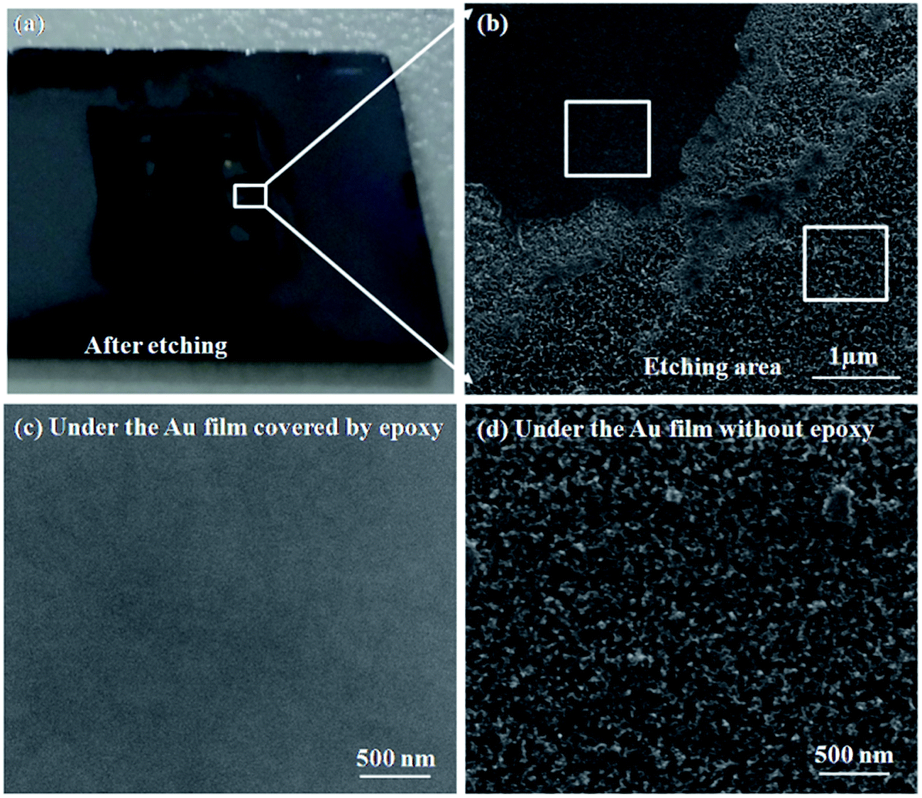 | ||
| Fig. 3 Morphology on different areas with and without epoxy of the Si substrate after etching. (a) The specimen after etching; (b) the etching area on the edge of epoxy; (c) Si substrate under the Au film with epoxy; (d) Si structures under the Au film without epoxy. | ||
In previous studies, Si substrates always are immerged into the etchant solution during most of the etching reactions.18–20 In the solution, the etchant could flow to the Au/Si interface from the out edge of Au film. In order to avoid the flowing of etchant solution, we use another special etching process, in which one or two dips of etchant solution were directly dropped on the top of Au film and no flowing to the edge of Au film. After etching about 30 s, the following process is similar to the specimen etched inside solution. Compared with the reaction inside the solution, the similar results are achieved by etchant dropping, in which the Si substrate with the epoxy protection is not etched. The surface roughness of Si substrate before and after etching is characterized by atomic force microscope (AFM), as shown in Fig. 4. The AFM analysis shows that the roughness of Si nanostructures without epoxy is about 14.8 nm after etching, which is larger than that of original Si and the Si substrate with epoxy protection (roughness is about 1 nm). Obviously, the epoxy covers efficiently hinder the etching reaction of Si substrate underneath it. This result shows that the Si atoms cannot directly transfer into the solution due to the Au barrier between the solution and Si substrate, which excludes the mass transfer path of Model I.
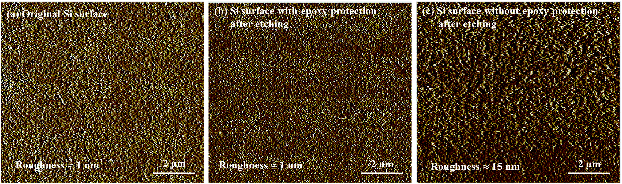 | ||
| Fig. 4 AFM image of (a) original Si substrate; (b) the Si surface under the epoxy protection after etching; (c) the Si surface without the epoxy protection after etching. | ||
The direct contact between Au and Si leads to form Au–Si bonds which could weaken the Si–Si bonds. In fact, the direct penetration of Si atoms through Au thin films has been reported previously.21 Thus, it is possible for Si atoms to diffuse through the Au film, then are oxidized to SiO2 and reacted with HF to produce H2SiF6 on the surface of Au film. To prove the assumption of Model II, the byproducts on the surface of Au film before and after etching are investigated through the XPS analysis. The Au film surface after etching was treated by KOH solution before XPS test, because the main product of H2SiF6 is a volatile chemical, which is hard to characterize after etching. The results show that there is no information of other elements besides Au before etching. While after etching, the SiF62− and SiO2 have been investigated on the top of Au thin film, as shown in Fig. 5a, b, d and e. Therefore, in our experiments Si atoms actually diffuse through the Au film and produce to H2SiF6 on the surface of Au film instead of the Au/Si interface. Moreover, the peak shift of Au 4f has been also found and the reason will be discussed below.
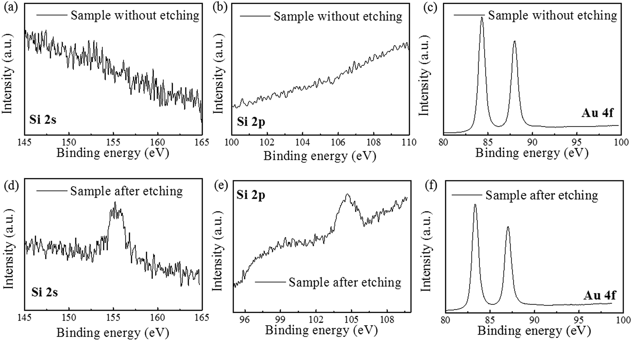 | ||
| Fig. 5 XPS result on the Au film surface (a–c) before etching and (d–f) after etching. (a), (b), (d) and (e) show the change of SiF62− and SiO2; (c) and (f) show the shift of the peak of Au 4f. | ||
During the etching process, it was found that some gases assemble on the Si substrate under the Au film and then release and damage the Au film during the etching, as shown in Fig. 6. The large holes on Au film in the Fig. 6a may be caused by the releasing of the gases during the etching. In the edge of the holes, there are some bulges on Au film, which are caused by the gas which not yet released from the Au/Si interface, as shown in Fig. 6b. This result may be related to the reaction product of H2, which is from the H+ in general cathode reaction proposed in literature.22,23 However, the transfer path of H+ is not yet clear, because during the etching process in solution, the etchant may diffuse from the out edge of Au film to the Au–Si interface. Therefore, the surface cracks on Au thin film are investigated by SEM, AFM and XPS respectively. The results show that there is no obvious crack on Au thin film and roughness of Au thin films is about 1 nm by AFM. In order to avoid missing observation of the molecular scale cracks in a larger range (about mm2), XPS analysis is also used to test the surface of the Au thin film. In the Fig. 5c, the only signal of Au on the surface before etching shows that the Au film has a good molecular scale density. Moreover, the shift of the peak of Au 4f in Fig. 5f attributes to the formation of the Au compound. Therefore, the intensely etching reaction observed in our experiments cannot be supported by the infiltration of HF through the Au thin film. Actually, the H+ in some way diffuses through the Au film and produces the H2 at the Au/Si interface. Similar to the electrochemical penetration of H atoms in Al foil, the penetration of H atoms on the Au film in the acidic solution can be expressed below:24
| Au + H+ + e− = AuH | (1) |
 | (2) |
 | ||
| Fig. 6 Optical image of the assemble of H2 under the Au film and the damage of the Au film caused by the release of H2 (a) optical image in the center area of the H2 bubble; (b) optical image in marginal area. | ||
Moreover, the dynamic of the release of H2 in the interface of Si/Au is complex, which is related to both the vacant left after Si atoms diffusion and surface barrier of reaction products SiO2 on Au surface.
Based on above results, it is found that the mass transfer in metal assisted Si etching process is mainly vertical to the surface in the initial period, which is similar to Model II. Fig. 7 shows the schematic diagram of the mass transfer model. The significant difference from the Model I is the transfer and diffusion of Si and H atoms inside the Au film. It is worth to note that this vertical mass transfer model in only effective in the initial period of the etching process. With increase of the etching time, the morphology of Au thin film is broken by H2 product, which leads to the transverse transfer of the etchant solution between Au/Si interfaces. At the moment, the vertical transfer of Si atoms and the transverse transfer of the etchant solution between Au/Si interfaces occur simultaneously. The massive etchant solution can diffuse into the Au/Si interfaces, which leads to the bad contact of Au–Si. During this etching period, the typical electrochemical reaction indicates that the transverse transfer of the etchant solution between Au/Si interfaces could dominate the etching process.
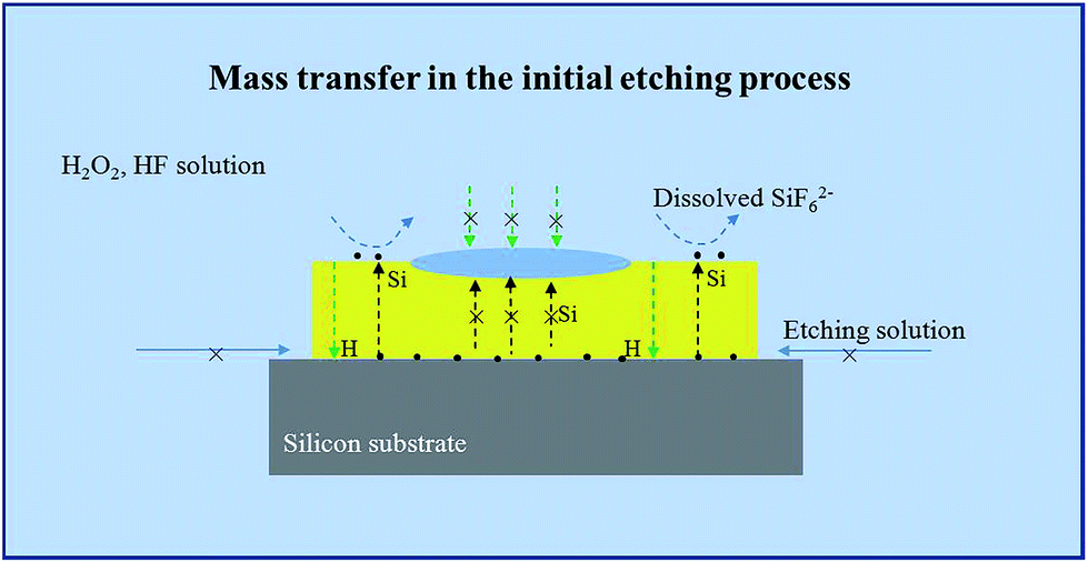 | ||
| Fig. 7 Schematic image of mass transfer during the initial etching process. The reaction occurs at the interface of Au film and solution: Si atoms diffuse through the Au film and produce to H2SiF6 on the surface of Au film; H+ in some way diffuses through the Au film and produces the H2 at the Au/Si interface. | ||
4. Conclusion
In summary, a series of experiment are designed to investigate the mass transfer and etching mechanism during metal-assisted etching process. For the etching process with Au film as the catalyst, the surface protect layer can hinder the diffusion path of Si atoms, which reveals the mass transfer model in MacEtch process. The results show that the intense etching reactions occur in the interface between the Au film and Si surface, which do not contact directly with the etchant solution. That is, the dominate reaction dynamics of Si etching is the diffusion of Si atoms through Au film, which is consistent with the Model II of mass transfer in literature. Meanwhile, we found that H ions transfer and diffuse in the interface between Si/Au and produce H2, which leads to the damage of Au film. The results give the better understanding for mass transfer during the initial etching process. Looking forward, the epoxy protection on catalyst could be used to the more accurate morphology-controlled fabrication of Si nanostructures.Acknowledgements
This work is supported partially by National High-tech R&D Program of China (863 Program, No. 2015AA034601), National Natural Science Foundation of China (Grant no. 91333122, 61204064, 51202067, 51372082, 51402106 and 11504107), PhD. Programs Foundation of Ministry of Education of China (Grant no. 20130036110012), Par-Eu Scholars Program, and the Fundamental Research Funds for the Central Universities (Grant no. 2015ZD07).References
- V. Schmidt, H. Riel, S. Senz, S. Karg, W. Riess and U. Gösele, Realization of a Silicon Nanowire Vertical Surround-Gate Field-Effect Transistor, Small, 2006, 2, 85–88 CrossRef CAS PubMed.
- B. Tian, X. Zheng, T. J. Kempa, Y. Fang, N. Yu, G. Yu, J. Huang and C. M. Lieber, Coaxial silicon nanowires as solar cells and nanoelectronic power sources, Nature, 2007, 449, 885–889 CrossRef CAS PubMed.
- K. Peng, A. Lu, R. Zhang and S.-T. Lee, Motility of Metal Nanoparticles in Silicon and Induced Anisotropic Silicon Etching, Adv. Funct. Mater., 2008, 18, 3026–3035 CrossRef CAS.
- Z. Huang, T. Shimizu, S. Senz, Z. Zhang, X. Zhang, W. Lee, N. Geyer and U. Gösele, Ordered Arrays of Vertically Aligned [110] Silicon Nanowires by Suppressing the Crystallographically Preferred <100> Etching Directions, Nano Lett., 2009, 9, 2519–2525 CrossRef CAS PubMed.
- F. Hui, L. Xudong, S. Shuang, X. Ying and Z. Jing, Fabrication of slantingly-aligned silicon nanowire arrays for solar cell applications, Nanotechnology, 2008, 19, 255703 CrossRef PubMed.
- D. Kumar, S. K. Srivastava, P. K. Singh, M. Husain and V. Kumar, Fabrication of silicon nanowire arrays based solar cell with improved performance, Sol. Energy Mater. Sol. Cells, 2011, 95, 215–218 CrossRef CAS.
- F. Bai, M. Li, D. Song, H. Yu, B. Jiang and Y. Li, One-step synthesis of lightly doped porous silicon nanowires in HF/AgNO3/H2O2 solution at room temperature, J. Solid State Chem., 2012, 196, 596–600 CrossRef CAS.
- K. Q. Peng, J. S. Jie, W. J. Zhang and S. T. Lee, Silicon nanowires for rechargeable lithium-ion battery anodes, Appl. Phys. Lett., 2008, 93 Search PubMed.
- Y. Cui, Q. Wei, H. Park and C. M. Lieber, Nanowire Nanosensors for Highly Sensitive and Selective Detection of Biological and Chemical Species, Science, 2001, 293, 1289–1292 CrossRef CAS PubMed.
- F. Patolsky, G. Zheng and C. M. Lieber, Fabrication of silicon nanowire devices for ultrasensitive, label-free, real-time detection of biological and chemical species, Nat. Protoc., 2006, 1, 1711–1724 CrossRef CAS PubMed.
- F. Bai, M. Li, R. Huang, Y. Li, M. Trevor and K. P. A. Musselman, One-step template-free approach to achieve tapered silicon nanowire arrays with controllable filling ratios for solar cell applications, RSC Adv., 2014, 4, 1794–1798 RSC.
- F. Bai, M. Li, R. Huang, D. Song, B. Jiang and Y. Li, Template-free fabrication of silicon micropillar/nanowire composite structure by one-step etching, Nanoscale Res. Lett., 2012, 7, 1–5 CrossRef PubMed.
- L. Li, Y. Liu, X. Zhao, Z. Lin and C.-P. Wong, Uniform Vertical Trench Etching on Silicon with High Aspect Ratio by Metal-Assisted Chemical Etching Using Nanoporous Catalysts, ACS Appl. Mater. Interfaces, 2013, 6, 575–584 Search PubMed.
- S. Yae, Y. Morii, N. Fukumuro and H. Matsuda, Catalytic activity of noble metals for metal-assisted chemical etching of silicon, Nanoscale Res. Lett., 2012, 7, 352–358 CrossRef PubMed.
- B. Jiang, M. Li, Y. Liang, Y. Bai, D. Song, Y. Li and J. Luo, Etching anisotropy mechanisms lead to morphology-controlled silicon nanoporous structures by metal assisted chemical etching, Nanoscale, 2016, 8, 3085–3092 RSC.
- Z. Huang, N. Geyer, P. Werner, J. de Boor and U. Gosele, Metal-assisted chemical etching of silicon: a review, Adv. Mater., 2011, 23, 285–308 CrossRef CAS PubMed.
- G. Liu, K. L. Young, X. Liao, M. L. Personick and C. A. Mirkin, Anisotropic Nanoparticles as Shape-Directing Catalysts for the Chemical Etching of Silicon, J. Am. Chem. Soc., 2013, 135, 12196–12199 CrossRef CAS PubMed.
- Z. Huang, X. Zhang, M. Reiche, L. Liu, W. Lee, T. Shimizu, S. Senz and U. Gösele, Extended Arrays of Vertically Aligned Sub-10 nm Diameter [100] Si Nanowires by Metal-Assisted Chemical Etching, Nano Lett., 2008, 8, 3046–3051 CrossRef CAS PubMed.
- Z. Zuo, G. Cui, Y. Shi, Y. Liu and G. Ji, Gold-thickness-dependent Schottky barrier height for charge transfer in metal-assisted chemical etching of silicon, Nanoscale Res. Lett., 2013, 8, 1–7 CrossRef PubMed.
- K. Peng, W. Yin, F. Hui, X. Zhong, X. Ying and Z. Jing, Uniform, axial-orientation alignment of one-dimensional single-crystal silicon nanostructure arrays, Angew. Chem., 2005, 44, 2737–2742 CrossRef CAS PubMed.
- A. Cros, J. Derrien and F. Salvan, Catalytic action of gold atoms on the oxidation of Si(111) surfaces, Surf. Sci. Lett., 1981, 110, A356–A357 CrossRef.
- X. Li and P. W. Bohn, Metal-assisted chemical etching in HF/H2O2 produces porous silicon, Appl. Phys. Lett., 2000, 77, 2572–2574 CrossRef CAS.
- Y. Harada, X. Li, P. W. Bohn and R. G. Nuzzo, Catalytic Amplification of the Soft Lithographic Patterning of Si. Nonelectrochemical Orthogonal Fabrication of Photoluminescent Porous Si Pixel Arrays, J. Am. Chem. Soc., 2001, 123, 8709–8717 CrossRef CAS PubMed.
- X. Wang and L. Andrews, Infrared Spectra and DFT Calculations for the Gold Hydrides AuH, (H2)AuH, and the AuH3 Transition State Stabilized in (H2)AuH3, J. Phys. Chem. A, 2002, 106, 3744–3748 CrossRef CAS.
Footnote |
| † These authors contributed equally to this work. |
| This journal is © The Royal Society of Chemistry 2017 |