
 Open Access Article
 This Open Access Article is licensed under a
 Creative Commons Attribution 3.0 Unported Licence
Grain size reduction on nanostructured TiO2 thin films due to annealing
Zaki S. Khalifa
Department of Physics, Beni-Suef University, Beni-Suef 62111, Egypt. E-mail: zaki.khalifa@science.bsu.edu.eg; Fax: +20822334551; Tel: +201004829670
First published on 12th June 2017
Abstract
TiO2 thin films have been deposited at 300 °C on quartz substrates by a metal–organic chemical vapor deposition technique. The obtained films have been annealed at different temperatures up to 1100 °C. X-ray diffraction studies show that the obtained films maintain the anatase phase till 800 °C annealing temperature, and the rutile phase appears at 900 °C. Extra unidentified peaks appear at 1000 °C, and 1100 °C. Raman microscopy has been used to identify the obtained films. The obtained spectra show the normal modes of vibrations of the pure and mixed phases. Scanning electron microscopy graphs show grain size shrinkage concurrent to the appearance of the rutile phase. A slight band gap reduction has been calculated from UV-Vis transmittance spectrophotometery measurements. DC conductivity curves show three regions with different activation energies.
1. Introduction
TIO2 thin films have been involved in many applications such as electrochromism,1 lithium batteries,2 photocatalysis,3 H2 production,4 dye sensitized solar cells,5 and gas sensing.6 The optical and electrical properties of the TiO2 thin films depend on the structure and morphology of the deposited material which is dictated beside the preparation method by the preparation conditions, and/or post deposition treatments. Moreover, specific applications rely on the crystalline structure and morphology of the active material. For example, the anatase phase shows better electrochemical properties than rutile,7 while the mixed phase shows better photon to electron conversion properties than both single phases.8 Raising the deposition temperature causes structural and morphological changes in the TiO2 nanoparticles. They include amorphous to crystalline, and phase to phase transformations.9TiO2 has three famous polymorphs, anatase, brookite, and rutile. They consist of octahedra shared by edges and corners. Octahedron has 12 edges. In anatase 4 of these edges are shared with neighboring octahedra, but in rutile only 2 are. At the same time, the anatase octahedron is corner shared with 8 octahedra, while rutile is shared by 4. Anatase has 4 polyhedra per unit cell, and rutile has 2. All these structure differences have their impact on the electronic structure which can be investigated by optical and electrical measurements. Phase transformation among the above mentioned TiO2 three polymorphs has been studied before.9,10 In fact, if we need a better understanding of phase transformations we have to think about Gibbe's free energy function. In other words, thermodynamics will enable us to collect the affecting parameters in phase transformation in one equation. Change in Gibbe's free energy for bulk is the difference between the standard free energy of formation of the individual phases.11,12 In the nanoscale additional terms should be added so:13
| ΔGA–R = (ΔGv,R(T) − ΔGv,A(T)) + (γRAR − γAAA) + (ΔPRVR − ΔPAVA) | (1) |
The driving force for this transformation usually is the increase of annealing temperature12,21 but combination of pressure and temperature also control this transformation for deposition processes.9,10,24 Moreover, super-saturation can be achieved by controlling the precursor solution environment. In other words, chemical potential, and the number of moles, or equivalently the chemical activities of the reactants, and products can play a significant role in the phase, and shape of the deposited TiO2 films. Roy et al.25 have studied not only the deposition conditions but also the properties of TiO2 thin films produced by solution bath deposition method. This can be translated as another term in eqn (1).
This study aims to explore the effect of annealing temperature on the structure, morphology, optical, and electrical properties of TiO2 thin films prepared by MOCVD.
2. Material and methods
2.1. Preparation of the films
Thin films of TiO2 have been deposited on quartz substrates by a hot wall chemical vapor deposition technique at temperature 300 °C. 25 × 12 × 1 mm quartz substrates have been used. Before loading, the substrates have been washed by detergent, distilled water, acetone, and isopropyl alcohol. The reactor consists of a stainless steel tube attached from one side to a pressure gauge, and a mechanical pump, and from the other side to oxygen, and precursor inlets. It has been put in a horizontal furnace. The precursor is titanium tetra isopropoxide, TTIP 97 +% pure, Alfa Aesar, USA. A 0 Torr pressure has been maintained in the reactor during heating. After that O2 has been introduced to the reactor, with a rate ranges from 30–33 scccm, to clean the substrates, and increase the reactivity of the precursor. TTIP has been heated at 80 °C, and then carried to the reactor by Ar gas tell the pressure reached 15 Torr (2 kPa). Post deposition annealing has been carried out for 2 hours in air using a muffle furnace at temperatures ranging from 400 °C to 1100 °C.2.2. Characterization of the films
Structural characterizations of the TiO2 thin films have been carried out by X-ray diffraction (XRD). θ − 2θ scans have been recorded using Cu Kα radiation in a Rigaku D-Max B diffractometer equipped with a graphite crystal monochromator. 2θ ranges from 20° to 70°. Raman spectroscopy has been recorded using Senterra Raman microscope, Bruker. A laser source of 532 nm wavelength has been used. Its power has been adjusted to be 10 mW. Thickness and morphology of the films have been measured by field emission scanning electron microscope, (FEI, Quanta 250 FEG). Optical transmission measurements have been carried out using a JASCO UV-350 spectrophotometer in the range from 300 to 1100 nm. Films have been annealed in air using a controlled temperature furnace. To measure the DC conductivity, two gold electrodes have been sputtered at the edges of the film to obtain ohmic contacts. Resistance has been measured by Keithly 612 electrometer as a function of temperature, and the corresponding DC conductivity has been calculated.3. Results and discussions
3.1. Structure and morphology
XRD diffractograms for the as deposited sample, and those annealed up to 1100 °C are shown in Fig. 1. Using the powder diffraction files to identify the phase of the deposited and annealed films, it has been found that anatase is the only existing phase till 800 °C, and rutile appears at 900 °C.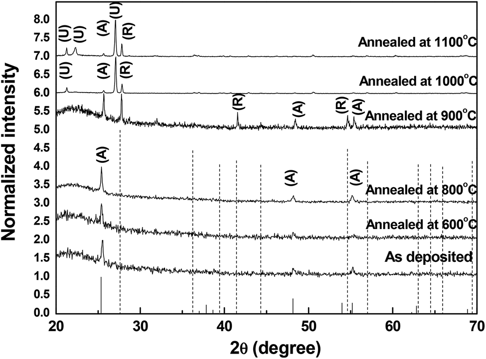 | ||
| Fig. 1 X-ray diffraction patterns of the as-deposited TiO2 film and films annealed up to 1100 °C. | ||
The phase is mixed until 1100 °C. Something unexpected appears in these samples, which is the appearance of extra peaks in the samples annealed at 1000 °C and 1100 °C. To make sure, XRD investigation of quartz annealed at 1100 °C has been run. The obtained pattern does not show any peaks. The annealing process and the XRD measurements have been repeated without change in the results. In Fig. 1, the strongest peak (101) lies at 2θ equals 25.55°. Referring to powder diffraction file with reference code number 89-4921, one can find that the peak position of the main anatase peak is equal to that of the as deposited sample. This peak exists even if the sample annealed up to 1100 °C. At annealing temperature 900 °C the main rutile peak appears at 2θ equals 27.8°, which agrees with the standard peak found in powder diffraction file number 88-1172.
Two extra peaks appear in the sample annealed at 1000 °C. One of them is shown at 21.3° and the other at 27°. A third unidentified peak appears at 22.3° in the film annealed at 1100 °C. The appearance of unidentified peak close to 22° has been reported before for a sample deposited by sputtering.26 But the appearance of another peak close to 27° has not been reported before. The crystallite size has been found to be 44 nm according to Debye–Sherrer equation.1 This crystallite size is large compared to that of other nanoparticles prepared by the same technique.13 Complete transformation to rutile depends on the anatase particle size, since small particles transform faster.13 This may be the reason why rutile is not pure in this range of annealing. Such a delay in the rutile phase complete transformation has been attributed to the competition between two effects.27 With the increase of annealing temperature, rutile phase nucleates, and grows also, the boundaries between crystallites at which anatase transforms to rutile decreases in volume. This reduction limits the nucleation, and growth of the rutile phase as seen in the XRD charts.
Since the anatase peaks diminish at high annealing temperatures, then the extra peaks may identify another form of rutile. We have to consider the relative intensity of the peak noticed at 2θ = 27°. In other words, a new diffraction pattern of rutile is obtained in this study.
To assert the above conclusion, Raman spectra of the as deposited, and some of the annealed samples have been run, and presented in Fig. 2. Table 1 gives the peak positions of the Raman shifts.
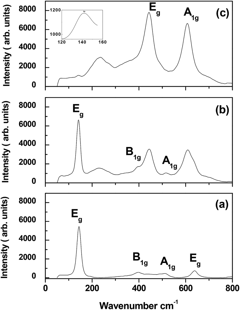 | ||
| Fig. 2 Raman spectra for samples (a) as deposited, (b) annealed at 900 °C, and (c) annealed at 1100 °C. | ||
| As-deposited | 900 °C | 1100 °C | Assignation |
|---|---|---|---|
| 143.5 cm−1 | 141.5 cm−1 | 142 cm−1 | Eg (anatase) low frequency |
| — | 229.5 cm−1 | 235.5 cm−1 | — |
| 397.5 cm−1 | — | — | B1g (anatase) |
| 443.5 cm−1 | 443.5 cm−1 | Eg (rutile) | |
| 511.5 cm−1 | — | A1g (anatase) | |
| — | 609.5 cm−1 | 607 cm−1 | A1g (rutile) |
| 639 cm−1 | — | — | Eg (anatase) high frequency |
Raman studies confirm XRD results. As shown in Fig. 2, the as deposited sample is a pure anatase while the annealed samples are mixed. The low frequency Eg peak appears in all the investigated samples. Also, the B1g, A1g, and the higher frequency Eg modes of vibration characterizing the anatase phase appear in the as deposited sample.14,27,28 Annealing at 900 °C induces peaks mixing. A band is noticed at 229.5 cm−1, and it shows a blue shift with the increase of annealing temperature. This band is a higher order mode of vibration, and has been called a two phonon band.29,30
The film annealed at 1100 °C demonstrates a low existence of the Eg anatase mode of vibration compared to the Eg and A1g modes of the rutile phase.
From the spectrum depicted in Fig. 3, it can be noticed that there is no any other peak except a small hump at 826 cm−1 which can be attributed to the B2g mode of vibration of rutile.31 This spectrum confirms the above conclusion about the new diffraction pattern of rutile obtained in this study.
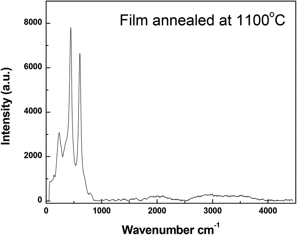 | ||
| Fig. 3 The complete spectrum of the film annealed at 1100 °C. | ||
The thickness of the films has been determined by measuring the cross section of the annealed films. For example, the thicknesses of the 600 °C, and 900 °C annealed films have been found to be 250 ± 5 nm and 260 ± 10 nm, respectively.
The morphology of the films has been monitored by FESEM studies as shown in Fig. 4. The as deposited film consists of clusters of small grains. Due to annealing the small grains coarsen, and fragment, and as a result the morphology has been changed to that shown in Fig. 4b. Such fragmentation has been reported before but for direct deposition with increasing the deposition temperature under the same pressure.10 Further heating at 900 °C shows something unusual for direct annealing. At this stage of phase transformation, the grain size decreases, it seems smaller compared to that of annealed at 600 °C. Not only the size but also the shape of the grains changes due to heating. The grain size increases again when the sample annealed up to 1100 °C.
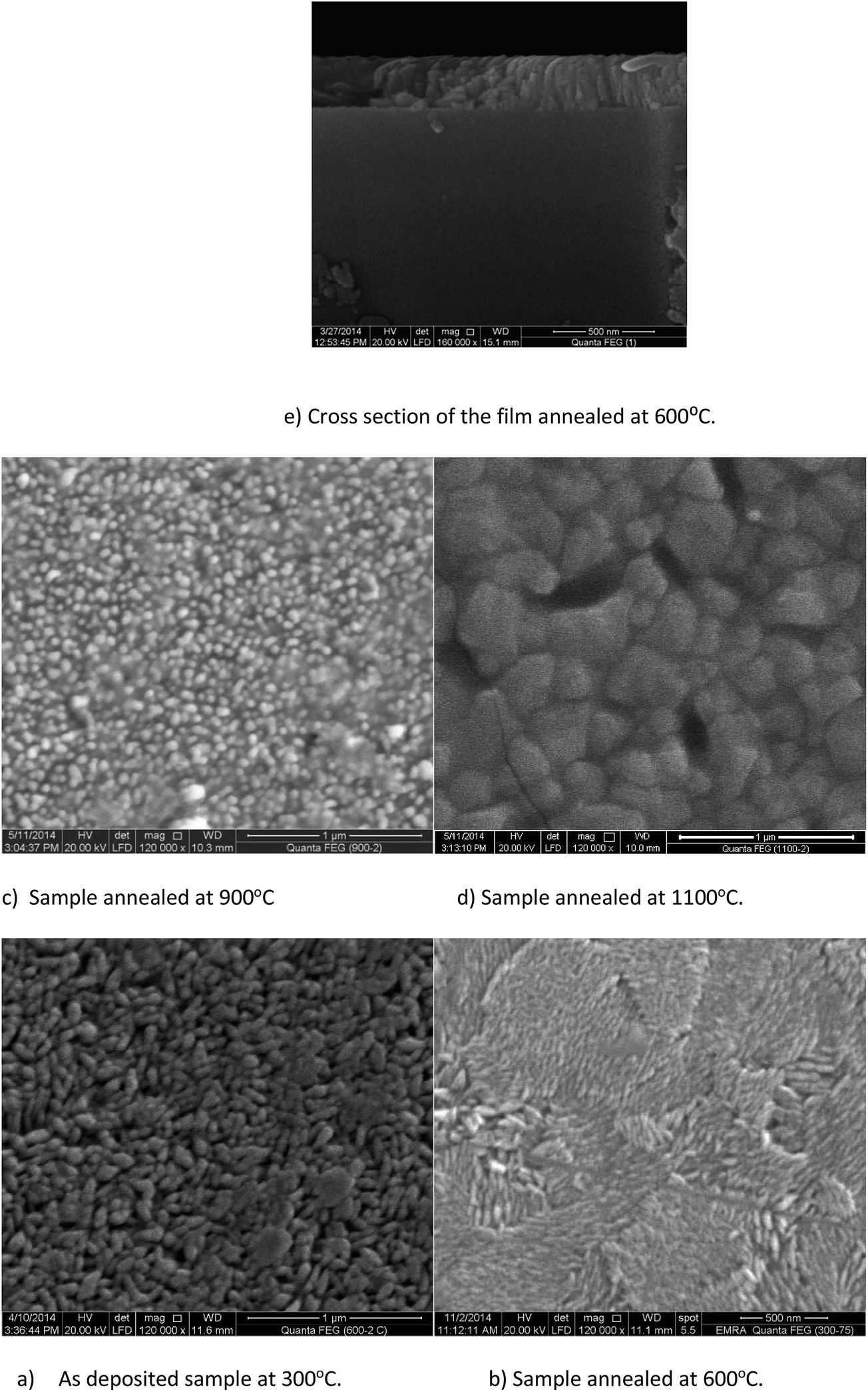 | ||
| Fig. 4 FESEM micrographs of as deposited film, films annealed at temperatures 600 °C, 900 °C, 1100 °C, and the cross section of the film annealed at 600 °C. (a) As deposited sample at 300 °C. (b) Sample annealed at 600 °C. (c) Sample annealed at 900 °C. (d) Sample annealed at 1100 °C. (e) Cross section of the film annealed at 600 °C. | ||
The reported trend of the change in grain size with increasing the annealing temperature is the increase of particle size. This behavior has been elucidated by different tools in many reports. Table 2 shows the temperature ranges in which pure anatase transforms to rutile by sol–gel, spray pyrolysis and sputtering for some studies.
| Deposition technique | Start of transformation | Complete phase transformation temperature | Used technique | Reference |
|---|---|---|---|---|
| MOCVD | 700 °C | — | XRD, SEM | 13 |
| Normal sol–gel | 650 °C, 450 °C sample, big crystallite size | 850 °C, bad defined crystallite sizes | XRD, SEM | 32 |
| Ultrasound assisted sol–gel | 650 °C, for 450 °C sample, small crystallite size, no agglomerations | 750 °C, 850 °C sample lesser, agglomerations and well defined crystallite sizes | XRD, SEM | 32 |
| Sol–gel | 800 °C | 900 °C | XRD, SEM | 33 |
| Spray pyrolysis | 800 °C | 1000 °C | XRD, AFM, SEM 50 nm | 14 |
| Sputtering | 700 °C | 900 °C | XRD, AFM | 34 |
| Sputtering | 650 °C | 750 °C | XRD (23.3 nm), SEM | 35 |
Particle or grain size reduction before the crossover temperature, i.e. for pure anatase, has been reported for films and nanoparticles deposited by MOCVD at higher temperatures.9 This decrease of particle size with the increase of deposition temperature under the same total pressure has been attributed to the increase of nucleation density which suppresses the calcination effects for powder nanoparticles. For thin films another explanation has been reported.10,23 In this study, calcination effects only control the growth of anatase, and the nucleation, and growth of rutile phases. Annealing at higher temperatures did not cause such particle size reduction for nanoparticle samples deposited by the same technique.13 It is clear from the SEM images that calcination effects act traditionally until the appearance of the rutile phase. In other words, coarsening mechanism prevails. During phase transformation grain size reduction takes place. This event has not been reported for annealed films before. For example, Tu and Goto36 reported an increase in the grain size with the increase in annealing temperature without any reduction at the crossover temperature. Won et al.37 deposited TiO2 thin films at the same temperature by the same technique, and precursor with slight deposition condition differences. They did not notice the reported reduction in grain size due to annealing. This may be because the percent of the rutile phase in their mixed phase sample was small as seen in their XRD pattern. If we calculate the weight percent of the rutile at this temperature using the formula:21
| wR = IR/Io = IR/(0.994IA + IR) | (2) |
3.2. Optical properties
UV-Vis spectrophotometric measurements have been carried out for the as deposited sample and those annealed at 600 °C, and 900 °C and presented in Fig. 5.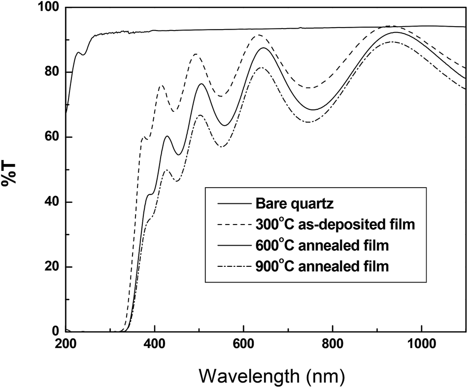 | ||
| Fig. 5 Transmittance spectra as a function of wavelength for bare quartz substrate, as-deposited film and films annealed at 600 °C, and 900 °C. | ||
Absorption coefficient α can be calculated from the relation:
| T = (1 − R)2exp(−αd)/1 − R2exp(−αd) | (3) |
| α = (1/d)ln(1/T) | (4) |
The energy gap for indirect band gap transition can be calculated from:42
| √αhν = (Eg − hν + Eph) + (Eg − hν − Eph) | (5) |
The obtained optical energy gap values are 3.28 eV, 3.2 eV and 3.14 eV for deposition temperature 300 °C and the annealing temperatures 600 °C, and 900 °C, respectively. It is clearly seen that the band gap decreases with the increase of annealing temperature. This behavior is the expected according to that published in literature (Fig. 6).14,37
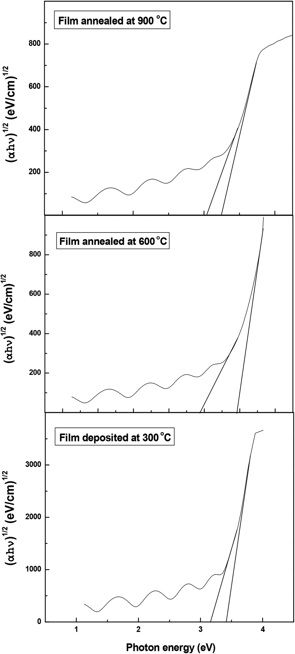 | ||
| Fig. 6 √αhν versus photon energy for as deposited sample and those annealed at 600 °C, and 900 °C. | ||
3.3. Electrical properties
DC conductivity measurements have been run for samples annealed at 600 °C, and 900 °C. The natural logarithm as a function of the reciprocal of absolute temperature is depicted in Fig. 7.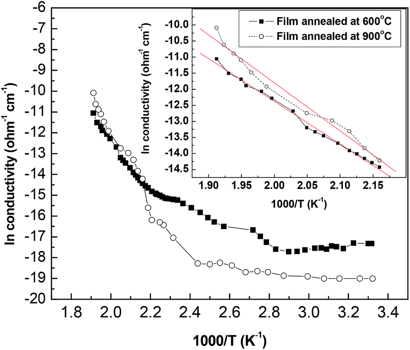 | ||
Fig. 7 ln![[thin space (1/6-em)]](https://www.rsc.org/images/entities/char_2009.gif) σ as a function of 1000/T for samples annealed at 600 °C, and 900 °C. σ as a function of 1000/T for samples annealed at 600 °C, and 900 °C. | ||
It shows that the obtained curve can be divided into three regions. The results do not show smooth curve because of switching between the electrometer ranges. The first part is nearly temperature independent in the range from room temperature to about 130 °C (273–403 K). Temperature independent attitude has been found in the range from 13–230 K for anatase by Mardare and Rusu.43 They attributed the conduction behavior to nonstoichiometry. Anatase sample reduced at 450 °C under vacuum show an insulator to metal transition in the temperature range from 80–280 K.28 Also, highly reduced rutile showed activation energy equals 0.06 eV in the same temperature range.28 At higher temperature in the range from room temperature to 345 K Akl et al. obtained an activation energy equals 0.03 eV.44
An intermediate increase in conductivity takes place in the temperature range from 130 °C to 190 °C (403–463 K). Akl et al. noticed a similar trend with activation energy equals 0.17 eV.44 Deviation from linearity in the curve relating the logarithm of resistivity, and the reciprocal of absolute temperature in the range from 409–463 K has been found by Deshmukh et al.41 In the temperature range from 360–500 K Mardere, and Rusu proved linearity with activation energy equals 0.72 eV.43
High activation energy conductivity prevails in the temperature range from 190 °C to 250 °C (463–523 K). In the later temperature range the activation energy has been calculated from the equation:43
|
lnσ = lnσo − Ea/kT
| (6) |
Activation energy depends on the type of the substrate, grain size, and phase.45–47 Also, the activation energy value depends on the temperature range for which it is calculated.44 Oxygen partial pressure plays a critical role in transport properties of metal oxides.28,44
The three regions obtained in this study resemble those obtained by Akl et al. for samples deposited by reactive RF sputtering but with different values of conductivities, and activation energies.44 This can be attributed to the deposition conditions, and post deposition treatment in the two cases. Deposition of the samples on this study involves reaction in the presence of oxygen at 300 °C, and leaving the samples to cool down to room temperature in the presence of oxygen. Moreover, annealing in this study has been carried out in air, while in their study it has been carried out under vacuum at temperatures 400 °C, 450 °C and 500 °C, respectively. Such annealing reduces the deposited material which causes semiconductor to metal transition for anatase annealed at 450 °C.28 Oxygen vacancies create donor energy states below the conduction band. Depending on the concentration of these created levels Fermi level moves toward the conduction band. So, the activation energy will inversely proportional to the concentration of oxygen vacancies.
It can be concluded that annealing in air and its influences on the structural and morphological properties of TiO2 thin films did not make significant changes on the electrical conductivity, and activation energy of the obtained films if experimental errors have been taken into consideration.43,48
4. Conclusion
TiO2 thin films have been deposited by MOCVD at 300 °C, and subsequently annealed tell 1100 °C. Films deposited, and annealed till 800 °C are pure anatase. Rutile phase starts to appear at 900 °C. Extra unidentified peaks have been detected in the films annealed at 1000 °C, and 1100 °C. SEM micrographs revealed a regular calcination effects but anomalous reduction in the grain size synchronizes the detection of the rutile phase. A new diffraction pattern of rutile has been noticed in this study according to the analysis of the XRD, and Raman data. Optical properties show a regular trend while electrical conductivity suggested three different activation energies.Acknowledgements
The author would like to thank the nano-materials and nanotechnology lab team at Beni – Suef University for their help. Also, I would like to thank Prof. Kamal Abdel-Hady and his group in El-Minia University for their help regarding DC conductivity measurements.References
- Z. S. Khalifa, Sol. Energy Mater. Sol. Cells, 2014, 124, 186 CrossRef CAS
.
- C. Natarajan, N. Fukunaga and G. Nogami, Thin Solid Films, 1998, 322, 6 CrossRef CAS
- F. Men, X. Song and Z. Sun, Vacuum, 2009, 83, 1147 CrossRef
- M. Grätzel, Nature, 2000, 414, 344 Search PubMed
- B. O'Regan and M. Grätzel, Nature, 1991, 353, 737 CrossRef
- H. Kim, M. Hong, H. Jang, S. Yoon and H. Park, Thin Solid Films, 2013, 529, 89 CrossRef CAS
- B. Zachau-Christiansen, K. West, T. Jacobsen and S. Atlung, Solid State Ionics, 1988, 28–30, 1176 CrossRef
- J. M. Wu, H. C. Shih and W. T. Wu, Chem. Phys. Lett., 2005, 413, 490 CrossRef CAS
- W. Li, S. Ismat Shah, M. Sung and C.-P. Huang, J. Vac. Sci. Technol., B, 2002, 20, 2303 CAS
- C. J. Taylor, D. C. Gilmer, D. G. Colombo, G. D. Wilk, S. A. Campbell, J. Roberts and W. L. Gladfelter, J. Am. Chem. Soc., 1999, 121, 5220 CrossRef CAS
- T. L. Hill, Thermodynamics of Small Systems, W. A. Benjamin, New York, NY, 1963, vol. I Search PubMed
- T. L. Hill, Thermodynamics of Small Systems, W. A. Benjamin, New York, NY, 1964, vol. II Search PubMed
- W. Li, C. Ni, H. Lin, C. P. Huang and S. Ismat Shah, J. Appl. Phys., 2004, 96, 6663 CrossRef CAS
- A. Nakaruk, D. Ragazzon and C. C. Sorrell, Thin Solid Films, 2010, 518, 3735 CrossRef CAS
- M. Matsui and M. Akaogi, Mol. Simul., 1991, 6, 239 CrossRef
- S. Smith, R. Stevens, S. Liu, G. Li, A. Navrotsky, J. Boerio-Goates and F. Woodfield, Am. Mineral., 2009, 94, 239 CrossRef
- P. M. Oliver, G. W. Watson, T. E. Kelsey and C. S. Parker, J. Mater. Chem., 1997, 7, 563 RSC
- M. Lazzeri, A. Vittadini and A. Selloni, Phys. Rev. B: Condens. Matter Mater. Phys., 2001, 63, 15540 CrossRef
- M. Lazzeri, A. Vittadini and A. Selloni, Phys. Rev. B: Condens. Matter Mater. Phys., 2002, 65, 11990 Search PubMed
- U. Diebold, N. Ruzycki, G. S. Herman and A. Selloni, Catal. Today, 2003, 85, 93 CrossRef CAS
- A. A. Gribb and J. F. Banfield, Am. Mineral., 1997, 82, 717 CAS
- H. Zhang and J. F. Banfield, J. Mater. Chem., 1998, 8, 2073 RSC
- Z. S. Khalifa, H. Lin and S. Ismat Shah, Thin Solid Films, 2010, 518, 5457 CrossRef CAS
- Y. Sun, A. Li, M. Qi, L. Zhang and X. Yao, Mater. Sci. Eng. B, 2001, 86, 185 CrossRef
- B. Roy, G. Zhang and J. Cho, J. Am. Ceram. Soc., 2012, 95, 676 CrossRef CAS
- D. Yoo, I. Kim, S. Kim, C. Hahn, C. Lee and S. Cho, Appl. Surf. Sci., 2007, 253, 3888 CrossRef CAS
- H. Rath, P. Dash, T. Som, P. Satyam, U. Singh, P. Kulriya, D. Kanjilal, D. Avasthi and N. Mishra, J. Appl. Phys., 2009, 105, 074311 CrossRef
- H. Tang, K. Prasad, R. Sanjinbs, P. Schmid and F. Levy, J. Appl. Phys., 1994, 75, 2042 CrossRef CAS
- C. Rosário, M. Grac, M. A. Valente, L. Costa, J. Rodrigues, T. Monteiro, E. Alves and N. Sobolev, Phys. Status Solidi B, 2013, 250, 843 CrossRef
- B. Santara, P. Giri, K. Imakita and M. Fujii, J. Phys. D: Appl. Phys., 2014, 47, 215302 CrossRef
- C. Chen, Y. Chen, A. Korotcov, Y. Huang, D. Tsai and K. Tiong, Nanotechnology, 2008, 19, 075611 CrossRef CAS PubMed
- K. Prasad, D. V. Pinjari, A. B. Pandit and S. T. Mhaske, Ultrason. Sonochem., 2010, 409, 17 Search PubMed
- A. Nakaruk, C. Y. Lin, D. S. Perera and C. C. Sorrell, Sol-Gel Sci. Technol., 2010, 55, 328 CrossRef CAS
- Y. Hou, D. Zhuang, G. Zhang, M. Zhao and M. Wu, Appl. Surf. Sci., 2003, 218, 98 CrossRef
- B. Sarma, A. Pal, H. Bailung and J. Chutia, J. Alloys Compd., 2013, 577, 261 CrossRef CAS
- R. Tu and T. Goto, Mater. Trans., 2008, 49, 2040 CrossRef CAS
- D. Won, C. Wang, H. Jang and D. Choi, Appl. Phys. A, 2001, 73, 595 CrossRef CAS
- H. Zhang and J. Banfield, Am. Mineral., 1999, 84, 528 CrossRef CAS
- G. Herman and Y. Gao, Thin Solid Films, 2001, 397, 157 CrossRef CAS
- M. Ahmad and S. Bhattacharya, Appl. Phys. Lett., 2009, 95, 191906 CrossRef
- H. P. Deshmukh, P. S. Shinde and P. S. Patil, Mater. Sci. Eng., B, 2006, 130, 220 CrossRef CAS
- A. Kumar, P. Singh, N. Kulkami and D. Kaur, Thin Solid Films, 2008, 516, 912 CrossRef CAS
- D. Mardare and G. Rusu, Mater. Sci. Eng. B, 2000, 75, 68 CrossRef
- A. Akl, H. Kamal and K. Abdel-Hady, Appl. Surf. Sci., 2006, 252, 8651 CrossRef CAS
- B. Huber, H. Gnaser and C. Ziegler, Surf. Sci., 2004, 566–568, 419 CrossRef CAS
- B. Huber, A. Brodyanski, M. Scheib, A. Orendorz, C. Zieglera and H. Gnaser, Thin Solid Films, 2005, 472, 114 CrossRef CAS
- I. Oja, A. Mere, M. Krunks, R. Nisumaa, C.-H. Solterbeck and M. Es-Souni, Thin Solid Films, 2006, 515, 674 CrossRef CAS
- M. Sekhar, P. Kondaiah, S. Chandra, G. Rao and S. Uthanna, Appl. Surf. Sci., 2011, 258, 1796 Search PubMed
| This journal is © The Royal Society of Chemistry 2017 |