
 Open Access Article
 This Open Access Article is licensed under a
 Creative Commons Attribution 3.0 Unported Licence
Pseudo-monocrystalline properties of cylindrical nanowires confinedly grown by electrodeposition in nanoporous alumina templates†
Enrique Díaz Barriga-Castro *a,
Javier Garcíabc,
Raquel Mendoza-Reséndezd,
Víctor M. Pridab and
Carlos Luna*d
*a,
Javier Garcíabc,
Raquel Mendoza-Reséndezd,
Víctor M. Pridab and
Carlos Luna*d
aCentro de Investigación en Química Aplicada (CIQA), Blvd. Enrique Reyna Hermosillo No. 140, Saltillo, 25294 Coahuila, Mexico. E-mail: enrique.diazbarriga@ciqa.edu.mx
bUniversidad de Oviedo, Departamento de Física, Calvo Sotelo s/n, Oviedo, 33007 Asturias, Spain
cInstitute for Metallic Materials, IFW Dresden, Helmholtzstrasse 20, 01069 Dresden, Germany
dUniversidad Autónoma de Nuevo León (UANL), Av. Universidad S/N, San Nicolás de los Garza, 66455, Nuevo León, Mexico. E-mail: carlos.lunacd@uanl.edu.mx
First published on 1st March 2017
Abstract
Four different cylindrical nanowire systems (nickel, cobalt, Co23Cu77, and multisegmented Co58Ni42/Co83Ni17 nanowires) with single-crystal-like properties were characterized by transmission electron microscopy and selected-area electron diffraction (SAED) under different tilting angles. Although these nanowires have different chemical compositions, crystalline structures and/or diameters, they exhibit similar behaviors, which are unexpected for ideal single-crystals. All the samples presented SAED patterns that did not experience changes from one zone axis to another when the nanowire was tilted in a wide range of angles, exhibiting related apparent interplanar distances that are dependent on the nanowire inclination, yielding deformed patterns that can be unrecognizable. Moreover, face-centered cubic nanowires presented classically forbidden reflections. These behaviors were explained by considering the characteristics of the measurement technique and the confined template-assisted growth, which force the atoms to be accommodated in a cylindrical volume with nanoscale dimensions, yielding the frustrated formation of stable facets and right angles in the nanowire radial directions, together with the formation of stacking faults.
1. Introduction
The controlled growth and manipulation of matter to form 1D nanostructures have opened exciting and challenging opportunities to investigate fundamental scientific questions and to explore their potential in novel technological applications.1 Specifically, these nanomaterials can be used in different nanoelectronic devices such as field-effect transistors,2,3 sensors,4 logic gates,5 decoders,6 and light-emitting diodes,7,8 among many others. Moreover, nanostructured magnetic materials with tailored anisotropies have recently attracted the attention of many researchers due to their different magnetic, magnetomechanical, electro-optical, magneto-transport, magnetocaloric, and magneto-thermopower properties.9–11 In fact, under strong competition between shape and magnetocrystalline anisotropies, cylindrical nanowires can exhibit magnetic vortex domains at remanence, with promising potential for several technological applications.12–14A large variety of techniques for the synthesis of nanomaterials have been reported to date;15–19 however, since most of these materials tend to crystallize with isotropic growth habits, few of these techniques allow the preparation of nanostructures with controlled anisotropic shapes.20 In several of these techniques, the pores of mesoporous templates are exploited as preferential growth sites to produce confined growth of low-dimensional materials.21–24 In this regard, the use of the hexagonally ordered cylindrical channels of porous anodic alumina membranes (PAAM) has been widely developed as a patterned template for obtaining self-ordered arrangements of nanowires (NWs) with cylindrical morphologies,25–30 whose optic, electric, and magnetic properties have been actively studied during recent years.31,32
Herein, the 1D shape of the nano-entity was directly adapted to the pore dimension of the PAAM templates using electrodeposition techniques. Because of the possibilities for achieving high porosities and pore aspect ratios, the use of PAAMs exhibit many advantages as compared to other template-assisted growing techniques. The use of PAAMs is one of the most favorable and low-cost techniques for achieving precise lengths, interdistances and diameters for the nanowires in the arrangement.33
Several studies are systematically focused on different electrochemical deposition methods and ideal parameters for growing magnetic nanowires embedded in PAAMs, where it is well-described that the crystalline orientation can be properly tuned by employing several electrochemical deposition conditions such as potentiostatic, galvanostatic and/or pulsed electrodeposition methods. Furthermore, the pH and temperature of the electrolyte or even an external magnetic field applied during deposition have been proven to exert a strong influence on the crystalline properties of the deposits.24,34–38Moreover, hydrogen evolution plays an important role in the electrochemistry of aqueous-based electrolytes and is very sensitive to the current density as well as the pH value of the electrolyte, which is critical with more acidic electrolytes.24 In our case, the pH value of the electrolyte was adjusted to 4 and therefore no strong hydrogen evolution was observed during electrodeposition.
Pulsed electrodeposition (PED) is a particularly powerful technique for improving the uniform growth of nanowires, avoiding the formation of large and randomly oriented crystallites.39 In fact, the formation of single-crystal phase nanowires and nanotubes under certain conditions of synthesis has been reported by several research teams,12,40,41 and the crystalline properties have been determined by local studies using selected-area electron diffraction (SAED) and, in the case of NWs with diameters smaller than 50 nm, high resolution transmission electron microscopy (HRTEM) techniques were employed.12,42 These characterization methods have the great advantage to perform local analyses that allow the study of a selected area of an individual NW. However, to obtain information about the crystalline properties of the total NW and to determine whether it is actually a single crystal, these studies should be carried out not only in a local region of the NW or along the long axis of the NW, as is usually reported in the literature, but also by rotating the nanowire and analyzing it from different tilt angles, and even performing these studies viewing the NW on its top end. Note that the precise determination of the crystalline properties of NWs and the identification of the presence of crystal defects are crucial issues because several interesting properties and related phenomena, which include tailored soft or hard magnetic responses,43 magnetic barcode nanowires44,45 and the occurrence of magnetic vortex states,12,46,47 exhibited by cylindrical magnetic nanowires have been explained by the competition or cooperation between the magnetocrystalline and shape anisotropies of each nanowire in the array, usually assuming a perfect monocrystalline structure for the cylindrical nanowires. On the other hand, the influence of the spatial confinement and low dimensional effects on the microstructural and physical properties of the NWs due to the cylindrical morphology of these patterned growth nanosystems remain rather unexplored.
In the present study, arrays of uniform NWs of nickel, cobalt, Co23Cu77 alloy, and also multisegmented Co58Ni42/Co83Ni17 alloyed nanowires, with 40–200 nm in diameter, were confinedly grown by electrodeposition into the cylindrical pores of mild- or hard-anodic nanoporous alumina membranes under potentiostatic conditions. Moreover, to carry out a proper characterization of their morphologies, preferential crystal growth directions, microstructures, and electron scattering properties, different analytical techniques related to transmission electron microscopy were used and the measurements were performed at different tilting angles of single isolated NWs after releasing them from the PAAM template. All the samples studied herein exhibit unexpected behaviors for ideal single crystalline phases.
2. Experimental techniques
2.1 Synthesis of patterned arrays of pure Ni and Co nanowires together with multisegmented Co58Ni42/Co83Ni17 nanowires
Hexagonally centered self-ordered nanoporous anodic alumina templates were synthesized by a hard anodization (HA) single-step process starting from high-purity aluminium foils (Al 99.999% Goodfellow), previously cleaned, degreased, and placed into a home-made anodization cell for electropolishing to a mirror-like finish, as explained elsewhere.33 The anodization process was performed at 0–3 °C in a 0.3 M oxalic acid electrolyte containing 5 vol% of ethanol as the anti-freezing agent and mechanically stirred at 300 rpm during the entire anodization process. The complete HA protocol consisted of a pre-anodization step performed under mild anodization (MA) conditions at 80 V versus a Pt counter electrode for 15 min, during which randomly disordered nanopores grew on the top-surface of the alumina layer; a transitory voltage ramp was increased at the sweep rate of 0.08 V s−1 from the MA to HA regime for some of the initial random pores grown in the top alumina layer to become branched or converge into larger pores that were selectively ordered and aligned in parallel, whereas other pores remained occluded;48–50 and finally, a potentiostatic HA step was performed at 140 V for 1.5 h, forming the hexagonally centered and periodically ordered pore arrangement of the alumina template, for some of the initial random pores grown in the top alumina layer to branch or converge into larger pores that were selectively ordered and aligned in parallel, whereas other pores remained occluded (Fig. 1a).26,48–50 After the HA process, the remaining unoxidized Al substrate was removed by selective wet chemical etching in a CuCl2/HCl aqueous solution, and the alumina barrier layer at the bottom of the pores was etched by immersing the nanoporous membranes in 5 wt% H3PO4 at 30 °C for 2.5 h. This immersion process gives rise to a porous alumina membrane with pores fully open at both sides, also increasing the pore size of the membrane and dissolving the protective mild anodization layer on the top-surface of the HA membranes. The morphological structure of the nanoporous anodic alumina membrane, resulting from the previously explained single-step HA procedure, is shown in Fig. 1a, with a mean pore diameter of around of 180 nm, interpore distance of 305 nm, and having a length of hundreds of microns. The alumina membranes were coated with a SiO2 conformal layer of 10 nm in thickness, deposited by the atomic layer deposition (ALD) technique, prior to the template-assisted electrochemical deposition process of the magnetic nanowires inside the nanopores of the alumina template to protect them against corrosion. This technique was carried out at 150 °C with aminopropyltriethoxysilane (100 °C), water (RT), and ozone (RT) that were employed as precursors and oxidizing agent, respectively.51 The pores bottom at the back side of the HA alumina templates was coated via Au sputtering and further electrodeposition of a continuous gold layer at the back side, together with Au sputtering and further electrodeposition of a continuous gold layer from a commercial plating electrolytic bath (Orosene 999), forming a thick conductive Au layer and growing nanocontacts that served as the working electrode in the subsequent electrodeposition process. Pure Ni and Co, together with multisegmented Co–Ni alloy magnetic nanowires, were electrochemically grown inside the nanopores of the HA alumina templates from Watts-type electrolytes containing CoSO4, CoCl2, NiSO4, NiCl2, and boric acid in the concentrations shown in Table 1, with the pH value adjusted to 4–4.2 in all the cases by adding 1 M NaOH. | ||
| Fig. 1 (a) SEM image of the bottom-view of a typical nanoporous alumina membrane employed as the template substrate obtained by the single-step HA anodization approach after removing the underlying Al substrate and pore widening by wet chemical etching. (b) SEM cross-sectional view of Co-electrodeposited nanowires grown inside the nanopores of the alumina template, where it can be distinguished from the protective Au caps at the top and bottom ends of the nanowires. (c) Schematic of the sample tilts in the X and Y axes during the TEM measurements. | ||
| NWs composition | CoSO4 (M) | CoCl2 (M) | NiSO4 (M) | NiCl2 (M) | H3BO3 (M) | pH | Vdeposition vs. Ag/AgCl (V) | L (μm) |
|---|---|---|---|---|---|---|---|---|
| Co | 1.07 | 0.19 | 0.00 | 0.00 | 0.73 | 4.0–4.2 | −1.2 | 12 |
| Ni | 0.00 | 0.00 | 1.14 | 0.19 | 0.73 | 4.0–4.2 | −1.2 | 14 |
| Co58Ni42/Co83Ni17 | 0.36 | 0.04 | 0.76 | 0.13 | 0.73 | 4.0–4.2 | −1.4/−0.8 | 14 |
Taking into account that the standard reduction potentials of Co and Ni elements are very close to each other, it can be considered that both elements would be deposited at the same ratio under a certain applied electrodeposition potential. This would mean that the composition of the electrodeposited material would be directly related to the acidic solution in the electrochemical bath and thus the composition of the electrodeposit could only be changed by varying the concentration of the starting electrolyte. However, anomalous electroplating behavior appeared in Co–Ni-based electrolytes, resulting in the preferential co-deposition of Co atoms at the less negative values of the deposition potential.52–57 This condition offers the possibility of modifying the composition of Co–Ni alloy nanowires from a single electrochemical bath by directly tuning the deposition potential.29,49 In fact, this is the key point that allows the synthesis of compositionally modulated multilayered or multi-segmented Co–Ni binary alloy nanomaterials.
Fig. 1b depicts a typical SEM image showing a cross-section of the Co nanowire array grown inside the nanopores of the alumina template.
2.2 Synthesis of Co73Cu27 nanowires by template-assisted electrodeposition in PAAMs
Co–Cu nanowires were potentiostatically electrodeposited into the pores of mildly anodized (MA) nanoporous alumina membranes used as templates, which were prepared by following a quite different two-step anodization method,33 starting from a high-purity aluminium foil (Al 99.999% Goodfellow) and employing 0.3 M oxalic acid as the electrolytic bath under a potentiostatic anodization voltage of 40 Vdc at 3 °C. These anodic conditions allow for the typical values of pore diameter, Dp, and inter-pore distance, Dint, of the PAAM template at around 40 nm and 105 nm, respectively. The remaining unoxidized Al at the bottom substrate was then removed by selective chemical etching in an aqueous solution of copper(II) chloride (0.14 M) and hydrochloric acid (10.75 M). After this, the residual alumina barrier layer that occluded the pores at the bottom was removed, using reactive ion etching (RIE), from the backside of the alumina templates in plasma generated from a mixture of O2 and CF4 at 12 mTorr under an applied power of 250 W. The pores of the PAAM were filled by the controlled electrochemical deposition from 0.04 M CuSO4 as the Cu2+ ion source added to the Watts-type electrolyte consisting of 1.07 M CoSO4·7H2O + 0.19 M CoCl2·6H2O + 0.73 M H3BO3, maintaining the pH at 4 and the temperature at 45 °C to avoid the boric acid precipitation.Taking into account the different standard reduction potentials of Co and Cu, the entire range of the alloy compositions can be achieved by varying the electrodeposition potential. Therefore, Co73Cu27-alloyed nanowire arrays were fabricated employing a deposition voltage of −0.75 V, measured versus an Ag/AgCl reference electrode.
The electrodeposition was carried out over 10 min to obtain high aspect ratio nanowire arrays with length of about tens of μm.43
2.3 Free-standing isolated nanowires released from the alumina templates
The gold layer at the bottom of both MA and HA alumina templates was removed by wet chemical etching in 0.6 M KI and 0.1 M I2 aqueous solution, whereas diluted HF was employed to remove the SiO2 protective coating covering the empty parts of both types of PAAM templates. After this, the nanowires were released from the alumina membrane by dissolving it in a mixture of H3PO4 (6 wt%) and CrO3 (1.8 wt%) at 45 °C for 48 h. The free-standing SiO2-coated magnetic nanowires, covered with gold caps at both ends, were then filtered and suspended in absolute ethanol solvent.3. Characterization techniques
For the purpose of transmission electron microscopy (TEM) characterizations, the free-standing isolated nanowires obtained after their release from the patterned alumina template were dispersed in an ethanol–water (1![[thin space (1/6-em)]](https://www.rsc.org/images/entities/char_2009.gif) :1, v/v) solution under ultrasonication for 20 min at RT. Then, a drop of the suspension was deposited onto a copper grid with a lacey carbon coating, which was dried for 30 min under ambient conditions for evaporating the solvent. TEM measurements, which basically included four modes, conventional TEM (CTEM), diffraction contrast (bright field and dark field), phase contrast (high resolution), and electron diffraction (SAED), were carried out using a field emission FEI TITAN 80–300 kV microscope operated at the accelerating voltage of 300 kV. TEM images and electron diffraction patterns (SAED) were obtained using a Gatan CCD digital camera with 1024 × 1024 pixels and resolution of 1k. The optical conditions of the microscope were as follows: spherical aberration Cs = 1.25 mm, 1 Å limit, point–point resolution of 1.4 Å, α = 8.4 mrad. X-ray spectra were synchronously obtained using scanning transmission electron microscopy (STEM) imaging, producing scan lines, areas (chemical mapping), and specific chemical analysis. The optical conditions at which the STEM images were obtained were as follows: STEM-EDS nanoProbe operated at 300 kV, extraction voltage 4500 V, gun lens 3, spot size 6, and C2 = 70 μm. The operating conditions for acquiring the diffraction patterns were as follows: magnification = 130k×, aperture of selected area = 10, camera length D = 245 mm, spot size = 3, and gun lens = 3. To obtain SAED patterns with different orientations of the single isolated NWs, the (double-tilt) holder was tilted in both X and Y axes with resulting rotation angles referred to as α and β, respectively (see Fig. 1c), and varied from −25° to 25° with steps of 5°. The initial position of the NW (α = 0 and β = 0) was determined after tilting the sample to obtain a symmetric pattern with apparent d-spacing values close to that expected.
:1, v/v) solution under ultrasonication for 20 min at RT. Then, a drop of the suspension was deposited onto a copper grid with a lacey carbon coating, which was dried for 30 min under ambient conditions for evaporating the solvent. TEM measurements, which basically included four modes, conventional TEM (CTEM), diffraction contrast (bright field and dark field), phase contrast (high resolution), and electron diffraction (SAED), were carried out using a field emission FEI TITAN 80–300 kV microscope operated at the accelerating voltage of 300 kV. TEM images and electron diffraction patterns (SAED) were obtained using a Gatan CCD digital camera with 1024 × 1024 pixels and resolution of 1k. The optical conditions of the microscope were as follows: spherical aberration Cs = 1.25 mm, 1 Å limit, point–point resolution of 1.4 Å, α = 8.4 mrad. X-ray spectra were synchronously obtained using scanning transmission electron microscopy (STEM) imaging, producing scan lines, areas (chemical mapping), and specific chemical analysis. The optical conditions at which the STEM images were obtained were as follows: STEM-EDS nanoProbe operated at 300 kV, extraction voltage 4500 V, gun lens 3, spot size 6, and C2 = 70 μm. The operating conditions for acquiring the diffraction patterns were as follows: magnification = 130k×, aperture of selected area = 10, camera length D = 245 mm, spot size = 3, and gun lens = 3. To obtain SAED patterns with different orientations of the single isolated NWs, the (double-tilt) holder was tilted in both X and Y axes with resulting rotation angles referred to as α and β, respectively (see Fig. 1c), and varied from −25° to 25° with steps of 5°. The initial position of the NW (α = 0 and β = 0) was determined after tilting the sample to obtain a symmetric pattern with apparent d-spacing values close to that expected.
To investigate the microstructural properties at the top end of the NWs and corroborate their cylindrical shape, the NWs were embedded in a polymeric resin. Prior to microtome, the sample was prepared to form a pyramidal edge. Then, cuts were immediately made using a cryo-microtome Leica ultracut UCT, where the sample was frozen at liquid nitrogen temperatures to obtain ultrathin cuts in cross-section (thickness of about 50 nm) using a diamond knife. Each of the cuts (sliced) was deposited on a Cu mesh with a diameter of 3 mm. The experimental conditions used during the cuts in the cryo-chamber were as follows: temperature of the holder cantilever arm Tarm = −120 °C, knife temperature Tknife = −35 °C, and temperature used to perform the slices Tslice = −120 °C.
4. Results and discussion
4.1 Microstructural studies of nickel NWs
TEM studies revealed that two families of NWs could be distinguished in the Ni sample. One family was composed of polycrystalline NWs. Fig. 1S of the ESI† shows typical TEM images and a SAED pattern of one of these NWs. The complex inner microstructure, with randomly oriented nanocrystals, was clearly distinguished in CTEM and bright- and dark-field images (Fig. 1Sa–c of the ESI†). Moreover, the polycrystalline nature of these NWs was clearly revealed by SAED patterns measured at different NW sections (Fig. 1Sd of the ESI†), which present spotty rings ascribed to the (111), (200), and (220) reflections of the face-centered cubic phase of metallic nickel (JCPDS card no. 01-1260, space group Fm3m).The second family of ferromagnetic nanowires exhibited single-crystalline-like SAED patterns. Fig. 2a and b show a bright-field TEM image of one of these nanowires and the corresponding SAED pattern, respectively. The dark-field TEM images of the same NW obtained using different reflections (Fig. 2c–g) exhibited parallel stripes, indicating the presence of stacking-faults and defects. However, the SAED pattern (Fig. 2b) displayed well-defined diffraction spots that were indexed to the [111] zone axis of the metallic fcc nickel, with the 〈![[1 with combining macron]](https://www.rsc.org/images/entities/char_0031_0304.gif) 01〉 direction along the long axis of the nanowire. Additionally, spots associated with 1/3{
01〉 direction along the long axis of the nanowire. Additionally, spots associated with 1/3{![[2 with combining macron]](https://www.rsc.org/images/entities/char_0032_0304.gif) 4} and 2/3{4} forbidden reflections were also observed (Fig. 2b).
4} and 2/3{4} forbidden reflections were also observed (Fig. 2b).
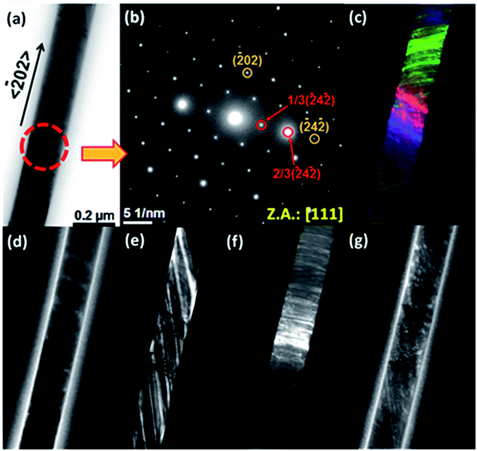 | ||
Fig. 2 (a) Bright-field TEM image of a Ni NW with monocrystalline-like properties. (b) SAED pattern obtained from the area highlighted by a red circle in panel (a), which consists of spots that can be indexed to the [111] zone axis. Spots ascribed to forbidden reflections can also be observed (they are highlighted by red arrows and circles). (c) False-color dark-field TEM image obtained from the sum of the images of panels (d)–(g). Dark-field images were obtained using the following reflections: (d) 1/3(4), (e) 2/3(4), (f) (22![[4 with combining macron]](https://www.rsc.org/images/entities/char_0034_0304.gif) ), and (g) (02). ), and (g) (02). | ||
The occurrence of forbidden reflections in nanostructured materials has been ascribed to the presence of different types of crystal defects such as dislocations,58 parallel twinning planes and (111) stacking faults,59 and/or to the low dimensionality of these materials (when they are constituted by only a reduced number of cell units) and the physical principles on which the SAED measurements are based.60 In this context, to explain the appearance of these reflections in the SAED patterns, it is very useful to introduce the concept of the Ewald sphere, which is the sphere constructed in the reciprocal space-centered in the origin of the reciprocal lattice and with radius of 1/λ, where λ is the wavelength of the incident radiation. The Bragg's condition is strictly satisfied when the surface of this sphere intersects with a reciprocal lattice point.61 However, the kinematical theory of electron diffraction predicts that in very thin crystals with few unit cells in their thickness, some diffraction signal can be detected from the reciprocal lattice points located in the proximity of the Ewald sphere instead of the Bragg condition not being exactly satisfied.61
This relaxation of the diffraction condition is manifested in the reciprocal space as an elongation of the reciprocal lattice points, whose length is inversely proportional to the crystal thickness, where their axes lie along the direction in which the specimen is more reduced. Therefore, some of these elongated points can be touched by the Ewald sphere surface even when the Bragg condition is not exactly satisfied.60,61 In this fashion, reflections of the first-order Laue zone (FOLZ) can be projected onto the zero-order Laue zone (ZOLZ) parallel to the direction in which the specimen is shortened, and they can appear in the diffraction patterns as forbidden spots.60 Note that the presence of (111) stacking faults in the fcc structures produce the elongation of the reciprocal lattice points along the [111] direction; therefore, these crystal defects favor the appearance of forbidden reflections in certain zone axes. In concrete, these reflections are observed as 1/3{224} and 2/3{224} reflections in the [111] zone axis, and 1/2{113} reflections in the [211] zone axis for fcc crystalline phase nanostructured materials.60,62,63
In our case, the observation of forbidden reflections cannot be only attributed to finite-sized effects because the Ni nanowires studied herein are not particularly thin (they have diameters of around 200 nm). Therefore, we attributed the observation of 1/3{4} and 2/3{4} forbidden reflections to a rather imperfect crystalline structure, with high density of {111} stacking faults and the formation of parallel twins. To observe these crystalline defects that originated from the forbidden reflections in the [111] axis zone by TEM, the electron beam has to be oriented in the 〈110〉 direction,63,64 which is the direction of nanowire growth in our case.
To corroborate the abovementioned hypothesis, TEM analysis was carried out viewing the NWs along the 〈110〉 direction. For this purpose, free-standing single Ni NWs were embedded into a polymeric resin and were sliced using an ultramicrotome to investigate the microstructure on the top end of the Ni NWs. Fig. 3a shows the TEM image of the top end of a single Ni nanowire sectioned using an ultramicrotome.
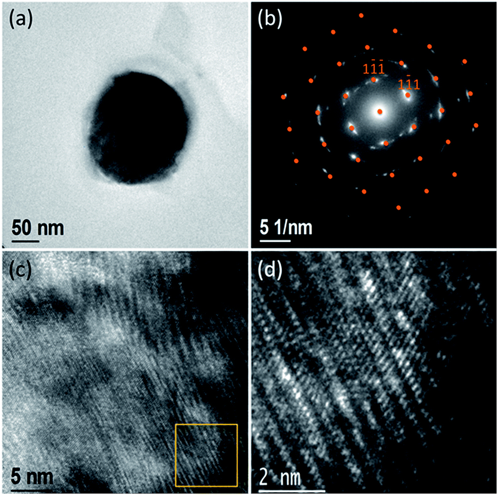 | ||
| Fig. 3 TEM images of the head-end of a Ni nanowire cross-sectioned using an ultramicrotome: (a) CTEM image. (b) SAED pattern. The orange dots indicate the positions of the diffraction spots ascribed to the [110] zone axis. (c) HRTEM image. (d) High-magnification image of the area of panel (c) marked by a yellow square. | ||
The rather circular shape of this section corroborates the cylindrical morphology of the NWs in contrast to the faceted morphology observed in single-crystal NWs obtained by template-free synthesis,65 having a diameter of around 200 nm and a surface layer of SiO2 with a thickness of around 2 nm. The SAED pattern of this section (Fig. 3b) displays bright diffraction streaks centered in positions ascribed to the zone axis [110] (highlighted with orange dots), indicating that the nanowire is not a perfect single crystal: the appearance of streaks provides evidence for the presence of stacking faults. Fig. 3c and d depict HRTEM images of the sectioned NW displayed in Fig. 3a. In these images, a dense distribution of stacking faults is clearly observed, as was expected, which is in agreement with the abovementioned discussion. These crystal defects were probably produced by the characteristics of the material growth through the electrodeposition technique and the transverse microstresses originating from the confined growth of the NWs in the cylindrical pores of the alumina membrane, therefore forcing the nanowires to crystallize in the cylindrical geometry of the membrane pores. The natural formation of crystal facets became frustrated, and the rates of crystal growth for different crystal directions were disturbed and governed by the confinement in the cylindrical-shaped nanopores of the alumina template. Consequently, the {111} stacking faults and oriented distortions of the NW crystalline lattice were observed.
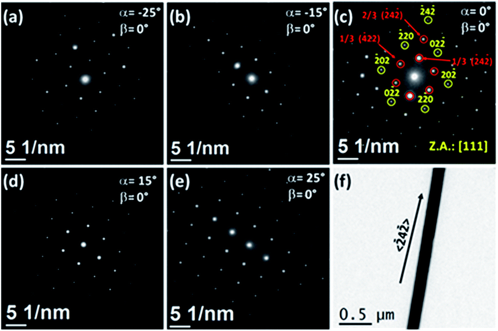
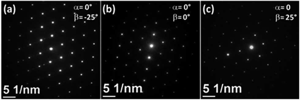
Another astonishing feature of the SAED patterns of the second family of Ni nanowires is that they changed very little with the variation of the sample tilt angles, α (Fig. 4) or β (Fig. 5), and in contrast to bulk crystals, patterns of different zone axes were not observed as the α or β tilt was varied. In this manner, the angles between the diffraction spots with respect to the pattern center almost do not change with the variation of the tilt angle α from −25° to +25° and fixing β = 0° (Fig. 4), or the variation of the tilt angle β from −25° up to +25° and fixing α = 0° (Fig. 5). However, in both the cases, the distance of the diffraction spots to the pattern center varied as the sample was tilted, displaying different tendencies for different spots. The calculated d-spacing values were considerably different than expected, with variations up to 14%, as shown in Fig. 6. These variations lead to deformed patterns at certain tilt angles that can be unrecognizable for a fcc nickel single-crystal.
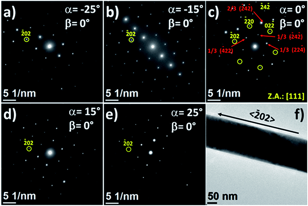 | ||
| Fig. 4 (a)–(e) SAED patterns of a Ni nanowire obtained at different tilt angles in the X axis (different tilt angle α). For all the cases, the angle β (the rotation angle in the Y axis) was fixed to zero (β = 0°). (f) TEM image of the studied Ni nanowire area. | ||
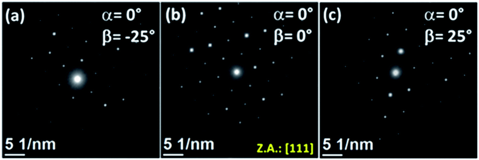 | ||
| Fig. 5 SAED patterns of a Ni nanowire obtained at different tilt angles β, but with α = 0°. | ||
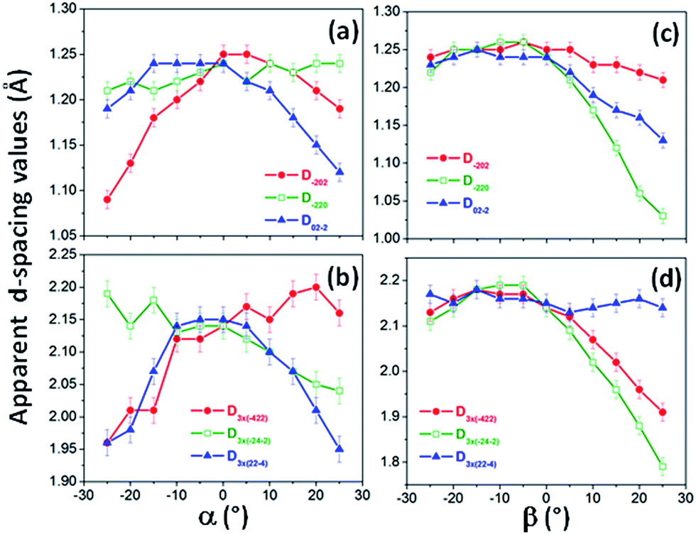 | ||
| Fig. 6 Apparent interplanar distances extracted from the diffraction spots of (a) some classically allowed reflections; (b) some forbidden reflections of the single pseudo-monocrystalline Ni nanowire studied in Fig. 4 and 5, obtained at different tilting angles α and keeping β = 0°; (c) classically allowed reflections and (d) forbidden reflections of SAED patterns obtained for the single pseudo-monocrystalline Ni nanowire studied in Fig. 4 and 5, obtained at different tilting angles β and keeping α = 0°. | ||
These facts could be explained by invoking strong oriented deformations in the nanowire crystal lattice; however, it is not the only reason allowing the observation of the dependence of the apparent d-spacing of the same crystalline planes with the sample tilt angles. In fact, these dependencies can be partly attributed to the peculiarities of the characterization technique itself, which are usually not considered in the study of the microcrystalline properties of single-crystalline nanomaterials. In this respect, Malm and O'Keefe66 demonstrated, using simulated HRTEM images of a perfect nanocrystal, that the lattice spacing directly measured from HRTEM images can deviate from the real values when the sample is tilted away from a zone-axis (up to 10%). This effect has been experimentally observed in the HRTEM images of silicon nanowires.67 Therefore, the viewing direction has to be accurately determined and considered in the analysis of the HRTEM images to correctly estimate the lattice spacing values,66 which is more complex than the estimation of d-spacings from the experimental HRTEM images measured when a single-crystal is not observed along an axis zone. In agreement with these facts and given the relationship between real and reciprocal spaces, variations in the distance of the diffraction spots to the center of the pattern when the sample is tilted away from a zone-axis should be expected, and a distorted SAED pattern with respect to the pattern measured in the initial zone-axis is observed.67
The nanowire growth by electrodeposition inside the nanopores of the alumina template is limited by diffusive mass transport and subjected to the restrictions of the pore size and geometry, in contrast to free-templated nanowires.68 The results of the second family of Ni NWs studied herein suggest that Ni NWs tend to grow with (111) surfaces in the radial directions, which are the surfaces that exhibit the lowest surface energy for the fcc metals;69 however, the crystal growth confined within the cylindrical volume of the PAAM channels could yield the frustrated formation of stable facets and right angles in these directions and (111) stacking faults occur. Therefore, the NWs were not viewed along a crystallographic direction when they were tilted from the [111] zone axis in large tilting angle ranges (we explored ranges from −25 to +25 for α and β).
This fact was also corroborated after observing the Kikuchi lines by increasing the intensity of the electron beam. In the explored tilt angle ranges, the incident electron beam did not reach the points at which the Kikuchi lines converged, which were associated with zone axes.70 On the other hand, the points of the reciprocal lattice space were rather elongated due to the occurrence of stacking faults and can intercept the Ewald sphere even at large angles away from a zone axis. This fact led to diffraction spots in the SAED patterns, with unusual dependences on the abovementioned tilting angles.
4.2 Microstructural studies of cobalt NWs
Cobalt NWs displayed SAED patterns with pseudo-monocrystalline properties very similar to those observed in the second family of Ni NWs. Fig. 7a–e show the SAED patterns obtained for a single cobalt NW (whose TEM image is presented in Fig. 7f) at different α tilt angles with β = 0°. Interestingly, the SAED pattern measured at α = 0° and β = 0° displayed a similar diffraction pattern to that of the pseudo-monocrystalline Ni NWs that can be indexed to the [111] zone axis of the fcc metallic cobalt, but with the 〈2〉 direction roughly along the long axis of the nanowire. In addition, the same 1/3{224} and 2/3{224} forbidden reflections were observed. Although the stable phase for bulk Co is only hexagonal close packed (hcp) at room temperature, several investigations have shown that the structure and crystallinity of the Co NWs grown on aluminium oxide templates by electrodeposition techniques strongly depend on the experimental conditions of the electrodeposition and the characteristics of the template membrane (pulsed or potentiostatic modes, pulse frequency, pore diameter, etc.), making the crystallization of fcc Co NWs71 or mixtures of fcc and hcp phases72 possible, as in our case.
 | ||
| Fig. 7 (a)–(e) SAED patterns of a Co nanowire obtained at different tilting angles, α. In all the cases, the angle β was fixed to zero (β = 0°). (f) TEM image of the studied Co nanowire. | ||
The observation of forbidden reflections indicates the presence of (111) stacking faults along the transverse directions of the Co NWs, and these crystalline defects could also promote the crystallization of the fcc phase. Moreover, in a manner similar to that of the pseudo-monocrystalline Ni NWs, the SAED patterns of Co NWs changed very little with the variation of the sample tilt (see Fig. 7 and 8), and the distance of the diffraction spots to the pattern center varied with different tendencies. This led to apparent d-spacing values that were moving away from the expected (or real) values for a fcc Co structure, according to the increase in the tilt angle of the incident electron beam with respect to the [111] zone axis (see Fig. 9). These facts indicate that the similar crystal defects found in the pseudo-monocrystalline Ni NWs are also present in the Co NWs.
 | ||
| Fig. 8 SAED patterns of a Co nanowire obtained at different tilt angles β, with α = 0°. | ||
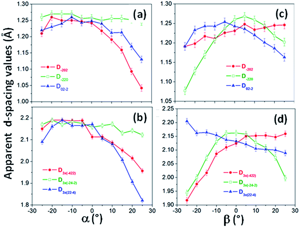 | ||
| Fig. 9 Apparent interplanar distances extracted from the diffraction spots of (a) classically allowed reflections; (b) forbidden reflections of SAED patterns obtained for the single pseudo-monocrystalline Co nanowire studied in Fig. 7 and 8, obtained at different tilting angles α, but keeping β = 0°; (c) classically allowed reflections; (d) forbidden reflections of SAED patterns obtained for the single pseudo-monocrystalline Co nanowire studied in Fig. 7 and 8, obtained at different tilting angles β, while keeping α = 0°. | ||
4.3 Microstructural studies of the multisegmented Co58Ni42/Co83Ni17 nanowires
Both NW systems studied in the previous sections exhibited fcc structures with stacking faults and inhibited crystallographic directions and planes that have been tentatively ascribed to spatial confined effects. To perform a similar study on the crystalline properties of cylindrical NWs having other crystalline structures, we synthesized and characterized multisegmented Co58Ni42/Co83Ni17 NWs, whose segments crystallized with a hcp phase and monocrystalline-like properties, in agreement with preliminary studies.28 Fig. 10 shows a typical STEM-HAADF image of one of these multisegmented NWs, together with chemical mappings based on STEM-EDS. The multisegmented character of the NW is clearly evidenced, together with the chemical compositional analysis for each CoNi segment of the NW.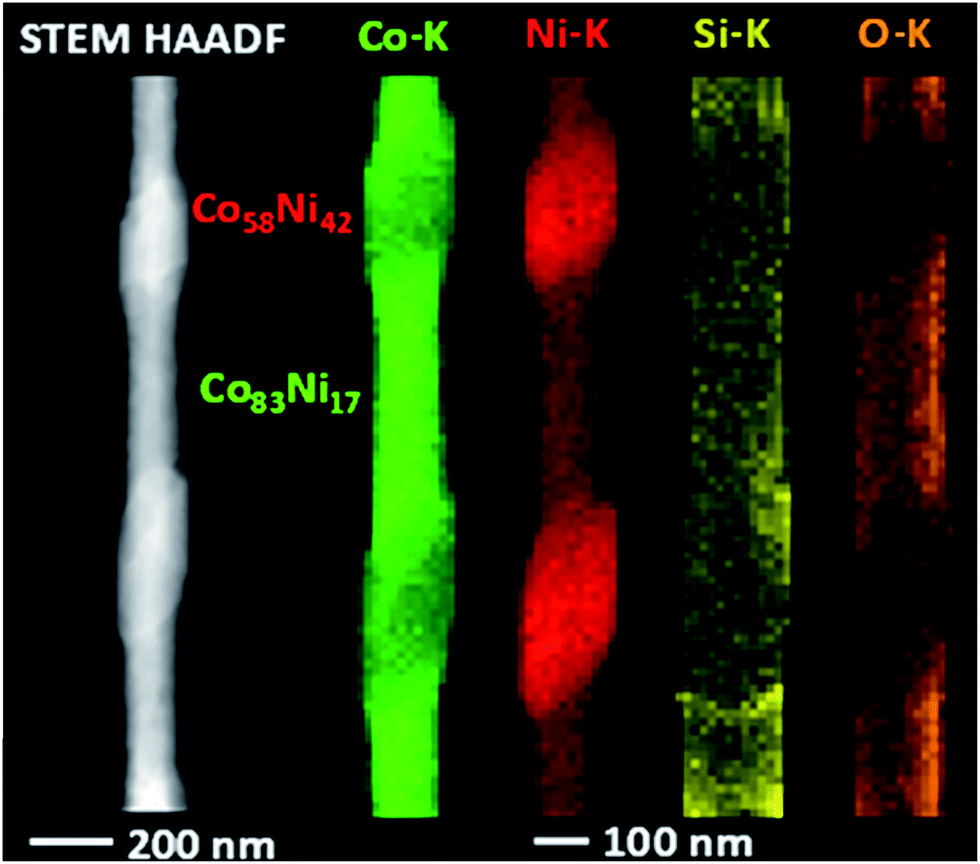 | ||
| Fig. 10 STEM-HAADF image and STEM-EDS chemical analysis mappings for a Co58Ni42/Co83Ni17 multisegmented nanowire. | ||
Fig. 11a–e depict SAED patterns obtained for a Co83Ni17 segment of a multisegmented CoNi NW (Fig. 11f) obtained at different α tilt angles with β = 0°. These patterns exhibit similar features to those observed in the abovementioned NWs systems. Particularly, changes in the symmetry of the SAED patterns associated with the observation of the NW structure along different crystallographic orientations (other zone axes) were not observed as the sample was tilted. The same occurred when the tilting angle β was changed or when α and β were simultaneously varied. In fact, in the range of explored tilting angles for the studied sample, the incident electron beam did not reach the points where the Kikuchi lines intersect (see Fig. 2S ESI†). However, at certain tilt angles, the diffraction spots can be indexed to the zone axis [0−11] of a hcp phase of the CoNi alloys, with values of the apparent interplanar distance, Dhkl, close to the bulk ones (for example, at α = 0° and β = 5°, D0−1−1 ≈ D−111 ≈ 1.92 Å and D100 ≈ 2.1 Å). However, these values notoriously vary with the modification of the tilt angles, exhibiting different tendencies (see Fig. 12), and result in distorted SAED patterns unrecognizable for a CoNi single-crystal with a fcc or hcp phase.
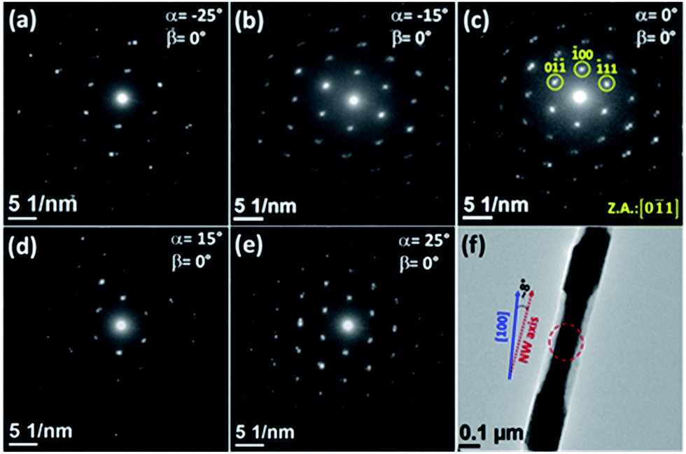 | ||
| Fig. 11 (a)–(e) SAED patterns for the Co83Ni17 segment of a Co58Ni42/Co83Ni17 multisegmented NW obtained at different tilt angles. (f) TEM image of the studied Co58Ni42/Co83Ni17 multisegmented NW. The circle highlights the segment of the NW studied in panels (a)–(e). | ||
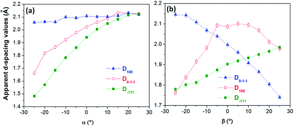 | ||
| Fig. 12 Apparent interplanar distances extracted from the diffraction spots of a Co83Ni17 segment of a Co58Ni42/Co83Ni17 multisegmented NW (studied in Fig. 11) obtained at different tilting angles (a) for α, and (b) for β. | ||
Co58Ni42 segments of the same multisegmented NW exhibited SAED patterns very similar to those observed for the Co83Ni17 segments, sharing the same structure, orientation, and features (see Fig. 3S of the ESI†).
4.4 Microstructural studies of Co73Cu27 nanowires
Fig. 4Sa of the ESI† shows TEM images of the Co73Cu27 alloyed nanowires. Studies of EDS line scans carried out along the wire axis and wire width (Fig. 4Sb–e) indicated that the Co and Cu elements were rather uniformly distributed along the entire wire. These wires grew with a hcp phase and exhibited electron diffraction properties very similar to those of the abovementioned NW systems. Fig. 13 shows SAED patterns of the same Co73Cu27 NW measured at different sample tilt angles to compare with the previous results obtained for a larger diameter and with different alloy composition for the nanowire samples. These patterns can be indexed to the zone axis [001] of a hcp phase; however, the distances of the diffraction spots to the center of the SAED pattern are dependent on the sample tilt angles, exhibiting analogous behavior to those observed in the abovementioned nanowire systems.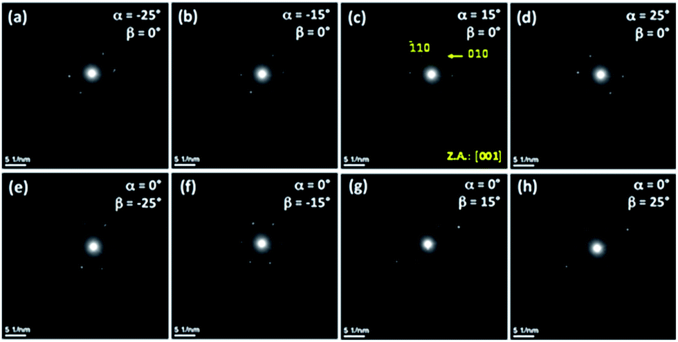 | ||
| Fig. 13 SAED patterns of a Co73Cu27 NW obtained at different tilting angles α and β. | ||
5. Conclusions
Four different cylindrical nanowire systems, grown by standard electrodeposition techniques in the nanometer size channels of porous alumina templates, were investigated using TEM and SAED. These nanowires displayed monocrystalline-like SAED patterns; however, studies performed under different NW orientations revealed electron diffraction properties that indicate that these nanowires are far from perfect single-crystals. Particularly, their SAED patterns obtained in certain specific directions were constituted by well-defined diffraction spots that did not experience apparent changes from one zone axis to another as the NW was tilted in a wide range of tilt angles. Moreover, the distance of the diffraction spots to the center of the diffraction pattern, associated with the interplanar distances, widely varied depending on the sample tilt with respect to a zone axis, showing different trends for different diffraction spots. In addition, SAED patterns of NWs with fcc structures exhibited classically forbidden reflections. These features can lead to unrecognizable SAED patterns or to their incorrect indexing and are rather general for NWs electrodeposited into PAAM template nanopores because they were observed in NWs with different compositions, diameters, and crystalline structures. These behaviors have been ascribed to the inclination of the electron beam with respect to the crystallographic direction of the material and the occurrence of stacking faults probably produced by the confined growth of the NWs in a reduced cylindrical volume. The comprehension of these effects is crucial for the entire understanding of the physical properties of 1D low-dimensional materials with cylindrical morphologies and their exploitation in a wide variety of emerging technologies based on these nanostructures.Acknowledgements
Financial support from the Secretariat of Public Education of Mexico/Secretaría de Educación Pública de México (SEP), National Council of Science and Technology of Mexico/Consejo Nacional de Ciencia y Tecnología de México (CONACYT), Spanish MINECO and Principality of Asturias from FICyT under research projects “Red Temática de Colaboración: Sistemas de Baja Dimensionalidad con Aplicaciones Biotecnológicas”, CB12-179486, MAT2013-48054-C2-2-R, MAT2016-76824-C3-3-R and FC-15-GRUPIN14-085, respectively, is acknowledged. The authors thank to M.Sc. Mónica A. Ceniceros Reyes for their technical support in the preparation and characterization of materials. Scientific-Technical Common Research Services of University of Oviedo and, particularly, the Laboratory of “Membranas Nanoporosas” of Nanotechnology Unit, are also acknowledged for their valuable technical support.References
- C. M. Lieber, MRS Bull., 2003, 28, 486 CrossRef CAS.
- Y. Cui, Z. Zhong, D. Wang, W. U. Wang and C. M. Lieber, Nano Lett., 2003, 3, 149 CrossRef CAS.
- Y. Cui, X. Duan, J. Hu and C. M. Lieber, J. Phys. Chem. B, 2000, 104, 5213 CrossRef CAS.
- Y. Cui and C. M. Lieber, Science, 2001, 291, 851 CrossRef CAS PubMed.
- Y. Huang, X. Duan, Y. Cui, L. J. Lauhon, K. H. Kim and C. M. Lieber, Report Science, 2001, 294, 1313 CrossRef CAS PubMed.
- Z. Zhong, D. Wang, Y. Cui, M. W. Bockrath and C. M. Lieber, Report Science, 2003, 302, 1377 CrossRef CAS PubMed.
- X. Duan, Y. Huang, Y. Cui, J. Wang and C. M. Lieber, Nature, 2001, 409, 66 CrossRef CAS PubMed.
- J. Wang, M. S. Gudiksen, X. Duan, Y. Cui and C. M. Lieber, Report Science, 2001, 293, 1455 CAS.
- J. García, V. Vega, L. Iglesias, V. M. Prida, B. Hernando, E. D. Barriga-Castro, R. Mendoza-Reséndez, C. Luna, D. Görlitz and K. Nielsch, Phys. Status Solidi A, 2014, 211, 1041 CrossRef.
- A. C. Niemann, T. Böhnert, A. K. Michel, S. Bäßler, B. Gotsmann, K. Neuróhr, B. Tóth, L. Péter, I. Bakonyi, V. Vega and V. M. Prida, Adv. Electron. Mater., 2016, 2, 1600058 CrossRef.
- P. Krzysteczko, X. Hu, N. Liebing, S. Sievers and H. W. Schumacher, Phys. Rev. B: Condens. Matter Mater. Phys., 2015, 92, 140405 CrossRef.
- Y. P. Ivanov, A. Chuvilin, L. G. Vivas, J. Kosel, O. Chubykalo-Fesenko and M. Vázquez, Sci. Rep., 2016, 6, 23844 CrossRef CAS PubMed.
- Y. P. Ivanov, A. Chuvilin, S. Lopatin and J. Kosel, ACS Nano, 2016, 10, 5326 CrossRef CAS PubMed.
- L. A. Rodríguez, C. Bran, D. Reyes, E. Berganza, M. Vázquez, C. Gatel, E. Etienne Snoeck and A. Asenjo, ACS Nano, 2016, 10, 9669 CrossRef PubMed.
- X. Chen and S. S. Mao, Chem. Rev., 2007, 107, 2891 CrossRef CAS PubMed.
- C. N. R. Rao, F. L. Deepak, G. Gundiah and A. Govindaraj, Prog. Solid State Chem., 2003, 31, 5 CrossRef CAS.
- C. N. R. Rao and A. Govindaraj, Adv. Mater., 2009, 21, 4208 CrossRef CAS.
- C. Luna, E. D. Barriga-Castro and R. Mendoza-Reséndez, Acta Mater., 2014, 66, 405 CrossRef CAS.
- The chemistry of nanomaterials: synthesis, properties and applications, ed. C. N. R. Rao, A. Müller and A. K. Cheetham, John Wiley & Sons. 2006 Search PubMed.
- R. Mendoza-Reséndez, C. Luna, E. D. Barriga-Castro, P. Bonville and C. J. Serna, Nanotechnology, 2012, 23, 225601 CrossRef PubMed.
- A. Huczko, Appl. Phys. A: Mater. Sci. Process., 2000, 70, 365 CrossRef CAS.
- B. Folch, Y. Guari, J. Larionova, C. Luna, C. Sangregorio, C. Innocenti, A. Caneschi and C. Guérin, New J. Chem., 2008, 32, 273 RSC.
- J. Joo, K. T. Park, B. H. Kim, M. S. Kim, S. Y. Lee, C. K. Jeong, J. K. Lee, D. H. Park, W. K. Yi, S. H. Lee and K. S. Ryu, Synth. Met., 2003, 135, 7 CrossRef.
- V. M. Prida, J. García, B. Hernando, C. Bran, L. G. Vivas and M. Vázquez, Electrochemical Synthesis of Magnetic Nanowires with Controlled Geometry and Magnetic Anisotropy, in Magnetic Nano- and Microwires: Design, Synthesis, Properties and Applications Part I: Design and synthesis of magnetic nano- and microwires, Woodhead Publishing, Elsevier, 2015, ch. 02, p. 41 Search PubMed.
- M. Vázquez, K. Pirota, M. Hernández-Vélez, V. M. Prida, D. Navas, R. Sanz, F. Batallán and J. Velázquez, J. Appl. Phys., 2004, 95, 6642 CrossRef.
- W. Lee, R. Ji, U. Gösele and K. Nielsch, Nat. Mater., 2006, 5, 741 CrossRef CAS PubMed.
- S. Talapatra, X. Tang, M. Padi, T. Kim, R. Vajtai, G. V. S. Sastry, M. Shima, S. C. Deevi and P. M. Ajayan, J. Mater. Sci., 2009, 44, 2271 CrossRef CAS.
- H. Schlörb, V. Haehnel, M. S. Khatri, A. Srivastav, A. Kumar, L. Schultz and S. Fähler, Phys. Status Solidi B, 2010, 247, 2364 CrossRef.
- V. M. Prida, J. García, L. Iglesias, V. Vega, D. Görlitz, K. Nielsch, E. D. Barriga-Castro, R. Mendoza-Reséndez, A. Ponce and C. Luna, Nanoscale Res. Lett., 2013, 8, 263 CrossRef PubMed.
- C. T. Sousa, D. C. Leitao, M. P. Proenca, J. Ventura, A. M. Pereira and J. P. Araujo, Nanoporous alumina as templates for multifunctional applications, Appl. Phys. Rev., 2014, 1, 031102 Search PubMed.
- A. Fert and L. Piraux, J. Magn. Magn. Mater., 1999, 200, 338 CrossRef CAS.
- J. Cantu-Valle, E. D. Barriga-Castro, V. Vega, J. García, R. Mendoza-Reséndez, C. Luna, V. M. Prida, K. Nielsch, F. Mendoza-Santoyo, M. J. Yacaman and A. Ponce, J. Magn. Magn. Mater., 2015, 379, 294 CrossRef CAS.
- V. M. Prida, K. R. Pirota, D. Navas, A. Asenjo, M. Hernández-Vélez and M. Vázquez, J. Nanosci. Nanotechnol., 2007, 7, 272 CAS.
- A. K. Srivastav and R. Shekhar, J. Magn. Magn. Mater., 2014, 349, 21 CrossRef CAS.
- A. Fernández-Pacheco, L. Serrano-Ramón, J. M. Michalik, M. R. Ibarra, J. M. De Teresa, L. O'Brien, D. Petit, J. Lee and R. P. Cowburn, Sci. Rep., 2013, 3, 1492 Search PubMed.
- S. Aravamudhan, J. Singleton, P. A. Goddard and S. Bhansali, J. Phys. D: Appl. Phys., 2009, 42, 115008 CrossRef.
- A. Ramazani, M. A. Kashi, M. Alikhani and S. Erfanifam, J. Phys. D: Appl. Phys., 2007, 40, 5533 CrossRef CAS.
- K. Maaz, S. Karim, M. Usman, A. Mumtaz, J. Liu, J. L. Duan and M. Maqbool, Nanoscale Res. Lett., 2010, 5, 1111 CrossRef CAS PubMed.
- N. J. Gerein and J. A. Haber, J. Phys. Chem. B, 2005, 109, 17372 CrossRef CAS PubMed.
- K. O. Moura, L. A. S. De Oliveira, P. F. S. Rosa, C. B. R. Jesus, M. E. Saleta, E. Granado, F. Béron, P. G. Pagliuso and K. R. Pirota, Sci. Rep., 2016, 6, 28364 CrossRef CAS PubMed.
- L. A. S. De Oliveira and K. R. Pirota, Mater. Res. Bull., 2013, 48, 1593 CrossRef CAS.
- X. Liu, J. Liu, L. Y. Antipina, J. Hu, C. Yue, A. M. Sanchez, P. B. Sorokin, Z. Mao and J. Wei, Nano Lett., 2016, 16(10), 6188 CrossRef CAS PubMed.
- J. García, V. M. Prida, L. G. Vivas, B. Hernando, E. D. Barriga-Castro, R. Mendoza-Reséndez, C. Luna, J. Escrig and M. Vázquez, J. Mater. Chem. C, 2015, 3, 4688 RSC.
- J. H. Lee, J. H. Wu, H. L. Liu, J. U. Cho, M. K. Cho, B. H. An, J. H. Min, S. J. Noh and Y. K. Kim, Angew. Chem., Int. Ed., 2007, 46, 3663 CrossRef CAS PubMed.
- L. Clime, S. Y. Zhao, P. Chen, F. Normandin, H. Roberge and T. Veres, Nanotechnology, 2007, 18, 435709 CrossRef.
- Z. Yu-Cheng, H. Chun-Lian and Z. Yan-Fang, Appl. Phys. A: Mater. Sci. Process., 2015, 121, 297 CrossRef.
- E. M. Palmero, C. Bran, R. P. del Real and M. Vázquez, Nanotechnology, 2015, 26, 461001 CrossRef PubMed.
- A. Santos, J. M. Montero-Moreno, J. Bachmann, K. Nielsch, P. Formentín, J. Ferré-Borrull, J. Pallares and L. F. Marsal, ACS Appl. Mater. Interfaces, 2011, 3, 1925 CAS.
- V. Vega, T. Böhnert, S. Martens, M. Waleczek, J. M. Montero-Moreno, D. Görlitz, V. M. Prida and K. Nielsch, Nanotechnology, 2012, 23, 465709 CrossRef CAS PubMed.
- V. Vega, J. García, J. M. Montero-Moreno, B. Hernando, J. Bachmann, V. M. Prida and K. Nielsch, ACS Appl. Mater. Interfaces, 2015, 7, 28682 CAS.
- V. Romero, V. Vega, J. García, R. Zierold, K. Nielsch, V. M. Prida, B. Hernando and J. Benavente, ACS Appl. Mater. Interfaces, 2013, 5, 3556 CAS.
- E. Gómez, J. Ramirez and E. Vallés, J. Appl. Electrochem., 1998, 28, 71 CrossRef.
- E. Gómez, S. Pané and E. Vallés, Electrochim. Acta, 2005, 51, 146 CrossRef.
- A. Ghahremaninezhad and A. Dolati, J. Alloys Compd., 2009, 480, 275 CrossRef CAS.
- L. Tian, J. Ramirez and E. Vallés, J. Appl. Electrochem., 2011, 28, 71 Search PubMed.
- A. Cortés, R. Lavín, J. C. Denardin, R. E. Marotti, E. A. Dalchiele, P. Valdivia and H. Gómez, J. Nanosci. Nanotechnol., 2011, 11, 3899 CrossRef.
- G. Ali and M. Maqbool, Nanoscale Res. Lett., 2013, 8, 352 CrossRef PubMed.
- L. Lu, A. Kobayashi, Y. Kikkawa, K. Tawa and Y. Ozaki, J. Phys. Chem. B, 2006, 110, 23234 CrossRef CAS PubMed.
- V. Germain, J. Li, D. Ingert, Z. L. Wang and M. P. Pileni, J. Phys. Chem. B, 2003, 107, 8717 CrossRef CAS.
- J. Reyes-Gasga, A. Gómez-Rodríguez, X. Gao and M. J. Yacamán, Ultramicroscopy, 2008, 108(9), 929 CrossRef CAS PubMed.
- P. J. Goodhew, J. Humphreys and R. Beanland, Electron Microscopy and Analysis, Taylor & Francis Inc, London and New York, 3rd edn, 2001 Search PubMed.
- H. Alexander, J. C. H. Spence, D. Shindo, H. Gottschalk and N. Long, Philos. Mag. A, 1986, 53, 627 CrossRef CAS.
- R. Mendoza-Reséndez, N. O. Núñez, E. D. Barriga-Castro and C. Luna, RSC Adv., 2013, 3, 20765 RSC.
- F. M. Davidson, D. C. Lee, D. D. Fanfair and B. A. Korgel, J. Phys. Chem. C, 2007, 111, 2929 CAS.
- L. Qin, J. Xu, X. Dong, Q. Pan, Z. Cheng, Q. Xiang and F. Li, Nanotechnology, 2008, 19, 185705 CrossRef PubMed.
- J. O. Malm and M. A. O'Keefe, Ultramicroscopy, 1997, 68, 13 CrossRef CAS.
- D. C. Bell, Y. Wu, C. J. Barrelet, S. Gradečak, J. Xiang, B. P. Timko and C. M. Lieber, Microsc. Res. Tech., 2004, 64, 373 CrossRef PubMed.
- L. J. Brogan and A. M. Stacy, Mater. Lett., 2010, 64, 1674 CrossRef CAS.
- J. M. Zhang, F. Ma and K. W. Xu, Appl. Surf. Sci., 2004, 229, 34 CrossRef CAS.
- E. Levine, W. L. Bell and G. Thomas, J. Appl. Phys., 1966, 37, 2141 CrossRef CAS.
- Z. Jun, A. J. Grenville, H. S. Tiehan, E. D. Steve and L. Guanghai, J. Appl. Phys., 2007, 101, 054310 CrossRef.
- V. Scarani, B. Doudin and J. P. Ansermet, J. Magn. Magn. Mater., 1999, 205, 241 CrossRef CAS.
Footnote |
| † Electronic supplementary information (ESI) available. See DOI: 10.1039/c7ra00691h |
| This journal is © The Royal Society of Chemistry 2017 |