
 Open Access Article
 This Open Access Article is licensed under a
 Creative Commons Attribution 3.0 Unported Licence
New insight into strong correlated states realised in a ferroelectric and paraelectric chalcogenide Sn2P2S6 crystal
T. Babukaab,
K. Glukhov b,
Y. Vysochanskiib and
M. Makowska-Janusik*a
b,
Y. Vysochanskiib and
M. Makowska-Janusik*a
aInstitute of Physics, Faculty of Mathematics and Natural Science, Jan Dlugosz University in Czestochowa, Al. Armii Krajowej 13/5, 42200 Czestochowa, Poland. E-mail: m.makowska@ajd.czest.pl
bInstitute for Solid State Physics and Chemistry, Uzhgorod National University, Voloshyn Street 54, Uzhgorod 88000, Ukraine
First published on 24th May 2017
Abstract
In the present study, the electronic properties of both ferroelectric and paraelectric phases of the Sn2P2S6 (SPS) chalcogenide crystal were investigated using first principles methods. Via applying the density functional theory methodology (DFT) with different functionals, their energy band structures were calculated and discussed. It was confirmed that the pure DFT methodology as well as that extended by the hybrid functionals did not provide a satisfactory result in the prediction of the electronic parameters of the SPS crystals. To improve the theoretical modelling of the abovementioned materials, the Hubbard correction was proposed in this study, and as a consequence, the appropriate electronic parameters were obtained. The correct values of the band gap for the para- and ferroelectric phases of the SPS were obtained by applying the Hubbard parameters for the p orbitals of the S and P atoms. Moreover, the influence of the Hubbard parameters on the charge transfer between atoms was shown and analyzed. In this case, the electronic character of the (SP3) subsystem was explained and the role of the Sn atoms in the investigated chalcogenide systems was described.
Introduction
The design and discovery of modern materials are based on the prediction of the structures and properties of both real and hypothetical substances. The combination between synthesis, characterisation of the physical and chemical properties, as well as material engineering is complex to study the existing and newly created materials. Adding a component obtained from theoretical research could further strengthen the identification of new systems. Therefore, theoretical investigations supported by experimental measurements can enhance essential contribution in the material design process.The present study was focused on the theoretical investigations of the chalcogenide crystals1 belonging to the material group M2P2X6, where M is a transition metal or post-transition metal and X = S or Se atom. These materials crystallize in the monoclinic symmetry and show a layered structure. The tin-thiohypodiphosphate Sn2P2S6 (SPS) crystal, belonging to the abovementioned group, is photosensitive in the red and near-infrared spectral region with good photorefractivity2–5 as well as has fine photovoltaic,6 electrooptic,7 and piezoelectric8 characteristics. Its diagonal electro-optical coefficient r111 is equal to 166 pm V−1 at λ = 1313 nm.7 The SPS crystal is also interesting for nonlinear optical applications in the visible and near infrared wavelength range.9 Its second-order phase transition from the noncentrosymmetric ferroelectric (FE) to the centrosymmetric paraelectric (PE) phase occurs at the Curie temperature TC = 338 K.10 The SPS crystal exhibits negative thermal expansion caused by the Sn5s–S3p interactions.11 Contrary to the most industrially relevant ferroelectrics, which are insulators, the SPS crystal at room temperature shows pronounced semiconducting features (Eg = 2.3 eV).12 Moreover, increase in the applied pressure changes the electronic properties of the SPS crystal. Electronic transport measurements have shown that the band gap of the SPS crystal dramatically decreases down to 0.3 eV at 20 GPa. Additionally, rapid shrinkage of the electrical resistance with the increasing pressure up to 39 GPa indicates a possibility of sample metallization at the same pressure point.13 Doping of the Sn2P2S6 crystal by Te, Sb, Bi, and Pb atoms substantially modifies its electronic parameters.14–16 All the abovementioned properties make the SPS crystal a promising material for different industrial applications. However, further progress in crystal elaboration requires a better understanding of its parameters. The physical and chemical properties of the SPS single crystal have been experimentally2,6–8,11,17–24 as well as theoretically11,25–28 studied. The energy band structures of both the FE and PE phases were investigated via the first principle calculations using the DFT methodology. The local density approximation LDA26 applied to the performed calculations does not provide satisfactory results. This is because the SPS crystal represents a class of strongly correlated electron system and thus the electron interaction effect should be taken into account. Generally, pure LDA as well as the generalized gradient approximation (GGA) are not appropriate for studying strongly correlated systems, and thus, the Hubbard approximation should be applied. Additionally, investigation of the atomic charge redistribution and the interatomic distances changing under the variation of the Hubbard parameter values are the first steps to explain the bonds peculiarities in chalcogenides.
In the present study, the DFT-based calculations of the electronic and structural properties of both the FE and PE phases of the SPS single crystal were performed by applying the Hubbard approximation. The implemented approach was based on the development of the effective Hubbard-like Hamiltonian depending on the set of parameters.29 Qualitative and quantitative descriptions of the abovementioned systems can be made when proper Hubbard parameters are obtained. They can be predicted theoretically or via experimental measurements. To the best of our knowledge, the present study proposes for the first time a theoretical analysis of the electronic and structural properties of the SPS crystal in both phases using the Hubbard approximation. The unknown Hubbard parameters were theoretically predicted. As the correctness criterion for the theoretical calculations, the compatibility of the output data with the experimentally obtained results was investigated. Theoretically predicted data were compared to the adequate experimentally measured physical parameters, and the Hubbard parameters were self-consistently corrected.
Crystallographic parameters of the SPS crystal
At room temperature, the SPS crystal is in the FE state and has a low-symmetry structure of the monoclinic system (space group Pn, no. 7) as compared to that in the PE phase (P21/n, no. 14), which is centrosymmetric.30 In Table 1, the lattice parameters of both the FE and PE phases of the SPS crystal are presented.31,32 The fractional positions for the representative atoms of both structures were obtained and are presented in Table 2.31,32 The unit cells of the PE and the FE-Sn2P2S6 structures are shown in Fig. 1. By analyzing the atomic positions of these two lattices, it can be observed that the main difference between the FE and PE phases originates from the arrangement of the Sn atoms in the unit cell. Below the TC, the Sn atoms are significantly shifted in the [100] direction with respect to the location in the PE centrosymmetric state. Moreover, two non-equivalent Sn1 and Sn2 atoms are shifted by 0.325 Å along a, 0.044 Å along b, and 0.094 Å along the c direction and by 0.225 Å along a, 0.044 Å along b, and 0.033 Å along the c direction, respectively. Changes in the position of the P and S atoms below and above the TC are insignificant. Thus, it can be concluded that the Sn atoms make the discussed sublattice ferroactive.11,26 With the aim of providing future description of the changes in the chemical bond lengths, the visualization of the initial values of the interatomic distances in the FE and PE phases are presented in Fig. 2. The bonds between the nearest neighbours in the [P2S6] anion complexes and in the [SnS8] polyhedrons are marked by red, the second nearest neighbours are depicted by green, and all the other atoms are linked via orange-colored bonds.| Parameters | FE – Sn2P2S6 | PE – Sn2P2S6 |
|---|---|---|
| a, Å | 9.378(5) | 9.362(2) |
| b, Å | 7.488(5) | 7.493(1) |
| c, Å | 6.513(5) | 6.550(3) |
| β, ° | 91.15(5) | 91.17(3) |
| Space group | Pn | P21/n |
| Atom name | x | y | z |
|---|---|---|---|
| FE – Sn2P2S6 | |||
| Sn1 | 0.5270(2) | 0.3856(2) | 0.7224(4) |
| Sn2 | 0.0279(2) | 0.1245(2) | 0.7870(2) |
| P1 | 0.6836(4) | 0.8608(5) | 0.8108(7) |
| P2 | 0.8174(4) | 0.6447(7) | 0.6908(7) |
| S1 | 0.4898(4) | 0.7511(7) | 0.8491(7) |
| S2 | 0.7788(4) | 0.9462(7) | 0.0750(7) |
| S3 | 0.6942(4) | 0.0517(5) | 0.5921(7) |
| S4 | 0.0149(4) | 0.7437(7) | 0.6497(7) |
| S5 | 0.7147(4) | 0.5633(4) | 0.4288(7) |
| S6 | 0.8050(4) | 0.4480(7) | 0.9025(7) |
![[thin space (1/6-em)]](https://www.rsc.org/images/entities/char_2009.gif) |
|||
| PE – Sn2P2S6 | |||
| Sn1 | 0.24310(10) | 0.36920(10) | −0.04110(10) |
| P1 | 0.0671(2) | 0.3914(2) | 0.4394(4) |
| S1 | 0.2629(2) | 0.4975(2) | 0.3991(4) |
| S2 | −0.0328(2) | 0.3090(2) | 0.1772(4) |
| S3 | 0.0570(2) | 0.1976(2) | 0.6558(4) |
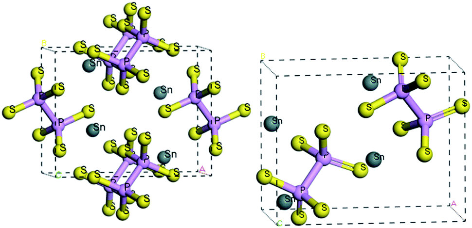 | ||
| Fig. 1 The unit cell of the PE-Sn2P2S6 (left) and FE-Sn2P2S6 (right) structure. | ||
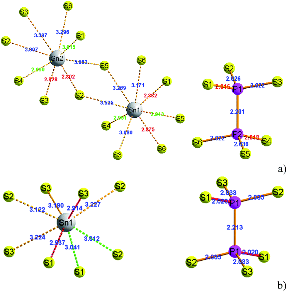 | ||
| Fig. 2 The [SnS8] polyhedrons and [P2S6] anion complexes with experimentally specified distances between atoms in the FE (a) and PE-Sn2P2S6 (b) structures.31,32 | ||
Computational methodology
Theoretical approach
The DFT theory is a first-principles quantum-chemical technique formulated by Hohenberg, Kohn, and Sham in 1964 (ref. 33 and 34) and is based on two main approximations: LDA34 and GGA.35,36 The electronic properties of different chalcogenide crystals were calculated using LDA,26,37 GGA/PBE, and hybrid HSE06 (ref. 38) functionals. In the cited studies, it has been shown that the valence band energy level is rather stable, whereas the conduction band energy is evaluated depending on the used functional. However, the LDA approximation does not provide good results via the study of the energy band structure of the SPS crystal.37 Because the studied crystal was characterized via partially covalent bonds, more developed DFT functionals were needed to characterise its electronic properties. In some cases, realistic energy band structures of the semiconductors can be obtained using the GW functional.39 Moreover, range-separated hybrid functionals were successfully used to perform calculations of the polarizabilities,40,41 predict the charge-transfer and Rydberg excitations,42 or estimate the nonlinear optical properties,43 noticed as the phenomenon arising from the heterogeneous electron density distribution. The range-separated functionals agreed well with the calculations performed for the semiconducting TiO2 nanostructures, where the electrons were localized around the nuclei and the interatomic bonds had a more ionic character.44 In the case of the semiconducting SPS crystal, the electrons are shared more between atoms, suggesting that the range-separated functionals will not provide satisfactory results for the calculations of the electronic properties. In our previous study45 describing the properties of the NiTiO3 nanocrystals, it was shown that the application of the Hubbard Hamiltonian provided better results than the used hybrid functionals. This may be because of the regularity in the case of the crystals having strongly correlated electrons.The DFT methodology augmented by the Hubbard parameters (DFT+U) was introduced by Anisimov et al.46–48 In this model, a correction of the localized states in the LDA approximation is implemented and the DFT energy functional is extended using the Hubbard parameters as follows:
 | (1) |
It was shown that the calculated band gap value and the lattice parameters of the semiconductors using the DFT+U method instead of the semilocal functional may be comparable to the experimentally. On changing the correlation energy U and the energy-level separation, the system undergoes a transition between the ionic and the Mott insulating phase.49 Therefore, in the present study, the importance of the electron–electron interaction on the electron-lattice coupling has been demonstrated. A strong lattice effect caused by the electron correlation may be significant for the origin of the displacement-type ferroelectricity and high-TC superconductivity. The extended Hubbard correction is able to significantly improve the description of the SPS semiconductor with respect to the GGA approximation, providing a more accurate estimation of the structural and electronic properties.
Computational details
In the present study, the influence of the strong correlated electron subsystem on the electronic properties of the SPS single crystals was investigated and discussed. In this case, the CASTEP program50 (module of the Materials Studio package) was used for performing the quantum-chemical calculations. The abovementioned program is based on the total energy plane-wave pseudopotential method.First, the geometry of the investigated structure was optimized with respect to the total energy minimization within the Broyden–Fletcher–Goldfarb–Shanno (BFGS) algorithm.51 During the geometry optimization procedure, the size of the unit cell and its symmetry were kept constant. The convergence criteria for the optimization procedure were chosen as follows: the convergence accuracy for the total energy during the geometry optimization procedure was equal to 2 × 10⁻⁵ eV per atom, the force on the atom was less than 0.01 eV Å−1, the stress on the atom was not more than 0.02 GPa, and the maximal atomic displacement was equal to 2 × 10⁻³ Å. The electronic exchange-correlation energy was treated within the frame of the LDA,34 GGA/PBE,36 HSE06,52 and GGA/PBE+U46 functionals. The ultrasoft pseudopotential has been used in the calculations.53 Pseudoatomic calculations were performed for the P 3s23p3, S 3s23p4, and Sn 5s25p2 electronic configurations. The plane-wave set was restricted by the cut-off energy equal to 400 eV. The integration over the Brillouin zone was performed by partitioning the 4 × 5 × 6 grid with a shift from the origin of the coordinates according to the Monkhorst–Pack scheme. The total energy convergence criterion was speculated to be fulfilled when the self-consistent field (SCF) tolerance was equal to 10−5 eV per atom. The abovementioned computational parameters were also applied to perform the electronic properties calculations.
Results and discussion
Structural properties of the Sn2P2S6 crystal
For studying the electronic properties of the SPS single crystal, its geometry in the PE and FE phase was first optimized. The lattice parameters and the symmetry of the studied structure were kept constant. Atom positions were relaxed according to the minimum of the total energy achievement. In this way, the difference between the PE and FE phases was preserved. At zero temperature, the PE structure becomes unstable and barely distinguishable from the FE structure after full optimization. The experimentally measured interatomic distances and the corresponding interatomic distances optimized by applying the GGA/PBE and GGA/PBE+U functionals demonstrate the insignificant difference concerning the P–S and P–P bonds for both phases (see Table 3). Generally, the GGA/PBE methodology is more appropriate to experimentally reproduce the obtained data of the P–S and P–P distances. Significant differences were observed for the Sn–S bonds. They were better reproduced using the DFT/PBE+U approach; however, the abovementioned methodology was not suitable for the P–S and P–P distance calculations. It can be observed that the differences for the Sn–S distances become essentially smaller by applying the DFT/PBE+U approach instead of the DFT/PBE method as observed via the experimental data. It can be concluded that the electron interaction in the SPS crystal occurring between the Sn and S atoms is significant.| Bond identification | Bond length | Difference [%] | |||
|---|---|---|---|---|---|
| Exp. [Ǻ] | DFT/PBE [Ǻ] | DFT/PBE+U [Ǻ] | DFT/PBE | DFT/PBE+U | |
| PE – Sn2P2S6 | |||||
| P1–S1 | 2.020(3) | 2.02125 | 1.97382 | −0.06 | 2.30 |
| P1–S2 | 2.035(3) | 2.05431 | 1.98275 | −0.95 | 2.58 |
| P1–S3 | 2.033(2) | 2.02754 | 1.97147 | 0.27 | 3.0 |
| Sn1–S2 | 3.012(3) | 2.64036 | 2.89034 | 12.34 | 4.04 |
| Sn1–S3 | 2.914(3) | 2.61195 | 2.82360 | 10.37 | 3.11 |
| Sn1–S1 | 2.9372(19) | 2.74261 | 2.86801 | 6.62 | 2.35 |
| Sn1–S2 | 3.122(3) | 3.35875 | 3.21237 | −7.57 | −2.88 |
| Sn1–S3 | 3.224(3) | 3.53468 | 3.35038 | −9.56 | −3.91 |
| Sn1–S3 | 3.190(2) | 3.50726 | 3.27509 | −9.93 | −2.66 |
| Sn1–S1 | 3.041(3) | 3.22583 | 3.04822 | −7.05 | −0.43 |
| Sn1–S2 | 3.227(2) | 3.22611 | 3.20392 | 0.03 | 0.72 |
| P1–P1 | 2.213(2) | 2.21335 | 2.16702 | −0.02 | 2.08 |
|
|||||
| FE – Sn2P2S6 | |||||
| P1–S1 | 2.015(6) | 2.03418 | 1.97741 | −0.95 | 1.89 |
| P1–S2 | 2.026(6) | 2.03002 | 1.97266 | −0.20 | 2.66 |
| P1–S3 | 2.022(6) | 2.03111 | 1.97835 | −0.42 | 2.18 |
| P1–Sn2 | 3.456(5) | 3.42626 | 3.47362 | 0.86 | −0.49 |
| P1–P2 | 2.201(6) | 2.21970 | 2.16931 | −0.85 | 1.46 |
| P2–S4 | 2.018(6) | 2.00492 | 1.96830 | 0.65 | 2.49 |
| P2–S5 | 2.036(6) | 2.04827 | 1.98503 | −0.60 | 2.52 |
| P2–S6 | 2.022(7) | 2.02782 | 1.97231 | −0.29 | 2.49 |
| Sn1–S1 | 2.882(6) | 2.69923 | 2.85515 | 6.36 | 0.95 |
| Sn1–S2 | 3.525(6) | 3.76666 | 3.50991 | −6.83 | 0.44 |
| Sn1–S3 | 3.080(5) | 3.18034 | 3.08295 | −2.62 | −0.08 |
| Sn1–S4 | 2.951(6) | 2.79599 | 2.93865 | 5.27 | 0.43 |
| Sn1–S5 | 2.943(5) | 2.94589 | 2.97968 | −0.10 | −1.22 |
| Sn1–S6 | 2.875(5) | 2.60683 | 2.91847 | 9.34 | −1.49 |
| Sn2–S1 | 3.015(6) | 3.15200 | 3.03653 | −4.52 | −0.69 |
| Sn2–S2 | 2.802(5) | 2.59035 | 2.79022 | 7.57 | 0.43 |
| Sn2–S3 | 2.828(5) | 2.61781 | 2.78715 | 7.44 | 4.13 |
| Sn2–S4 | 2.990(6) | 3.18695 | 2.97835 | −6.56 | 0.40 |
| Sn2–S5 | 3.053(4) | 2.74308 | 2.99619 | 10.16 | 1.87 |
| Sn2–S6 | 3.296(6) | 3.44598 | 3.32416 | −4.53 | −0.83 |
Electronic properties of the Sn2P2S6 crystal
The electronic properties of the SPS crystal were computed via the spin-polarized approach for the primitive unit cell. The energy band structure calculations were performed in the k space within the Brillouin zone (BZ) directions specified in Fig. 3. The experimentally defined energy gap of the SPS crystals is equal to 2.35 eV at room temperature and 2.50 eV at low temperatures.54,55 In the study of Glukhov et al.,37 the energy gap of the SPS crystal calculated via the DFT/LDA method implemented in the ABINIT software was determined to be much lower than the abovementioned experimental values (PE Eg ∼1.58 eV, FE Eg ∼1.63 eV). A similar result with the indirect band gap equal to 0.9 eV was achieved by Caracas and Gonze via applying the LDA approximation.56 Using the LDA, GGA/PBE or HSE06 functionals, we also obtained unsatisfactory values of the energy band gap for both phases of the SPS crystals. The calculated energy gap values were equal to 1.28 eV, 1.33 eV, and 2.01 eV for the PE phase and equal to 1.48 eV, 1.53 eV, and 2.11 eV for the FE phase using the LDA, GGA/PBE, and HSE06 functional, respectively. As was expected, the hybrid HSE06 functional did not provide a satisfactory value of the energy gap for the studied chalcogenide crystals. All the used functionals reproduced only the qualitative result, providing higher energy gap for the FE phase compared to the PE phase. This is in agreement with the experimental data. Moreover, the tendency of the methodology approaches was reproduced, giving highest energy gap value for the hybrid functional.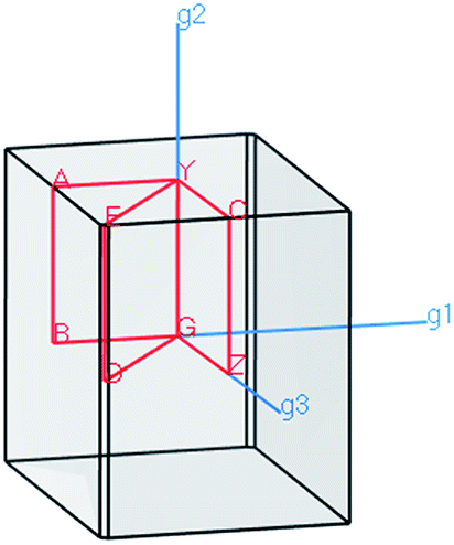 | ||
| Fig. 3 The reciprocal lattice corresponding to the unit cell of PE-Sn2P2S6 and FE-Sn2P2S6 structure with the coordinates of the special points in the BZ structure. | ||
In Fig. 4, the energy band spectra calculated using the three abovementioned functionals are presented. It can be observed that for both structures, the shapes of the conduction band minimum (CBM) and the valence band maximum (VBM) are similar as compared to the results obtained from the application of different functionals. The energy level indicating the VBM and CBM were observed to be shifted to a lower and higher energy value, respectively, comparing the obtained data from the LDA and GGA/PBE versus that obtained from the HSE06 functional. The energy gap calculated by applying all the used functionals presents an indirect character. The VBM and CBM are located at the same points of the BZ for both the PE and FE structures, and it does not depend on the functional character. The used functionals have only an influence on the change in the energy gap value of the calculated structure, moving the energy band levels but not changing the dispersion curves.
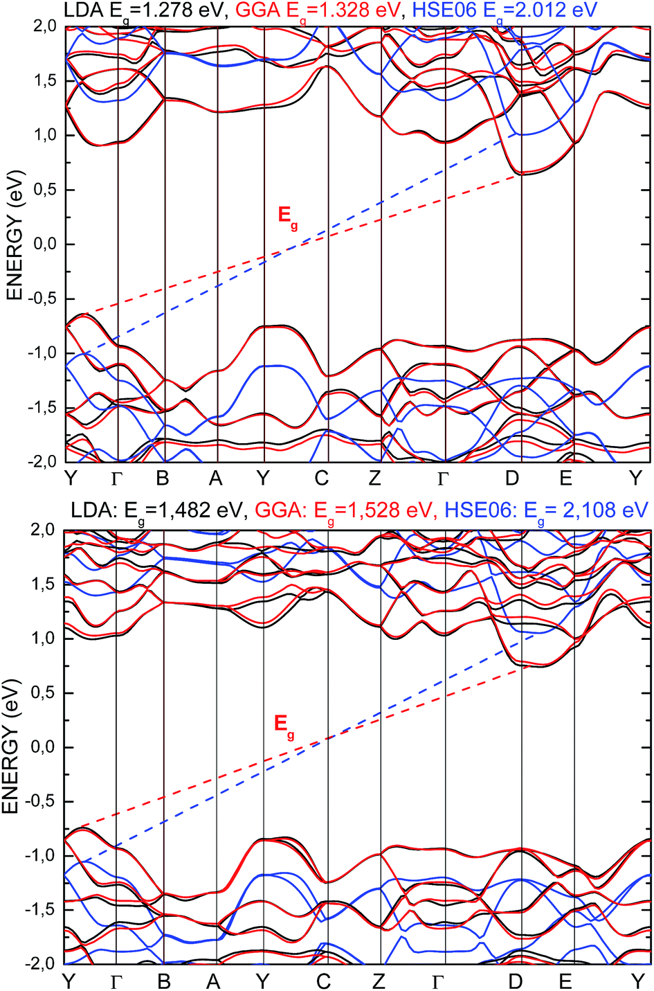 | ||
| Fig. 4 Energy band structure calculated for the PE-Sn2P2S6 (top) and FE-Sn2P2S6 (bottom) single crystals using LDA (black), GGA/PBE (red), and HSE06 (blue) functionals. | ||
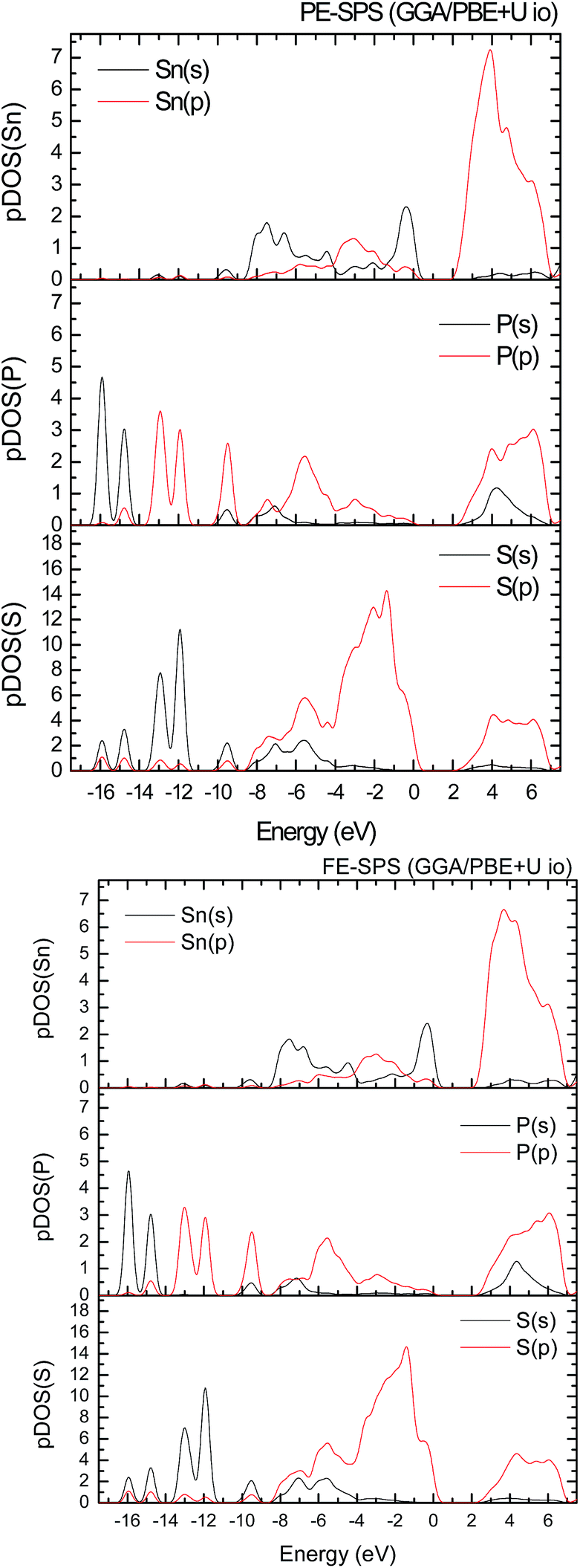
To improve the results of the performed calculations, the Hubbard model was proposed. The Hubbard parameters U were evaluated for different combinations of all atoms creating the SPS crystal. First, the U value was simultaneously changed from 0 up to 4 eV for the p-orbitals of tin, sulfur, and phosphorus atoms. The Hubbard parameters were applied only for the p orbitals because the energy states in the vicinity of the energy gap were mainly formed by the p-orbitals of all the presented atomic types. It can be seen that the partial density of states calculated for the PE and FE phase of the SPS crystal (see Fig. 5) are consistent with the results presented in the study of Glukhov.37 The Hubbard correction applied for the s-orbitals does not have any influence on the SPS band gap modification. The influence of the chosen Hubbard parameters U on the calculated band gap of both phases of the SPS single crystals is summarized in Table 4. It can be observed that within the DFT/PBE+U approach, the band gap increases with the increasing value of U applied for all atoms. It confirms the fact that the Hubbard-like correction term, taken into account via the GGA/PBE+U methodology, effectively improves the accuracy of the calculated band gap as compared to that considered via the conventional GGA/PBE method. The value of the computed band gap is in good agreement with the experimental values when the U parameter is equal to 4 eV for Sn, S, and the P atoms (last column in Table 4).
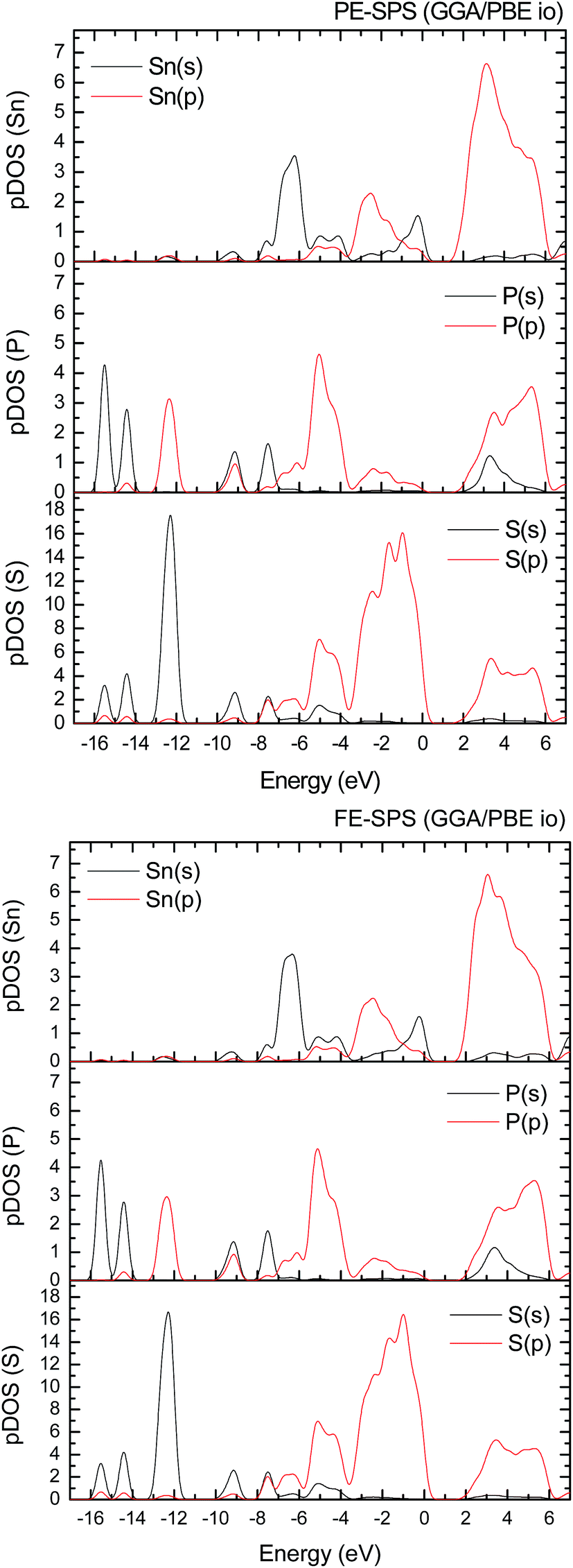 | ||
| Fig. 5 Partial densities of state (pDOS) calculated using a combination of the structural relaxation of ionic positions and the GGA/PBE approach for the PE-SPS (top panel) and for FE-SPS crystal (bottom panel). | ||
Aiming to elucidate that which atomic orbitals have the largest impact on the calculated band gap of the SPS crystal, the Hubbard parameters equal to 4 eV for the p-orbitals of different atoms were applied. The obtained results are shown in Table 5. It can be observed that the best results are obtained when U = 4 eV is used for the p-orbitals of the S and P atoms at the same time (bold data in Table 5). It means that the electron–electron correlations are the most significant between the S and P atoms. This is caused by the very short distance between the S and P atoms in the PE-SPS crystal (see Table 3), and as a consequence, their electron cloud overlapping is most important. Moreover, this is in agreement with the fact that the (P2S6)−4 anion complexes are the most tightly bonded formations in the investigated structure. Analyzing the data shown in Table 3, it can be seen that via applying the GGA/PBE approach, the optimized interatomic distances demonstrate a serious discrepancy between the calculated and experimental values, particularly for the Sn–S bond lengths. The abovementioned discrepancy reaches even 12% for the PE-SPS structure. The discussed difference comes down to acceptable 4% when the GGA/PBE+U methodology is applied. Because the best results of the energy gap value were obtained by taking into account U = 4 eV for the p-orbitals of the S and P atoms and also the structural parameters using GGA/PBE+U were optimized to be acceptable, further consideration were made only with these parameters. The band structures and the partial density of states calculated for the PE and FE phase of the Sn2P2S6 single crystals using the GGA/PBE+U functional with the U parameter equal to 4 eV for the S and P atoms and U = 0 eV for the Sn atom are presented in Fig. 6 and 7, respectively. These data were compared to the results obtained via the standard GGA/PBE functional. The most interesting changes in the energy bands topology were observed in two energy regions (Fig. 6). First is the region in the vicinity of the energy gap where lifting of the conduction bands is observed. The second energy region significantly influenced by the Hubbard correction includes two groups of energy bands located in the ranges from −14 eV up to −11 eV and from −11 eV up to −8 eV. Additionally, Hubbard terms push up the abovementioned bands but not equidistantly. The distances between these dispersion curves increases. On comparing the pDOS (Fig. 7) calculated using the Hubbard correction with that performed by the pure GGA/PBE methodology (Fig. 5) over the energy range (−14÷–11) eV, the splitting of the single peak was observed. These energy states correspond to the bonding and antibonding states formed by the hybridized sulfur s- and phosphorous p-orbitals. An increase in the energy distance between these states corresponds to an increase in the ionicity of the chemical bonding in both phases of the SPS crystals. On comparing Fig. 5 and 7, it can be concluded that taking into account the Hubbard correction, the contribution of the p-orbitals decreases with a simultaneous increase and lifting of the s-orbitals in the middle and topmost parts of the valence band (−10÷0) eV. Moreover, interesting modifications of the pDOS shape calculated for the tin atom was observed. However, in the studied crystals, the electron lone pair of the Sn cations in the 5s2 configuration is stereoactive, whereas the s orbitals of the cations are hybridized with the p orbitals of the S atom. When the U parameter for the p orbitals of the S atoms was used, the s-electrons attributed to the lone pair (−8÷–6) eV significantly changed their energy distribution and mainly mixed with the p-orbitals of the sulfur atoms on the top of the valence band. In this case, electron transfer from the antibonding energy level on the cation orbitals was observed. This is in agreement with the work of Vysochanskii et al.18 where the important role of the Sn 5s electron hybridization with the S 3p atomic orbitals in the VBM creation and their antibonding Sn 5s–S 3p orbitals mixing with P 3p orbitals was presented. The VBM of the FE-SPS is also formed by the p orbitals of S and s orbitals of the Sn atoms. As it was presented for PE-SPS, the CBM is constructed by the p orbitals of the Sn atoms with a small hybridization of the p orbitals of the S and P atoms. The used Hubbard parameters do not have a significant influence on the shape of pDOS for both the PE and FE-SPS structures as compared to the results obtained by the GGA/PBE methodology. The obtained results are in agreement with the data presented by Piacentini et al.58 and show that in some transition metal thiophosphates, the valence band mainly consists of levels belonging to the (P2S6)4− anions. This was also observed for the M2P2S6 (M = Fe, Ni, and Zn) crystals.59,60
| U | Snp | Sp | Pp | (S, Sn)p | (P, Sn)p | (S, P)p | (S, P, Sn)p |
|---|---|---|---|---|---|---|---|
| PE – Eg [eV] | 1.56 | 2.21 | 1.70 | 2.15 | 1.62 | 2.27 | 2.207 |
| FE – Eg [eV] | 1.76 | 2.34 | 1.85 | 2.29 | 1.80 | 2.38 | 2.337 |
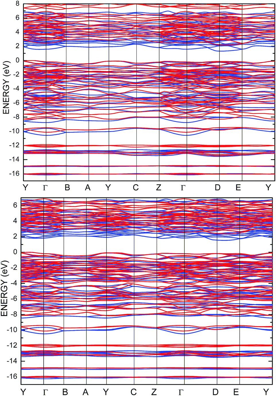 | ||
| Fig. 6 Energy band structure calculated for the PE-SPS (top panel) and FE-SPS (bottom panel) single crystals using the GGA/PBE (blue) and the GGA/PBE+U (red) functionals. | ||
 | ||
| Fig. 7 Influence of the Hubbard parameter U = 4 eV applied for the p electrons of S and P atoms on the partial density of state (pDOS) calculated for the PE-SPS (top panel) and FE-SPS (bottom panel) crystals. | ||
Analyzing the results of the performed investigations, it can be suggested that the most significant influence of the U parameters on the energy gap is observed by applying the correction for the S and P atoms. The application of the Hubbard correction for the Sn atom does not provide any important changes in the electronic properties of both the PE and FE phase of the SPS crystal. However, the role of the S atom is very important. This can be explained by the fact that the S atoms are characterized by the large number of localized charges as compared to the other atomic components. Note that the SPS crystal possesses an ionic-covalent bond character.18 The bonds between both the unequal Sn2+ ions and the (P2S6)4− clusters are ionic. Inside the (P2S6)4− cluster, evidence of strong covalent bonds between the phosphorus and sulfur atoms was observed. The SPS crystals contain three nonequivalent sulfur atoms, together with the phosphorus atom, creating a (PS3) structural pyramid. Moreover, note that the increasing values of U applied to the p-orbitals of the Sn, P, and S atoms increase the splitting between the energy states at the top of the valence band. Overall, the SPS crystals are constructed by the Sn2+ cations and (P2S6)4− anion clusters mostly joined by the ionic Sn–S bonds accompanied by the P–S and P–P covalent bonds. Neaton et al.61 also show that the increase in the Hubbard parameters shifts down by the energy of the top of the valence band. In the case of the SPS crystals, an effective coulomb repulsion parameter pushes the S p-bands down. The energy state, which mostly includes p orbitals of the P atoms, splits off from the state generally formed by the p orbitals of the S atoms (Fig. 7).
Mulliken population
To obtain an adequate picture of the chemical bonds and to explain the charge transfer features in the SPS crystals, the Mulliken populations were calculated for both phases. The calculated dependencies of the Mulliken charges versus the value of U are presented in Fig. 8. Mulliken population analysis can be used to characterize the electronic charge distribution in the studied system and to explore the bonding, antibonding or nonbonding nature of the molecular orbitals for particular atom pairs. The Hubbard parameter describes the energy of the coulomb repulsion of the electron pair with opposite spins, localized at the same site. At first glance, it may be expected that addition of the coulomb repulsion to the S and P orbitals will push out additional charges from the (P2S6)4− anion complexes towards Sn ions, such that causing lowering of the total ionicity of the considered crystal. The performed calculations show that U correction in combination with a relaxation of the ionic position has an opposite effect on the Mulliken charge changes. The absolute values of the charges donated by tin ions and accepted by sulfur ions increases with the increasing U parameters (see Fig. 8). Increasing the charge transfer makes the chemical bonds between the cations and the anion complexes more ionic. This was also demonstrated by the increase in the energy gap.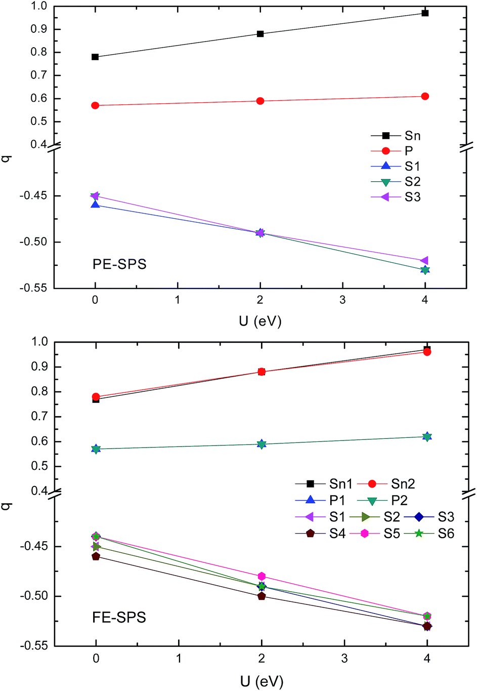 | ||
| Fig. 8 Influence of the Hubbard parameters on the Mulliken charge evaluation calculated for the PE-SPS (top panel) and FE-SPS crystals (bottom panel). | ||
The performed computer simulations show that the Mulliken charge transfer from the P and Sn atoms to the S atoms occurs for both SPS phases. However, the abovementioned transfer is more significant from the Sn atom to the S than that from the P atoms to S. This can be explained by the fact that the P and S atoms are accompanied by strong covalent bonds and important charge transfer from Sn cations to (PS3) anion complexes. As abovementioned, the p-orbitals of tin atoms form the bottom of the CB. A decrease in the charge on the p orbitals of tin atoms causes a shift-up of the CB energy. The charge transition from the Sn and P to the S atoms can be confirmed by the results reported by Kuepper et al.,12 where an interpretation of the electronic structure of Sn2P2S6 using X-ray photoelectron measurements was carried out. Sulfur and phosphorus were considered as the (P2S6)4− clusters with strong internal covalent bonds between the P and S atoms. Sulfur has a higher electron affinity compared to phosphorus; therefore, it is negatively charged. It has been confirmed that the chemical shift in the S 2p X-ray photoemission spectrum lowers the binding energies. It was shown that sp hybridization between P and S dominates the center of the valence band, where some influence of the Sn 5s states is also present. This influence explains the charge transition between the orbitals of the (PS3) clusters and orbitals of the Sn atoms. The difference between the electronegativity of sulfur (2.44) and phosphorus (2.06) leads to significant electron charge transfer from phosphorus to sulfur. Thus, the P–S chemical bonds also show ionic character in all the investigated sulfides.
Conclusions
The present study confirms that the electronic properties of chalcogenides can be calculated using DFT methodology augmented by Hubbard correction. Underlining the performed investigations, it can be suggested that the most significant influence of the U parameters on the energy gap of the SPS crystal is observed by applying a correction for the S and P atoms. The application of the Hubbard correction for the Sn atom does not provide any important changes in the electronic properties of both the FE and PE-SPS crystals. Contrary to Sn, the role of S atom is very important. This can be explained by the fact that S atoms are characterized by a large number of localized charges as compared to the Sn and P atoms.It was also shown that the Hubbard parameters affect the Mulliken charges localized on the atoms. The presented results show that when the U parameter for the S atoms of the PE-SPS crystal is used, an increase in the charge transfer from Sn and P atoms to the S atoms is observed. As a consequence, the charge localization on the S atom increases. An increase of the U parameters in the case of the FE-SPS crystal causes the Mulliken charge transfer from the Sn atoms to S atoms, as it is observed for the PE-SPS structure. The U parameters almost do not have any influence on the Mulliken charge evaluation of phosphorus atoms. For both phases of the SPS crystal, the transfer of charge is more significant from Sn atom to S than that from P atom to S. This can be explained by the fact that the P and S atoms are accompanied by strong covalent bonds, and additionally, the important charge transfer from Sn cation to (PS3) anion complex occurs.
For analyzing the charge redistribution in both SPS phases, the Hubbard correction was applied and it was shown that taking into account the additional coulomb interaction, the ordering of the bond length become consistent with the values of the interatomic orbital overlapping. Together with the adequate values of the band gap obtained by the DFT/PBE+U method, the abovementioned results allow us to conclude that the correlated electronic states play an important role in the considered systems. To the best of our knowledge, in the present study, the optimal values of the Hubbard parameters for the SPS crystal atoms were obtained for the first time. In future, these data can be used to investigate the optical properties of the SPS crystals or other chalcogenides. They may also be used to construct an effective Hubbard-like Hamiltonian for the description of the electron–electron and electron–phonon interactions as well as for the analysis of the possible excitonic condensation arising in ferroelectric semiconductor complexes. The predicted Hubbard parameters and the methodology implemented in the present study are helpful in explaining the metal-insulator phase transition taking place in the SPS crystal at high pressures.13,62
Acknowledgements
The calculations were performed at the Wroclaw Center for Networking and Supercomputing <http://www.wcss.wroc.pl> (Grant No. 171). The MATERIALS STUDIO package was used under the POLAND COUNTRY-WIDE LICENSE. The work was created as a result of the research project No. 2016/21/N/ST3/00461 funded by the National Science Centre.Notes and references
- J. W. Bennett and K. M. Rabe, J. Solid State Chem., 2012, 195, 21–31 CrossRef CAS.
- A. A. Grabar, Y. M. Vysochanskii, A. N. Shumelyuk, M. Jazbinsek, G. Montemezzani and P. Gunter, Photorefractive effect in the red and near infrared regions of spectrum, Chapter in a book, Photorefractive Materials and Their Applications, ed. P. Gunter and J. Huignard, Springer Verlag, Heidelberg, 2006 Search PubMed.
- P. Mathey, G. Gadret, A. Grabar, I. Stoika and Y. Yysochanskii, Opt. Commun., 2013, 300, 90 CrossRef CAS.
- R. Mosimann, P. Marty, T. Bach, F. Juvalta, M. Jazbinsek, P. Gunter and A. A. Grabar, Opt. Lett., 2007, 32, 3230 CrossRef CAS PubMed.
- R. Mosimann, D. Haertle, M. Jazbinsek, G. Montemezzi and P. Gunter, J. Opt. Soc. Am. B, 2006, 23, 1620 CrossRef CAS.
- Y. W. Cho, S. Choi and Y. M. Vysochanskii, J. Mater. Res., 2001, 16, 3317 CrossRef CAS.
- D. Haertle, G. Caimi, A. Haldi, G. Montemezzani, P. Gunter, A. A. Grabar, I. M. Stoika and Y. M. Vysochanskii, Opt. Commun., 2003, 215, 333 CrossRef CAS.
- M. M. Maior, M. I. Gurzan, S. B. Molnar, I. P. Prits and Y. M. Vysochanskii, IEEE Trans. Sonics Ultrason., 2000, 47, 877 CrossRef CAS PubMed.
- D. A. Cleary, R. D. Willet, F. Ghebremichael and M. G. Zuzyk, Solid State Commun., 1993, 88, 39 CrossRef CAS.
- J. Grigas, E. Talik, V. Lazauskas, Y. M. Vysochanskii, R. Yevych, M. Adamiec and V. Nelkinas, Ferroelectrics, 2009, 378, 70 CrossRef CAS.
- Y. Rong, M. Li, J. Chen, M. Zhou, K. Lin, L. Hu, W. Yuan, W. Duan, J. Dengc and X. Xing, Phys. Chem. Chem. Phys., 2016, 18, 6247 RSC.
- K. Kuepper, B. Schneider, V. Caciuc, M. Neumann, A. V. Postnikov, A. Ruediger, A. A. Grabar and Y. M. Vysochanskii, Phys. Rev. B: Condens. Matter Mater. Phys., 2003, 67, 115101 CrossRef.
- S. V. Ovsyannikov, H. Gou, N. V. Morozova, I. Tyagur, Y. Tyagur and V. V. Shchennikov, J. Appl. Phys., 2013, 113, 013511 CrossRef.
- T. Bach, M. Jazbinsek, G. Montemezzani, P. Günter, A. A. Grabar and Y. M. Vysochanskii, J. Opt. Soc. Am. B, 2007, 24, 1535 CrossRef CAS.
- I. V. Kedyk, P. Mathey, G. Gadret, A. A. Grabar, K. V. Fedyo, I. M. Stoika, I. P. Prits and Y. M. Vysochanskii, Appl. Phys. B, 2008, 92, 549 CrossRef CAS.
- A. Shumelyuk, D. Barilov, M. Imlau, A. Grabar, I. Stoyka and Y. Vysochanskii, Opt. Mater., 2008, 30, 1555 CrossRef CAS.
- K. Z. Rushchanskii, A. Molnar, R. Bilanych, R. Yevych, A. Kohutych, Y. M. Vysochanskii, V. Samulionis and J. Banys, Phys. Rev. B, 2016, 93, 014101 CrossRef.
- Y. M. Vysochanskii, D. Baltrunas, A. A. Grabar, K. Mazeika, K. Fedyo and A. Sudavicius, Phys. Status Solidi B, 2009, 246, 1110 CrossRef CAS.
- O. Mys, B. Zapeka, I. Martynyuk-Lototska and R. Vlokh, Opt. Mater., 2012, 35, 168 CrossRef CAS.
- A. Reudiger, O. Schirmer, S. Odoulov, A. Shumelyuk and A. Grabar, Opt. Mater., 2001, 18, 123 CrossRef.
- A. A. Bogomolov, A. V. Solnyshkin, D. A. Kiselev, I. P. Raevsky, N. P. Protzenko and D. N. Sandjiev, J. Eur. Ceram. Soc., 2007, 27, 3835 CrossRef CAS.
- M. Jazbinšek, D. Haertle, G. Montemezzani and P. Günter, J. Opt. Soc. Am. B, 2005, 22, 2459 CrossRef.
- E. I. Gerzanieh, P. P. Guranich, A. G. Slivka, V. S. Shusta, M. I. Gurzan and V. M. Kedyulieh, Russ. Phys. J., 1997, 40, 784 CrossRef.
- A. Shumelyuk, M. Wesner, M. Imlau and S. Odoulov, Appl. Phys. B, 2009, 95, 497 CrossRef CAS.
- K. Z. Rushchanskii, Y. M. Vysochanskii and D. Strauch, Phys. Rev. Lett., 2007, 99, 207601 CrossRef PubMed.
- Y. Vysochanskii, K. Glukhov, K. Fedyo and R. Yevych, Ferroelectrics, 2011, 414, 30 CrossRef CAS.
- A. A. Lavrentyev, B. V. Gabrelian, I. Y. Nikifororv, J. J. Rehr and A. L. Ankudinov, J. Phys. Chem. Solids, 2003, 64, 2479 CrossRef CAS.
- K. Z. Rushchanskii, Y. M. Vysochanskii, V. B. Cajipe and X. Bourdon, Phys. Rev. B: Condens. Matter Mater. Phys., 2007, 73, 115115 CrossRef.
- J. Kuneš, J. Phys.: Condens. Matter, 2015, 27, 333201 CrossRef PubMed.
- A. I. Chobal, I. M. Rizak, A. G. Grebenyuk and V. M. Rizak, Phys. Solid State, 2010, 52, 1468 CrossRef CAS.
- G. Dittmar and H. Schafer, Z. Naturforsch., B: Anorg. Chem., Org. Chem., 1974, 29, 312 CAS.
- B. Scott, M. Pressprich, R. D. Willet and D. A. Cleary, J. Solid State Chem., 1992, 96, 294 CrossRef CAS.
- P. Hohenberg and W. Kohn, Phys. Rev. [Sect.] B, 1964, 136, B864 CrossRef.
- W. Kohn and L. J. Sham, Phys. Rev. A, 1965, 140, A1133 CrossRef.
- Y. Wang and J. P. Perdew, Phys. Rev. B: Condens. Matter Mater. Phys., 1991, 44, 13298 CrossRef.
- J. P. Perdew, K. Burke and M. Ernzerhof, Phys. Rev. Lett., 1996, 77, 3865 CrossRef CAS PubMed.
- K. Glukhov, K. Fedyo, J. Banys and Y. Vysochanskii, Int. J. Mol. Sci., 2012, 13, 14356 CrossRef CAS PubMed.
- V. Zolyomi, N. D. Drummond and V. I. Falko, Phys. Rev. B: Condens. Matter Mater. Phys., 2014, 89, 205416 CrossRef.
- L. Hedin, Phys. Rev. A, 1965, 139, 796 CrossRef CAS.
- H. Iikura, T. Tsuneda, T. Yanai and K. Hirao, J. Chem. Phys., 2001, 115, 3540 CrossRef CAS.
- H. Sekino, Y. Maeda and M. Kamiya, Mol. Phys., 2005, 103, 2183 CrossRef CAS.
- Y. Tawada, T. Tsuneda, S. Yanagisawa, T. Yanai and K. Hirao, J. Chem. Phys., 2004, 120, 8425 CrossRef CAS PubMed.
- M. Kamiya, H. Sekino, T. Tsuneda and K. Hirao, J. Chem. Phys., 2005, 122, 234111 CrossRef PubMed.
- M. Makowska-Janusik, O. Gladii, A. Kassiba, J. Boucle and N. Herlin-Boime, J. Phys. Chem. C, 2014, 118, 6009 CAS.
- M. A. Ruiz Preciado, A. Kassiba, A. Morales-Acevedo and M. Makowska-Janusik, RSC Adv., 2015, 5, 17396 RSC.
- V. I. Anisimov, J. Zaanen and O. K. Andersen, Phys. Rev. B: Condens. Matter Mater. Phys., 1991, 44, 943 CrossRef CAS.
- V. I. Anisimov, I. V. Solovyev, M. A. Korotin, M. T. Czyzyk and G. A. Sawatzky, Phys. Rev. B: Condens. Matter Mater. Phys., 1993, 48, 16929 CrossRef CAS.
- V. I. Anisimov, F. Aryasetiawan and A. I. Lichtenstein, J. Phys.: Condens. Matter, 1997, 9, 767 CrossRef CAS.
- S. Ishihara, T. Egami and M. Tachiki, Phys. Rev. B: Condens. Matter Mater. Phys., 1994, 49, 8944 CrossRef.
- S. J. Clark, M. D. Segall, C. J. Pickard, P. J. Hasnip, M. J. Probert, K. Refson and M. C. Payne, Z. Kristallogr., 2005, 220, 567 CAS.
- B. G. Pfrommer, M. Cate, S. G. Louie and M. L. Cohen, J. Comput. Phys., 1997, 131, 233 CrossRef CAS.
- J. Heyda and G. E. Scuseria, J. Chem. Phys., 2004, 121, 1187 CrossRef PubMed; A. V. Krukau, O. A. Vydrov, A. F. Izmaylov and G. E. Scuseria, J. Chem. Phys., 2006, 125, 224106 CrossRef PubMed.
- D. Vanderbilt, Phys. Rev. B: Condens. Matter Mater. Phys., 1990, 41, 7892 CrossRef.
- A. A. Bogomolov, O. V. Malyshkina, A. V. Solnyshkin, I. P. Raevsky, N. P. Protzenko and D. N. Sandjiev, Ferroelectrics, 1998, 214, 131 CrossRef CAS.
- A. A. Bogomolov, A. V. Solnyshkin, D. A. Kiselev, I. P. Raevskii, N. P. Protsenko and D. N. Sandzhiev, Phys. Solid State, 2006, 48, 1192 CrossRef CAS.
- R. Caracas and X. Gonze, Phys. Rev. B: Condens. Matter Mater. Phys., 2002, 66, 104106 CrossRef.
- I. P. Studenyak, V. V. Mitrovcij, G. S. Kovacs, O. A. Mykajlo, M. I. Gurzan and Y. M. Vysochanskii, Ferroelectrics, 2001, 254, 295–310 CrossRef CAS.
- M. Piacentini, F. S. Khumalo, C. G. Olson, J. Anderegg and D. W. Lynch, Chem. Phys., 1982, 65, 289 CrossRef CAS.
- M. Piacentini, F. S. Khumalo, G. Leveque, C. G. Olson and D. W. Lynch, Chem. Phys., 1982, 72, 61 CrossRef CAS.
- G. M. Curro, V. Grasso, F. Neri and L. Silipigni, Il Nuovo Cimento D, 1998, 20, 1163 CrossRef.
- J. B. Neaton, C. Ederer, U. V. Waghmare, N. A. Spaldin and K. M. Rabe, Phys. Rev. B: Condens. Matter Mater. Phys., 2005, 71, 014113 CrossRef.
- S. V. Ovsyannikov, H. Gou, N. V. Morozova, I. Tyagur, Y. Tyagur and V. V. Shchennikov, J. Appl. Phys., 2013, 113, 013511 CrossRef.
| This journal is © The Royal Society of Chemistry 2017 |