
 Open Access Article
 This Open Access Article is licensed under a Creative Commons Attribution-Non Commercial 3.0 Unported Licence
Tuning the Schottky contacts at the graphene/WS2 interface by electric field
Fang Zhang a,
Wei Libc,
Yaqiang Mac,
Yanan Tangd and
Xianqi Dai*cd
a,
Wei Libc,
Yaqiang Mac,
Yanan Tangd and
Xianqi Dai*cd
aCollege of Electric and Mechanical Engineering, Pingdingshan University, Pingdingshan 467000, China
bSchool of Mathematics & Physics, Henan University of Urban Construction, Pingdingshan 467036, China
cCollege of Physics and Materials Science, Henan Normal University, Xinxiang 453007, China. E-mail: xqdai@htu.cn
dDepartment of Physics, Zhengzhou Normal University, Zhengzhou, Henan 450044, China
First published on 6th June 2017
Abstract
Using the first-principle calculations, we study the electronic structures of graphene/WS2 van der Waals (vdW) heterostructures by applying an external electric field (Eext) perpendicular to the heterobilayers. It is demonstrated that the intrinsic electronic properties of graphene and WS2 are quite well preserved due to the weak vdW contact. We find that n-type Schottky contacts with a significantly small Schottky barrier are formed at the graphene/WS2 interface and p-type (hole) doping in graphene occurs during the formation of graphene/WS2 heterostructures. Moreover, the Eext is effective to tune the Schottky contacts, which can transform the n-type into p-type and ohmic contact. Meanwhile, p-type (hole) doping in graphene is enhanced under negative Eext and a large positive Eext is required to achieve n-type (electron) doping in graphene. The Eext can control not only the amount of charge transfer but also the direction of charge transfer at the graphene/WS2 interface. The present study would open a new avenue for application of ultrathin graphene/WS2 heterostructures in future nano- and optoelectronics.
1. Introduction
Two-dimensional (2D) ultrathin materials have received considerable attention recently owing to their outstanding mechanical, thermal, optical, electronic and chemical properties, which make these materials promising for next-generation nanoelectronic and optoelectronic devices.1–7 Graphene, a 2D sp2-hybridized 1carbon monolayer has been reported as one of the most fascinating 2D materials8–11 because of its extraordinary properties including massless Dirac fermions, high carrier mobility and intriguing quantum Hall effect.12,13 However, the absence of a bandgap restrains its wide application in electronic devices, particularly for logic circuits.14,15 Subsequently to the graphene isolation, a whole new class of 2D materials has been investigated, such as the transition metal dichalchogenides (TMDs). However, in contrast to the gapless graphene, the semiconducting TMDs possess a finite bandgap.16 Tungsten disulfide (WS2), one of the members in the TMDs family, has been recently studied for various electronic devices applications.17,18 WS2 belongs to the P63/mmc space group (a = 3.155, c = 12.36), and has a vdW layered structure where each layer consists of a slab S–W–S sandwich.19 Bulk WS2 is an indirect gap semiconductor, it has a bandgap of 1.3 eV.20 However, studies demonstrate that with decreasing number of layers, WS2 transforms from indirect gap (in bulk) into direct gap (in monolayer).21 Moreover, the monolayer WS2 possess a sufficiently high in-plane carrier mobility and a high on/off current ratio, which can be applied in photodetectors, field-effect transistors, and electronic devices.22,23Currently, vertical heterostructures based on 2D vdW materials, especially heterobilayers made layer by layer from 2D monolayers, are being considered as a promising method to construct devices that integrate the properties of their respective components24–26 with ideal properties to be applied in nanoelectronics and optoelectronics. Many 2D vertical ultrathin vdW heterostructures, have been widely studied experimentally and theoretically, such as graphene/MoS2,27–30 graphene/h-BN,31–33 BN/TMD,34,35 phosphorene/TMD,36 TMD/TMD37–39 and phosphorene/graphene.40,41 These vdW heterostructures show many new optoelectronic properties far beyond individual components. Moreover, due to the lack of dangling bonds and the weak electron coupling at the interface of vdW heterobilayers, their intrinsic electronic properties are well preserved without any degradation. Among these vdW heterobilayers, graphene-based vdW heterostructures have attracted considerable interest. Hu et al.42 reported that interlayer interactions in graphene/silicene heterostructure induce tunable p-type and n-type doping of silicene and graphene, respectively, indicating their doping carrier concentrations can be tuned by their interfacial spacing. Graphene on h-BN substrates have mobilities and carrier inhomogeneities that are almost an order of magnitude better than devices on SiO2, which show reduced roughness, intrinsic doping and chemical reactivity.36 Tan et al.43 showed that photoirradiation of the WS2 on graphene region caused further Dirac point shifts, indicative of a reduction in the p-type doping levels of graphene, revealing that the photogenerated excitons in WS2 are split across the heterostructure by electron transfer from WS2 to graphene.
Recently, a new generation of field-effect transistors where 2D WS2 serves as an atomically thin barrier between two layers of mechanically exfoliated graphene have been constructed successfully.44 In comparision with MoS2, WS2 allows for switching between tunneling and thermionic transport regimes, resulting in much better transistor characteristics and thus allowing for much higher ON/OFF ratios and much larger ON current. The performance of vertical field-effect transistor based on graphene–WS2 heterostructures depends on the tunability of the Schottky barrier via a shift in the Fermi level of the graphene and changes in the height and type of the barrier. Our recent work45 have demonstrated that the Eext can not only control the Schottky barrier height but also the Schottky contacts (n-type and p-type) and ohmic contacts (n-type) at the interface of arsenene/graphene vdW heterostructures. Therefore, an interesting question arise: whether Eext for Schottky barrier tuning can also be employed in graphene/WS2 vdW heterostructure? Therefore, in the present work, we investigate the electronic properties of graphene/WS2 vdW heterostructure by first-principles calculations, but the main points are the electrically tunable Schottky barriers of graphene/WS2 heterobilayer.
2. Computational methods and models
We use density functional theory (DFT) calculations implemented in the Vienna Ab-Initio Simulation Package (VASP).46 The generalized gradient approximation (GGA) by the Perdew–Burke–Ernzerhof (PBE) functional is utilized as the exchange–correlation functional.47 The non-bonding vdW interaction is incorporated by adding a semi-empirical dispersion potential to the conventional Kohn–Sham DFT energy, through a pair-wise force field following Grimme's DFT-D3 method.48 The projected augmented wave (PAW) potential49 is employed to describe the electron-ion potential. We set the energy cutoff as 500 eV. A 9 × 9 × 1 Monkhorst–Pack mesh was used for relaxation calculations and a 15 × 15 × 1 Monkhorst–Pack mesh was used post-relaxation for static electronic structure calculations. All atoms are allowed to be fully relaxed until the atomic Hellmann–Feynman forces are smaller than 0.01 eV Å−1 and the convergence criterion of energy in the self-consistency process is set to 10−5 eV. A vacuum space of 20 Å in the z direction is used to avoid the interactions between neighboring slabs. The Eext is introduced in the VASP by the dipole layer method with the dipole placed in the vacuum region of the periodic supercell.50 In addition, the spin-orbital coupling (SOC) effects are included in the self-consistent calculations of electronic structures to verify its effects in the heterostructures.The calculated lattice parameters of the pristine monolayer WS2 and graphene are 3.18 Å and 2.46 Å, respectively. We choose WS2 as a substrate to match with graphene. The supercell of our system is composed of 4 × 4 primitive graphene cells (32 carbon atoms) and 3 × 3 WS2 primitive cells (18 sulfur and 9 tungsten atoms) along the x and y directions. The lattice mismatch is 3.1% for the composed configuration. The equilibrium geometry of the system is shown in Fig. 1(a) and (b).
 | ||
| Fig. 1 Top view (a) and side view (b) of the graphene/WS2 vdW heterostructure. The gray, blue and yellow balls are for carbon, tungsten and sulfur atoms, respectively. A vertical Eext is applied perpendicular to the layers. The interlayer distance D between graphene and WS2 is marked. | ||
3. Results and discussion
In order to get the equilibrium position of the monolayer WS2 with respect to the graphene layer, we calculated the binding energy between the monolayer WS2 and graphene. After fixing the WS2 layer, we move the WS2 layer with respect to the graphene layer to make sure this is really the minimum binding energy. The binding energy (Eb) per carbon atom between the graphene sheet and the monolayer WS2 is calculated as Eb = [Egraphene/WS2 − (Egraphene + EWS2)]/N, where Egraphene/WS2 is the total energy of the graphene/WS2 vdW heterostructure, Egraphene is the total energy of the isolated graphene layer, EWS2 is the total energy of the isolated WS2 monolayer, and N = 32 is the number of carbon atoms in the supercell. For the graphene/WS2 heterobilayer, the calculated binding energy per carbon atom is −26.8 meV with an equilibrium interlayer distance of 3.49 Å. The negligible binding energy and the large interlayer distance (much larger than the sum of the covalent radii of the carbon and sulfur atoms) indicate that weak vdW interactions dominate in the graphene/WS2 heterobilayer, similar to other 2D vdW graphene-based heterostructures.51,52To further explore the bonding of graphene and WS2 monolayer, we studied the charge density difference of the graphene/WS2 heterostructure, as indicated in Fig. 2. The charge density difference is defined as:
| Δρ = ρgraphene/WS2(r) − ρgraphene(r) − ρWS2(r) |
 | ||
| Fig. 2 Top view (a) and side view (b) of differential charge density of the graphene/WS2 heterostructure. The gray, blue and yellow balls are for carbon, tungsten and sulfur atoms, respectively. Orange and green isosurfaces correspond to the accumulation and depletion of electronic densities (the isovalue is 4.1 an10−5 e Å−3). | ||
In heterostructures based on vertical stacking of monolayer materials, strain will be present due to lattice mismatches. In the graphene/WS2 heterostructure there is a 3.1% lattice mismatch, so there is artificial tensile strain on WS2 and compressive strain on graphene. To correct the artificial strain effect, we investigate uniaxial absolute deformation potentials, which relate the strain to the shifts of individual band edges. The uniaxial absolute deformation potentials can be defined as  ,
, 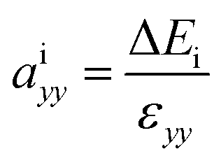 , where ai is the deformation potential of a given state, ΔEi is the shift of its energy under strain, and εxx, εyy are the normal strains in x and y directions. In our electronic structure calculations, we use the vacuum level to align the energies of the electronic states. The calculated absolute deformation potentials of the CBM and VBM of WS2 and the Dirac point of graphene are presented in Table 1. The absolute deformation potentials allow one to directly obtain the energy shifts of the individual band edges upon application of strain to achieve correcting the artificial strain effect.
| aVBMΓ | aCBMΓ | aDiracK | |
|---|---|---|---|
| xx | 1.56 | 6.79 | 0.023 |
| yy | 1.68 | 6.91 | 0.021 |
To understand the electronic properties of graphene/WS2 heterostructure, the electronic structures of pristine graphene and monolayer WS2 are checked and their energy band structures are plotted in Fig. 3(b) and (c), respectively. It shows that graphene has a zero bandgap and retains its metallic character, which is consistent with previous theoretical studies.53,54 Considering the SOC effects, Fig. 3(c) presents that the pristine WS2 monolayer is a direct semiconductor at the Γ point with a bandgap of 0.91 eV, and the valence band splits by 115 meV, while the conduction band is not obviously split. Compared with the band structures of monolayer WS2 primitive cell, the conduction band minimum (CBM) and the valence band maximum (VBM) of the 3 VB3 monolayer WS2 supercell are mapped to the Γ point. The reason is that the inequivalent K and K′ points are folded and coupled into the same Γ-point when a 3 × 3 monolayer WS2 supercell is studied. Then, we investigate the electronic structure of the graphene/WS2 vdW heterostructure. The calculated band structure of the graphene/WS2 heterostructure including the SOC effect at the equilibrium interlayer distance is shown in Fig. 3(a). Red and blue denote the contributions from graphene and WS2 layer, respectively. Compared with the electronic band structures of the pristine graphene and monolayer WS2 shown in Fig. 3(b) and (c), respectively, the band structure of the graphene/WS2 heterostructure seems to be a simple sum of each component. The overall shape of band structure of graphene/WS2 heterostructure is basically in accord with the sum of the pristine graphene and monolayer WS2. Furthermore, it indicates that a vacuum space of 20 Å in the z direction is sufficient to avoid the interactions between neighboring sheets. The band contributed by graphene illustrates that the graphene layer remains its metallic character, and the band contributed by WS2 illustrates that the WS2 layer retains the direct bandgap at the Γ point with a bandgap of 0.91 eV. Thus, the main dominant sorts of binding forces of graphene/WS2 heterostructure are vdW interaction. The graphene/WS2 heterostructure can preserve the intrinsic excellent electronic properties of the individual materials. Fig. 3(b) shows that the Dirac point of the isolated graphene is at the Fermi level, however, the Fermi level of graphene/WS2 heterostructure moves down to below the Dirac point of graphene layer, which results in p-type (hole) doping in graphene. Because the electronic states around Fermi level at K point are all contributed from graphene layer (displayed in Fig. 3(a)), the move of Fermi level demonstrates that graphene layer lose electrons during the formation of graphene/WS2 heterostructure.
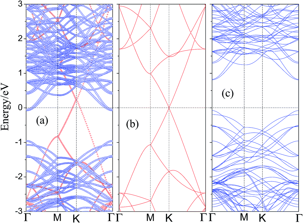 | ||
| Fig. 3 The projected band structure of (a) graphene/WS2 heterostructure, projection to graphene by red circles and WS2 layer is denoted by blue circles. Band structures of (b) pristine graphene and (c) pristine monolayer WS2. The Fermi level is set to zero and marked by black dashed lines. | ||
Interestingly, we found that a Schottky contact can be formed between metallic graphene and semiconducting WS2, the graphene/WS2 configuration is a representative metal–semiconductor heterostructure. From a device point of view, when using graphene as the metal contact and WS2 monolayer as the channel, the electrical current flow across the metal–semiconductor interface is usually non-linear against the applied bias voltage. For n-type semiconductors, electrons near the CBM carry the most of the current, and for p-type semiconductors, holes near the VBM are mainly responsible for electrical conduction. At the metal–semiconductor interface, the electrons near the CBM for n-type semiconductors can spontaneously flow to the metal. When electronic transport occurs across the metal–semiconductor interface, the states will be offset and the Fermi level is located above the midgap (CBM + VBM)/2, known as the n-type Schottky barrier and the n-type Schottky barrier (ΦBn) is defined as: ΦBn = EC − EF, where EC and EF are the CBM and the Fermi level, respectively. A rectifying behavior occurs between the n-type semiconductor and metal due to the n-type Schottky barrier. If the p-type semiconductor is in contact with the metal, the Fermi level is located below the midgap (CBM + VBM)/2, known as the p-type Schottky barrier and the p-type Schottky barrier (ΦBp) is defined as: ΦBp = EF − EV, where EF and EV are the Fermi level and the VBM, respectively. The current flow across the metal–semiconductor interface depends on the magnitude of the Schottky barrier height, so it is necessary to study the Schottky barrier of the graphene/WS2 interface. After analysis of the band structure of the graphene/WS2 heterostructure, shown in Fig. 3(a), we find that the ohmic contact is formed at the graphene/WS2 interface with the Fermi level through the conduction band of WS2 (ΦBn < 0).
For the performance of graphene/WS2 based field effect transistors, determination of the effect of Eext on the electronic properties of the graphene/WS2 heterobilayer is important. Therefore we study the effect of Eext on the interface electronic properties of graphene/WS2 heterostructure. The projected band structures of graphene/WS2 heterostructures under different Eext are shown in Fig. 4. In Fig. 4, with the negative Eext varies from 0 to −2 V nm−1, the CBM of WS2 below the Fermi level declines gradually, the ohmic contact is still preserved. Nevertheless, with the positive Eext varies from 0 to 1 V nm−1, the CBM of WS2 shifts upward and across the Fermi level, which indicates the n-type Schottky contact is formed. For graphene/WS2 heterostructure under an Eext of 1 V nm−1, the CBM of WS2 is closer to the Fermi level than the VBM of WS2, giving rise to the n-type Schottky barrier. As can be seen from Fig. 4, the Fermi level shifts from the CBM to the VBM of WS2 when the positive Eext increases from 1 V nm−1 to 2 V nm−1. The n-type Schottky barrier height exceeds p-type Schottky barrier height gradually, which demonstrates the positive Eext transforms the n-type Schottky contact into the p-type Schottky contact at the graphene/WS2 interface. When the positive Eext increases from 2 V nm−1 to 3 V nm−1, the valence band of WS2 moves upward and cross the Fermi level (ΦBp < 0), the ohmic contact is obtained again. What is more, as already pointed out, the Fermi level shifts down to below the Dirac point of graphene during the formation of graphene/WS2 heterostructure, leading to p-type (hole) doping in graphene as shown in Fig. 3. More electrons transfer from graphene's Dirac point to WS2's conduction band when the heterobilayer is subjected to a negative Eext, the shifts (ΔED) of graphene's Dirac point relative to the Fermi level in the graphene/WS2 heterostructure are 0.23, 0.58 and 0.96 eV under the Eext of 0 V nm−1, −1 V nm−1 and −2 V nm−1, respectively, p-type (hole) doping in graphene is enhanced under the negative Eext. On the contrary, the large positive Eext is needed to make the electrons overcome the bandgap (0.91 eV) of WS2 and then transfer electrons from WS2's valence band to graphene's Dirac point. Therefore, the shifts (ΔED) of graphene's Dirac point relative to the Fermi level retain almost zero under the positive Eext, n-type (electron) doping in graphene occurs until the positive Eext exceeds 2.4 V nm−1.
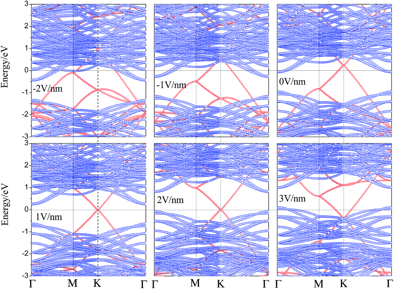 | ||
| Fig. 4 The projected band structures of graphene/WS2 heterostructures under different Eext, projection to graphene layer is denoted by red circles and to WS2 by blue circles. | ||
To quantitatively characterize the Schottky barrier height and Schottky doping of graphene/WS2 heterobilayer, the evolutions of ΦBp and ΦBn of graphene/WS2 heterostructure as a function of Eext are shown in Fig. 5. When the heterobilayer is subjected to the positive Eext, the electrons transfer from WS2 to graphene, the CBM of WS2 moves upward and across the Fermi level, which results in the form of n-type Schottky contact. With the further increase of the positive Eext, the valence (conduction) band of WS2 shifts toward (away from) the Fermi level, the magnitude of ΦBp gradually decreases and the magnitude of ΦBn gradually increases. As a result, the lines of ΦBp and ΦBn intersect at 1.35 V nm−1, where the n-type Schottky contact is changed to p-type Schottky contact. As the positive Eext increases more than 2.4 V nm−1, the valence band of WS2 will shift up and cross the Fermi level (ΦBp < 0), which demonstrates that ohmic contact is formed in the graphene/WS2 heterostructure. When the heterobilayer is subjected to the negative Eext, the electrons are transferred from graphene to WS2, the graphene/WS2 heterobilayer remains the ohmic contact. Therefore, the Eext is effective to tune the Schottky contacts, which can transform the n-type into p-type and ohmic contact.
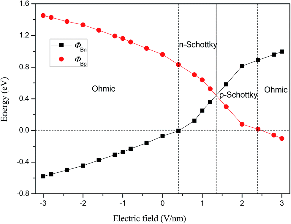 | ||
| Fig. 5 Evolution of Schottky barriers of ΦBp and ΦBn in graphene/WS2 heterostructurer as a function of Eext. | ||
Although the graphene layers and the WS2 layers binding together via vdW force, the distribution of interfacial charge will be altered in the graphene/WS2 heterostructure under different Eext, which may result in the Schottky barrier transition. To visualize the charge redistribution and further understand charge transfer mechanism between graphene and WS2 layer in the vdW heterobilayer, we plot the plane-averaged charge density difference Δρ(z) along the vertical direction to the heterobilayer, which can provide a quantitative picture of the charge redistribution at the interface. The plane-averaged charge density difference along the z direction is defined as:

 | ||
| Fig. 6 Plots of the plane-averaged charge density difference along z direction under various Eext. The red vertical dashed line denotes the intermediate position of the two monolayers. | ||
Finally, we would like to point out that conventional PBE methods underestimate the bandgap and Schottky barrier height of the heterostructures, but the HSE or quasi particle self-consistent GW methods are not still considered to correct it for all considered systems in this work due to their tremendously computational costs. We emphasize that our goal here is not to determine precise bandgaps and Schottky barrier heights but to illustrate the phenomenon of Schottky contacts tuning by external electric fields and to uncover the underlying physics. Moreover, PBE methods are good at predicting correct trends and physical mechanisms, which possesses guiding function for future experimental studies. Thus, for future related experimental studies, the numbers obtained in this work should be taken with care since it is likely that the obtained physical quantity should be underestimated.
4. Conclusions
In summary, the electronic properties of graphene/WS2 vdW heterostructures under different Eext are investigated by means of the first-principle calculations. We find that graphene interacts weakly with WS2 via weak vdW interactions and both the intrinsic electronic properties of graphene and WS2 are quite well preserved at the equilibrium interlayer distance. The n-type Schottky contacts with the significantly small Schottky barrier are formed in the graphene/WS2 heterostructure and p-type (hole) doping in graphene occurs during the formation of graphene/WS2 heterostructure. When the heterobilayer is subjected to the positive Eext, a transition from n-type to p-type Schottky contacts occurs at 1.35 V nm−1, then to ohmic contacts at 3 V nm−1. The graphene/WS2 heterostructure remains the n-type Schottky contact under the negative Eext less than −0.55 V nm−1. When the negative Eext exceeds −0.55 V nm−1, the ohmic contact is obtained again. p-Type (hole) doping in graphene is enhanced under the negative Eext and the large positive Eext is required to achieve n-type (electron) doping in graphene. The Eext can control not only the amount of charge transfer but also the direction of charge transfer at the graphene/WS2 interface. Our work is expected to promote the application of ultrathin graphene/WS2 heterostructure in the next-generation nanoelectronic and photonics devices.Acknowledgements
We acknowledge support from the National Natural Science Foundation of China (Grant No. 61674053, 11504092, U1404109 and 11504334) and the High Performance Computing Center of Henan Normal University.References
- J. Du, C. X. Xia, Y. M. Liu, X. P. Li, Y. T. Peng and S. Y. Wei, Appl. Surf. Sci., 2017, 401, 114–119 CrossRef CAS.
- J. Du, C. X. Xia, T. X. Wang, X. Zhao, X. M. Tan and S. Y. Wei, Appl. Surf. Sci., 2016, 378, 350–356 CrossRef CAS.
- H. Zhang, C. X. Xia, X. Zhao, T. X. Wang and J. B. Li, Appl. Surf. Sci., 2015, 356, 1200–1206 CrossRef CAS.
- X. Zhao, C. X. Xia, T. X. Wang, X. Q. Dai and L. Yang, J. Alloys Compd., 2016, 689, 302–306 CrossRef CAS.
- W. Q. Xiong, C. X. Xia, X. Zhao, T. X. Wang and Y. Jia, Carbon, 2016, 109, 737–746 CrossRef CAS.
- X. Zhao, T. X. Wang, G. T. Wang, X. Q. Dai, C. X. Xia and L. Yang, Appl. Surf. Sci., 2016, 383, 151–158 CrossRef CAS.
- P. Chen, X. Zhao, T. X. Wang, X. Q. Dai and C. X. Xia, J. Alloys Compd., 2016, 680, 659–664 CrossRef CAS.
- A. K. Geim and K. S. Novoselov, The rise of graphene, Nat. Mater., 2007, 6, 183–191 CrossRef CAS PubMed.
- A. H. Castro Neto, F. Guinea, N. M. R. Peres, K. S. Novoselov and A. K. Geim, Rev. Mod. Phys., 2009, 81, 109–162 CrossRef CAS.
- K. S. Novoselov, A. K. Geim, S. V. Morozov, D. Jiang, M. I. Katsnelson, I. V. Grigorieva, S. V. Dubonos and A. A. Firsov, Nature, 2005, 438, 197–200 CrossRef CAS PubMed.
- A. C. Ferrari, J. C. Meyer, V. Scardaci, C. Casiraghi, M. Lazzeri, F. Mauri, S. Piscanec, D. Jiang, K. S. Novoselov, S. Roth and A. K. Geim, Phys. Rev. Lett., 2006, 97, 187401 CrossRef CAS PubMed.
- D. B. Farmer, H. Y. Chiu, Y. M. Lin, K. A. Jenkins, F. N. Xia and P. Avouris, Nano Lett., 2009, 9, 4474–4478 CrossRef CAS PubMed.
- Y. B. Zhang, Y. W. Tan, H. L. Stormer and P. Kim, Nature, 2005, 438, 201–204 CrossRef CAS PubMed.
- M. Sprinkle, D. Siegel, Y. Hu, J. Hicks, A. Tejeda, A. Taleb-Ibrahimi, P. Le Fevre, F. Bertran, S. Vizzini, H. Enriquez, S. Chiang, P. Soukiassian, C. Berger, W. A. de Heer, A. Lanzara and E. H. Conrad, Phys. Rev. Lett., 2009, 103, 226803 CrossRef CAS PubMed.
- Y. Q. Wu, Y. M. Lin, A. A. Bol, K. A. Jenkins, F. N. Xia, D. B. Farmer, Y. Zhu and P. Avouris, Nature, 2011, 472, 74–78 CrossRef CAS PubMed.
- K. F. Mak, C. Lee, J. Hone, J. Shan and T. F. Heinz, Phys. Rev. Lett., 2010, 105, 136805 CrossRef PubMed.
- R. Gatensby, N. McEvoy, K. Lee, T. Hallam, N. C. Berner, E. Rezvani, S. Winters, M. O'Brien and G. S. Duesberg, Appl. Surf. Sci., 2014, 297, 139–146 CrossRef CAS.
- L.-Y. Gan, Q. Zhang, Y. Cheng and U. Schwingenschlögl, J. Phys. Chem. Lett., 2014, 5, 1445–1449 CrossRef CAS PubMed.
- W. J. Schutte, J. L. Deboer and F. Jellinek, J. Solid State Chem., 1987, 70, 207–209 CrossRef CAS.
- G. L. Frey, R. Tenne, M. J. Matthews, M. S. Dresselhaus and G. Dresselhaus, J. Mater. Res., 1998, 13, 2412–2417 CrossRef CAS.
- Y. D. Ma, Y. Dai, M. Guo, C. W. Niu, J. B. Lu and B. B. Huang, Phys. Chem. Chem. Phys., 2011, 13, 15546–15553 RSC.
- H. Liu, A. T. Neal and P. D. Ye, ACS Nano, 2012, 6, 8563–8569 CrossRef CAS PubMed.
- D. Jariwala, V. K. Sangwan, D. J. Late, J. E. Johns, V. P. Dravid, T. J. Marks, L. J. Lauhon and M. C. Hersam, Appl. Phys. Lett., 2013, 102, 173107 CrossRef.
- J. M. Hamm and O. Hess, Science, 2013, 340, 1298–1299 CrossRef PubMed.
- A. K. Geim and I. V. Grigorieva, Nature, 2013, 499, 419–425 CrossRef CAS PubMed.
- G. Gao, W. Gao, E. Cannuccia, J. Taha-Tijerina, L. Balicas, A. Mathkar, T. N. Narayanan, Z. Liu, B. K. Gupta, J. Peng, Y. Yin, A. Rubio and P. M. Ajayan, Nano Lett., 2012, 12, 3518–3525 CrossRef CAS PubMed.
- Y. D. Ma, Y. Dai, M. Guo, C. W. Niu and B. B. Huang, Nanoscale, 2011, 3, 3883–3887 RSC.
- X. D. Li, S. Yu, S. Q. Wu, Y. H. Wen, S. Zhou and Z. Z. Zhu, J. Phys. Chem. C, 2013, 117, 15347–15353 CAS.
- L. Britnell, R. M. Ribeiro, A. Eckmann, R. Jalil, B. D. Belle, A. Mishchenko, Y. J. Kim, R. V. Gorbachev, T. Georgiou, S. V. Morozov, A. N. Grigorenko, A. K. Geim, C. Casiraghi, A. H. Castro Neto and K. S. Novoselov, Science, 2013, 340, 1311–1314 CrossRef CAS PubMed.
- H. Tian, Z. Tan, C. Wu, X. M. Wang, M. A. Mohammad, D. Xie, Y. Yang, J. Wang, L. J. Li, J. Xu and T. L. Ren, Sci. Rep., 2014, 4, 5951 CrossRef CAS PubMed.
- C. R. Dean, A. F. Young, I. Meric, C. Lee, L. Wang, S. Sorgenfrei, K. Watanabe, T. Taniguchi, P. Kim, K. L. Shepard and J. Hone, Nat. Nanotechnol., 2010, 5, 722–726 CrossRef CAS PubMed.
- X. Lin, Y. Xu, A. A. Hakro, T. Hasan, R. Hao, B. L. Zhang and H. S. Chen, J. Mater. Chem. C, 2013, 1, 1618–1627 RSC.
- J. M. Xue, J. Sanchez-Yamagishi, D. Bulmash, P. Jacquod, A. Deshpande, K. Watanabe, T. Taniguchi, P. Jarillo-Herrero and B. J. Leroy, Nat. Mater., 2011, 10, 282–285 CrossRef CAS PubMed.
- R. Gillen, J. Robertson and J. Maultzsch, Phys. Rev. B: Condens. Matter Mater. Phys., 2014, 90, 075437 CrossRef.
- Z. Y. Huang, X. Qi, H. Yang, C. Y. He, X. L. Wei, X. Y. Peng and J. X. Zhong, J. Phys. D: Appl. Phys., 2015, 48, 205302 CrossRef.
- Y. X. Deng, Z. Luo, N. J. Conrad, H. Liu, Y. J. Gong, S. Najmaei, P. M. Ajayan, J. Lou, X. F. Xu and P. D. Ye, ACS Nano, 2014, 8, 8292–8299 CrossRef CAS PubMed.
- N. J. Huo, J. H. Yang, L. Huang, Z. M. Wei, S. S. Li, S. H. Wei and J. B. Li, Small, 2015, 11, 5430–5438 CrossRef CAS PubMed.
- G. C. Constantinescu and N. D. M. Hine, Phys. Rev. B: Condens. Matter Mater. Phys., 2015, 91, 195416 CrossRef.
- T. Roy, M. Tosun, X. Cao, H. Fang, D. H. Lien, P. D. Zhao, Y. Z. Chen, Y. L. Chueh, J. Guo and A. Javey, ACS Nano, 2015, 9, 2071–2079 CrossRef CAS PubMed.
- J. E. Padilha, A. Fazzio and A. J. R. da Silva, Phys. Rev. Lett., 2015, 114, 066803 CrossRef CAS PubMed.
- W. Hu, T. Wang and J. L. Yang, J. Mater. Chem. C, 2015, 3, 4756–4761 RSC.
- W. Hu, Z. Li and J. Yang, J. Chem. Phys., 2013, 139, 154704 CrossRef PubMed.
- H. J. Tan, Y. Fan, Y. M. Rong, B. Porter, C. S. Lau, Y. Q. Zhou, Z. Y. He, S. S. Wang, H. Bhaskaran and J. H. Warner, ACS Appl. Mater. Interfaces, 2016, 8, 1644–1652 CAS.
- T. Georgiou, R. Jalil, B. D. Belle, L. Britnell, R. V. Gorbachev, S. V. Morozov, Y. J. Kim, A. Gholinia, S. J. Haigh, O. Makarovsky, L. Eaves, L. A. Ponomarenko, A. K. Geim, K. S. Novoselov and A. Mishchenko, Nat. Nanotechnol., 2013, 8, 100–103 CrossRef CAS PubMed.
- W. Li, T. X. Wang, X. Q. Dai, X. L. Wang, Y. Q. Ma, S. S. Chang and Y. N. Tang, Phys. E, 2017, 88, 6–10 CrossRef CAS.
- G. Kresse and J. Hafner, Phys. Rev. B: Condens. Matter Mater. Phys., 1993, 47, 558–561 CrossRef CAS.
- L. Y. Gan, Q. Y. Zhang, Y. C. Cheng and U. Schwingenschlogl, Phys. Rev. B: Condens. Matter Mater. Phys., 2013, 88, 235310 CrossRef.
- S. Grimme, J. Antony, S. Ehrlich and S. Krieg, J. Chem. Phys., 2010, 132, 154104 CrossRef PubMed.
- P. E. Blochl, Phys. Rev. B: Condens. Matter Mater. Phys., 1994, 50, 17953 CrossRef.
- J. Neugebauer and M. Scheffler, Phys. Rev. B: Condens. Matter Mater. Phys., 1992, 46, 16067 CrossRef CAS.
- G. Giovannetti, P. A. Khomyakov, G. Brocks, P. J. Kelly and J. van den Brink, Phys. Rev. B: Condens. Matter Mater. Phys., 2007, 76, 073103 CrossRef.
- A. Du, S. Sanvito, Z. Li, D. Wang, Y. Jiao, T. Liao, A. Sun, Y. H. Ng, Z. Zhu, R. Amal and S. C. Smith, J. Am. Chem. Soc., 2012, 134, 4393–4397 CrossRef CAS PubMed.
- A. H. Castro Neto, F. Guinea, N. M. R. Peres, K. S. Novoselov and A. K. Geim, Rev. Mod. Phys., 2009, 81, 109–162 CrossRef CAS.
- A. C. Ferrari, J. C. Meyer, V. Scardaci, C. Casiraghi, M. Lazzeri, F. Mauri, S. Piscanec, D. Jiang, K. S. Novoselov, S. Roth and A. K. Geim, Phys. Rev. Lett., 2006, 97, 187401 CrossRef CAS PubMed.
| This journal is © The Royal Society of Chemistry 2017 |