
 Open Access Article
 This Open Access Article is licensed under a
 Creative Commons Attribution 3.0 Unported Licence
Low-temperature dynamic vacuum annealing of ZnO thin film for improved inverted polymer solar cells
Zhu Ma *,
Honglin Lu,
Fenggui Zhao,
Yan Xiang,
Jia Zhuang and
Haimin Li
*,
Honglin Lu,
Fenggui Zhao,
Yan Xiang,
Jia Zhuang and
Haimin Li
School of Material Science and Engineering, Southwest Petroleum University, Chengdu 610500, P. R. China. E-mail: deve198509@163.com
First published on 6th June 2017
Abstract
The effect of low-temperature dynamic vacuum annealing (DVA) of sol–gel ZnO films on inverted polymer solar cells (IPSCs), which are composed of poly(3-hexylthiophene) (P3HT) and phenyl-C61-butyric acid methyl ester (PC61BM), was systematically investigated. The results show that IPSCs with low-temperature DVA-based ZnO films exhibit 15.9% enhancement within a power-conversion efficiency (PCE) of 4.01%, compared with IPSCs with conventional annealing-process-based ZnO films. The surface morphology measurement of ZnO films, light intensity dependent solar cell behaviors, and impedance spectroscopy of devices were investigated to study the performance of IPSCs. The dramatic enhancement of PCE was attributed to the improved surface morphology, optimized carrier transport characteristics, prolonged charge carrier lifetime, and reduced recombination rate. These results indicate that the low-temperature DVA process could be a promising method for producing high-quality ZnO films and high-performance IPSCs.
1. Introduction
Polymer solar cells (PSCs) have been thoroughly investigated as clean and renewable energy sources due to their high efficiency, low cost, light weight, mechanical flexibility, large-area potential, and easy processability.1–6 Additionally, due to the intrinsic advantages of polymers, PSCs are regarded as one of the most promising candidates, with the potential to compete strongly with conventional crystalline silicon solar cells.7–10 Recently, the power-conversion efficiencies (PCE) of PSCs have been rapidly enhanced by using high-performance polymer materials, fabricating novel electronic structures, optimizing manufacturing processes, and modifying the interfaces.11,12 For example, the certified PCE exceeds 12.2% for single-junction devices, 12.7% for tandem devices, and 11.8% for triple-junction devices.13–15 Normally, conventional PSCs use indium-tin-oxide (ITO) as a transparent anode, poly(3,4-ethylene-dioxythiophene):poly(styrene sulfonic acid) (PEDOT:PSS) as the hole-transporting layer, and low work-function metals as the cathode. However, inhomogeneous electrical properties as well as the acidic and hygroscopic nature of the PEDOT:PSS lead to rapid PCE degradation of conventional PSCs.16 Low work-function metal cathodes, such as aluminum (Al), calcium (Ca), or Ca/Al, readily lead to device instabilities derived from oxygen diffusion and cathode oxidation. The formation of insulating Al2O3 and CaO strongly results in the photo-exciton quenching and charge-extracting limitation in PSCs.17,18In order to circumvent these problems, inverted polymer solar cells (IPSCs) have been developed.19–21 In IPSCs, air-stable high work-function metals (e.g., Au, Ag) are used as the anode to collect holes and ITO is used as the cathode to collect electrons. Additionally, n-type metal-oxide materials such as titanium oxide (TiOx), cesium oxide (Cs2CO3), and zinc oxide (ZnO) are used as an electron-transport layer (ETL) on top of ITO.21 Among the n-type metal-oxide materials, ZnO is a promising candidate due to its high transparency, high electron mobility, low cost, environmental stability, and the easy fabricating process at low temperatures under atmospheric conditions.22–24 In order to realize large-area and flexible solar cells, solution methods have been explored to grow thin films of ZnO using roll-to-roll, spin-coating, spray-coating, and mist chemical-vapor-deposition methods.25–27 In particular, the sol–gel method has been extensively investigated as a solution-based thin-film deposition process for ZnO with a wide range of annealing temperatures (100 °C to 500 °C).24,28 However, sol–gel ZnO films with a high annealing temperature over 300 °C are incompatible with flexible substrates and exhibit poor performance in solar cells.29 Moreover, sol–gel ZnO film-annealing through use of a conventional hot-plate method at low temperatures around 200 °C readily results in a high surface roughness with a nano-ridge.30,31 In such cases, the PCE of IPSCs is limited by surface-charge recombination and leakage pathway formation due to the rough surface of ZnO.32 Therefore, it is of great interest to exploit an annealing strategy and achieve a low-temperature-annealed sol–gel ZnO film with a smooth surface and excellent electronic characteristics to yield highly efficient PSCs.33,34
In this paper, efficient and stable IPSCs based on low-temperature DVA-ZnO were fabricated. A high-quality ZnO film at a low annealing temperature (200 °C) with a uniform and smooth surface morphology was achieved using the DVA process. This, in turn, led to the improvement of the open circuit voltage (Voc), fill factor (FF), and series resistance (Rs) of the device. Improved charge recombination kinetics in DVA-ZnO were demonstrated as compared with ZnO based on a conventional hot-plate method (HP-ZnO) using light intensity variation measurements. Impedance spectroscopy was performed to highlight the longer carrier lifetime in DVA-ZnO. Enhanced PCEs in DVA-ZnO were achieved as a result of the high surface uniformity, low carrier recombination, and longer carrier lifetime compared with HP-ZnO devices. This shows that the low-temperature DVA method has the potential to be an important thermal annealing method in inverted solar cells.
2. Experimental
2.1 Preparation of ZnO ETL
The ZnO precursor was prepared by dissolving zinc acetate dihydrate (Zn(CH3COO)2·2H2O; Sigma-Aldrich, 99.9%, 1 g) in a mixture of ethanolamine (NH2CH2CH2OH; Sigma-Aldrich, 99.5%, 0.28 g) and 2-methoxyethanol (CH3OCH2CH2OH; Sigma-Aldrich, 99.8%, 10 mL) under vigorous stirring for 12 h at room temperature. The ITO/glass substrates with a sheet resistance of 15 Ω per square were ultrasonically cleaned with detergent, acetone, ultra-purified water and ethanol for 15 min, and subsequently dried in a vacuum oven at 60 °C. ZnO films were obtained by spin-coating the solution on top of electrode patterned ITO/glass substrates. For the conventional annealing process, the substrates were directly placed on a preheated hot-plate at 200 °C and subjected to a static annealing process for 1 h in air. For the DVA process, the substrates were placed into a vacuum oven and evacuated at a pressure of 1 × 10⁻³ mbar. The temperature of the vacuum oven was raised to 200 °C over a period of 30 min and then kept for 1 h at the same temperature.2.2 Device fabrication and characterization
Poly(3-hexylthiophene) (P3HT) and phenyl-C61-butyric acid methyl ester (PC61BM) were mixed with a 1![[thin space (1/6-em)]](https://www.rsc.org/images/entities/char_2009.gif) :1 weight ratio and co-dissolved in 1,2-dichlorobenzene with a final P3HT concentration of 20 mg mL−1, and stirred in glove box at 35 °C for 8 h. The temperature of the solution was increased to 40 °C for 4 hours prior to device fabrication. The P3HT:PC61BM blend was spin-casted on top of the ZnO-coated ITO substrate at 600 rpm for 20 s and 1100 rpm for 9 s. The solvent dried out after about 20 min in a covered glass Petri dish. The active layer (210 nm) was further thermal annealed at 150 °C for 5 min to facilitate the self-organization of P3HT, removal of residual solvent, and assist the polymer contact with the ZnO buffer layer. A 10 nm molybdenum trioxide (MoO3) layer and 100 nm of silver (Ag) were then consecutively deposited by physical vapor deposition at 1 × 10⁻⁶ mbar to complete the device fabrication. The active area as defined by the shadow mask for the cathode deposition was 4.3 mm2. The current density–voltage (J–V) characteristics of IPSCs were measured with an electrochemical workstation under a simulated solar spectroscopy (AM 1.5) produced by a solar simulator (CEL-S500). For the light intensity dependent measurements, an ultraviolet-visible (UV-Vis) spectrometer was used to calibrate the light intensity. Impedance measurement was conducted using an electrochemical workstation (Chi660D). The range of the oscillating frequency was 40 Hz to 1 MHz with amplitude oscillation amplitude of 50 mV for the impedance measurement of the solar cell devices at open circuit condition (0.55 V).
:1 weight ratio and co-dissolved in 1,2-dichlorobenzene with a final P3HT concentration of 20 mg mL−1, and stirred in glove box at 35 °C for 8 h. The temperature of the solution was increased to 40 °C for 4 hours prior to device fabrication. The P3HT:PC61BM blend was spin-casted on top of the ZnO-coated ITO substrate at 600 rpm for 20 s and 1100 rpm for 9 s. The solvent dried out after about 20 min in a covered glass Petri dish. The active layer (210 nm) was further thermal annealed at 150 °C for 5 min to facilitate the self-organization of P3HT, removal of residual solvent, and assist the polymer contact with the ZnO buffer layer. A 10 nm molybdenum trioxide (MoO3) layer and 100 nm of silver (Ag) were then consecutively deposited by physical vapor deposition at 1 × 10⁻⁶ mbar to complete the device fabrication. The active area as defined by the shadow mask for the cathode deposition was 4.3 mm2. The current density–voltage (J–V) characteristics of IPSCs were measured with an electrochemical workstation under a simulated solar spectroscopy (AM 1.5) produced by a solar simulator (CEL-S500). For the light intensity dependent measurements, an ultraviolet-visible (UV-Vis) spectrometer was used to calibrate the light intensity. Impedance measurement was conducted using an electrochemical workstation (Chi660D). The range of the oscillating frequency was 40 Hz to 1 MHz with amplitude oscillation amplitude of 50 mV for the impedance measurement of the solar cell devices at open circuit condition (0.55 V).
2.3 ZnO thin-film characterization
ZnO thin films were deposited on the ITO/glass and the surface morphology of the ZnO film was measured using atomic force microscope (AFM; keysight 5500). A surface profile meter (Alpha-Step IQ profilers) was used to measure the ZnO film thicknesses.3. Results and discussion
3.1 Device performance
The conventional sol–gel ZnO annealing method involves hot-plate annealing of the spin-coated liquid zinc precursor on a conducting substrate in air. These results in a highly rough ZnO surface morphology, which could be derived from the rapid increase in film temperature, ion aggregations, and fast solvent evaporation. A gradual temperature increment in a controlled environment is necessary to achieve uniform ZnO surface morphology. Fig. 1(a) is presented to compare the static hot-plate annealing and DVA processes. The conventional static hot-plate annealing rapidly increases film temperature within a few seconds of the process, resulting in a rough surface morphology, as discussed earlier. In comparison, samples were kept in a vacuum oven chamber before raising the sample temperature in a DVA process. The temperature of the films was increased slowly (Fig. 1(a)) up to the target temperature, and then kept stable. A constant temperature and vacuum pressure were maintained during the desired annealing duration. This distinct annealing process resulted in a slow temperature gradient, slow solvent evaporation, stable thermal decomposition process, and consequently a uniform surface morphology for ZnO films. To correlate the incorporation of DVA-based ZnO films to device performance, ZnO films were employed as a cathode buffer layer in IPSCs that adopted the typical configuration of ITO/ZnO/P3HT:PC61BM (210 nm)/MoO3 (10 nm)/Ag (100 nm), as shown in Fig. 1(b).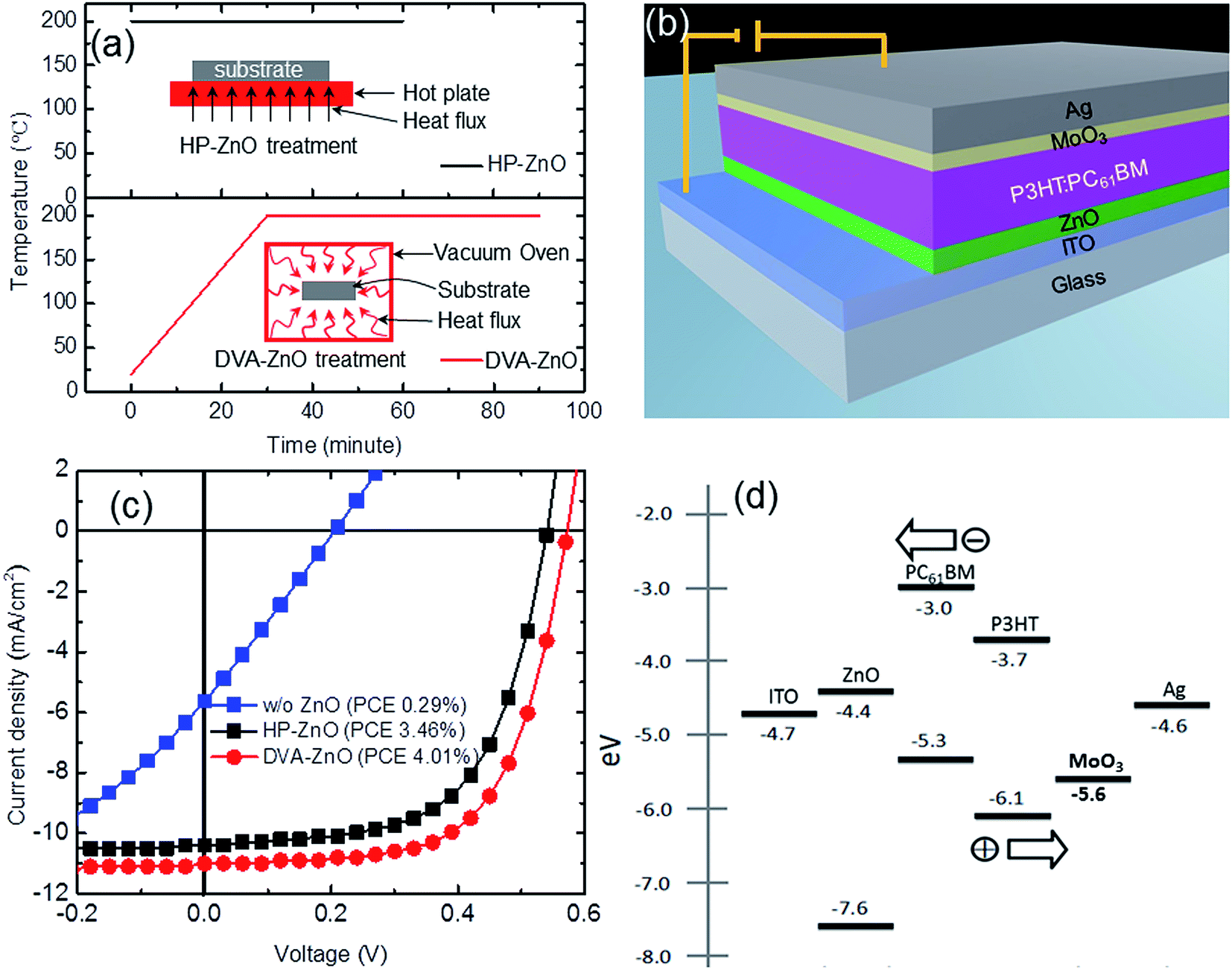 | ||
| Fig. 1 (a) Two kind of low temperature annealing conditions for the sol–gel ZnO films. (b) The device structure of the inverted P3HT:PC61BM solar cell. (c) J–V characteristic of IPSCs with different sol–gel ZnO annealing condition. (d) Energy level diagram of the component materials used in device fabrication. | ||
The J–V characteristics of the IPSCs without a ZnO layer, with an HP-ZnO layer, and with a DVA-ZnO layer under simulated AM 1.5G solar irradiation are shown in Fig. 1(c), and the values are summarized in Table 1. Reference devices without ZnO exhibited a Voc, Jsc, FF and PCE of 0.21 V, 5.63 mA cm−2, 25%, and 0.29%, respectively. The device performance was ascribed to the poor ohmic contact between ITO and P3HT:PC61BM, which restricted the electron collection. The device based on HP-ZnO exhibited performance with a Jsc of 10.51 mA cm−2, Voc of 0.54 V, FF of 61%, and PCE of 3.46%. The overall enhancement of device performance revealed the positive effect arising from ZnO incorporation, which was associated with the modification of the work-function of ITO by coating a ZnO layer, which lead to effective electron transport and collection in devices. As shown in Fig. 1(d), the work function of ITO is 4.7 eV. After modification of ZnO ETL, the work function was reduced to 4.4 eV,24 which is closer to the lowest unoccupied molecular orbital (LUMO) energy level (4.2 eV) of PC61BM. In comparison, the DVA-ZnO-based device with 20 nm thickness had an enhanced performance with a Jsc of 11.11 mA cm−2, Voc of 0.57 V, FF of 63%, and PCE of 4.01%. The enhancement of FF was derived from the increase in Rsh and the decrease in Rs, which were 1338 Ω cm2 and 6.7 Ω cm2, respectively. There was a 15.9% enhancement in PCE, which could be attributed to the improved interface properties between ZnO and the photoactive layer. The optimized post-annealing process of ZnO improved the charge carrier transport and recombination at the ZnO and P3HT:PC61BM interface.
| Annealing | Voc (V) | Jsc (mA cm−2) | FF (%) | PCE (%) | Rs (Ω cm2) | Rsh (Ω cm2) |
|---|---|---|---|---|---|---|
| Best (averagea) | ||||||
| a Average PCEs were based on ten devices. The Rsh and Rs were calculated by the inverse of the slope of the corresponding J–V curves under illumination at V = 0 and J = 0, respectively. | ||||||
| w/o ZnO | 0.210(0.200 ± 0.010) | 5.63(5.51 ± 0.12) | 25.0(25.0 ± 0.1) | 0.29(0.25 ± 0.05) | 34.6(35.10 ± 0.50) | 41.3(40.10 ± 1.20) |
| HP-ZnO | 0.540(0.536 ± 0.004) | 10.51(10.41 ± 0.10) | 61.0(60.8 ± 0.2) | 3.46(3.40 ± 0.08) | 8.9(8.65 ± 0.30) | 1157(1126.00 ± 29.00) |
| DVA-ZnO | 0.570(0.566 ± 0.004) | 11.11(10.81 ± 0.10) | 63.0(63.8 ± 0.4) | 4.01(3.70 ± 0.11) | 6.7(7.02 ± 0.32) | 1338(1313.00 ± 40.00) |
For all the inverted devices investigated in this study, the tuning parameters are the morphology and thickness of the ZnO cathode buffer layer. All the other aspects, including the chemical composition and other layers of the device, were controlled to be exactly the same as far as the lab facilities permit. Here, two sets of ZnO layers were fabricated to investigate the influence of the thickness on the photovoltaic performance of the device. Fig. 2(a–d) shows the electrical parameters of the IPSCs with various thicknesses of HP-ZnO and DVA-ZnO layers. The photovoltaic performance was found to be dependent on the thickness of the ZnO film. As shown in Fig. 2(a), devices with HP-ZnO films showed dependence on ZnO thickness. With increasing ZnO thickness, the average Voc, Jsc, FF, and PCE increased first and then decreased. For DVA-ZnO-based devices, the average Voc, FF, and PCE increased first and then remained stable. It was found that IPSCs with a rough ZnO were more sensitive to device performance, which demonstrated that surface trapping state, recombination loss of charge carriers, and leakage current varied with increasing ZnO thickness. Meanwhile, when comparing these two sets of devices, the IPSCs based on DVA-ZnO exhibited overall higher Voc, FF, and PCE than HP-ZnO-based IPSCs. The average power-conversion efficiency of DVA-ZnO-based devices was 3.7%, while devices based on HP-ZnO showed a PCE of 3.4%. The improved performance indicated that DVA-ZnO effectively facilitated the electron transport and collection, and restricted the charge recombination in solar cell devices.35
 | ||
| Fig. 2 (a–d) The thickness dependence of Voc, Jsc, FF and PCE of IPSCs based on HP-ZnO and DVA-ZnO. | ||
3.2 Film morphology of ZnO film
The surface morphology of the HP-ZnO and DVA-ZnO films on top of ITO by AFM images was measured to investigate the effect of the annealing processes. AFM images of the nano-ridge and planar films are shown in Fig. 3(a and b), respectively. Obviously, the surface morphology of the DVA-ZnO film was smoother than that of the HP-ZnO film. The root mean square (RMS) roughness of the DVA-ZnO film decreased from 2.5 nm to 0.7 nm with increasing spin-coating speed. The RMS roughness of the HP-ZnO film ranged from 20.8 to 2.3 nm. The smoother morphology could be the reason for the increased performance of IPSCs. It can be seen that the rough morphology resulted in a film defect and narrow nano-valleys between the nano-ridges. During the solvent annealing process of the active layer, it is likely that part of the solution was unable to penetrate to the bottom of the valley, leading to the formation of defects. This could, in turn, lead to a higher contact resistance and carrier recombination.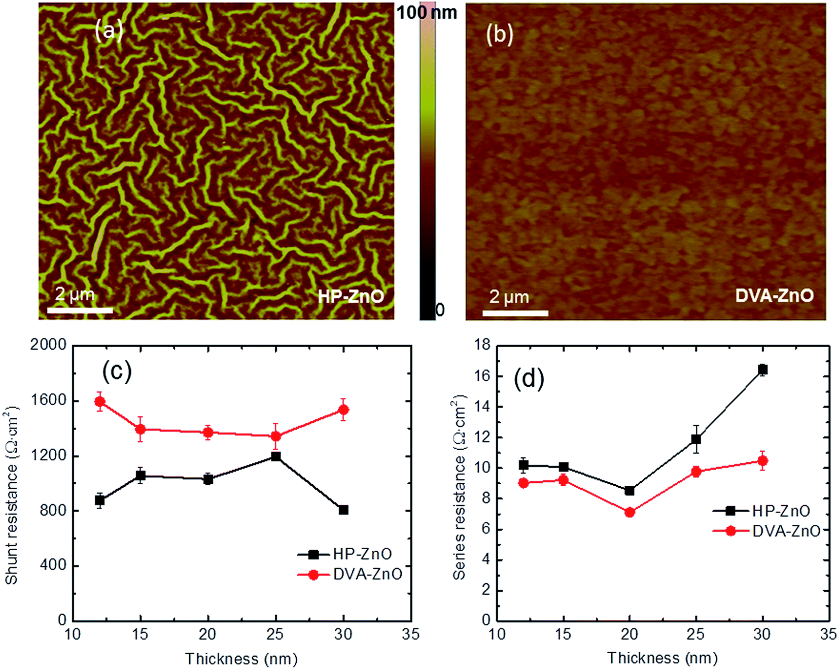 | ||
| Fig. 3 AFM images of ZnO films with the following annealing method: (a) 200 °C hot plate annealing for 60 min. (b) 200 °C vacuum oven annealing for 90 min. (c) Shunt resistance–thickness characteristic of IPSCs. (d) Series resistance–thickness characteristic of IPSCs. | ||
The contact between the ZnO layer and P3HT:PC60BM active layer had a significant impact on the series resistance (Rs) and shunt resistance (Rsh) of the IPSCs. It has been reported that the contact resistance and charge recombination at the interface are the major factors that give rise to the increase in Rs while the leakage current leads to the drop of Rsh, respectively.36 The Rsh and Rs of the two sets of devices with the ZnO ETL derived from different annealing process are shown in Fig. 3(c and d). When comparing HP-ZnO and DVA-ZnO, the average Rsh increased from 1032 Ω cm2 to 1371 Ω cm2. Meanwhile, the average Rs decreased from 8.7 Ω cm2 to 6.9 Ω cm2. The increased Rsh with DVA-ZnO could arise from the improved uniformity of the P3HT:PC61BM active layer on the surface of ZnO. On the other hand, the decreased Rs indicates that the electron collection and transportation benefited from the high-quality contact between the P3HT:PC61BM active layer and the amorphous ZnO. As a result, the decreased Rs and increased Rsh contributed to the device performance by improving the FF and Jsc.37,38
3.3 Detailed analysis of device performance
The J–V characteristics of the IPSCs with HP-ZnO and DVA-ZnO under illumination intensities are shown in Fig. 4(a and b). To gain a deeper insight into the influence of the ZnO layer on the electrical properties of the cells, the recombination mechanism of the IPSCs with the HP-ZnO and DVA-ZnO layers was studied by measuring Jsc at various light intensities from 20 mW cm−2 to 100 mW cm−2. A power law dependence of Jsc upon illumination intensity is generally observed in organic solar cells, and can be expressed as:| Jsc ∝ Iα | (1) |
 | ||
| Fig. 4 J–V characteristics of ITO/ZnO/P3HT:PC61BM/MoO3/Ag under illumination at varying light intensities. (a) IPSCs based on hot plate annealed ZnO. (b) IPSCs based on DVA-ZnO. (c) Short circuit current–light intensity dependent characteristic based on HP and DVA based ZnO. | ||
To investigate the characteristic time constants of free and trapped carriers in IPSCs, the impedance spectra (IS) of the solar cell was measured. Impedance spectroscopy permits the determination of several electronic parameters to be analyzed, such as charge carrier lifetime.41,42 Through an equivalent circuit model, the bulk heterojunction can be described as a pair of resistance and capacitance connected in parallel, and the characteristic time constant under open circuit conditions is equal to recombination time constant of the charge carriers. Fig. 5 shows a typical Nyquist plot of IPSCs based on HP-ZnO and DVA-ZnO. From the IS measurements, it can be calculated that the free charge carrier has an effective lifetime of 2.7 μs for the DVA-ZnO device, which is clearly higher than the lifetime of the HP-ZnO device (1.09 μs). The longer lifetime indicated a lower recombination rate, which means a better chance that carriers could reach the electrodes. This is consistent with the improved PCE, as clearly shown in the J–V characteristic under illumination in Fig. 1(c). The resistance decreases prominently with DVA-ZnO, suggesting suppressed charge recombination in the device.
 | ||
| Fig. 5 Impedance spectra of IPSCs measured in dark and light with HP and DVA based ZnO films. | ||
4. Conclusions
In summary, IPSCs were fabricated using a DVA-based method with low-temperature sol–gel ZnO as the ETL. The effect of film thickness and morphology of the ZnO ETL was investigated. Improved photovoltaic properties were observed from the device with a smooth ZnO film. The device fabricated with a DVA-ZnO film of 20 nm and at 200 °C showed the highest PCE (4.01%) compared with the device based on HP-ZnO. The enhancement was studied by measuring the morphology of ZnO films, light intensity dependence, and impedance spectroscopy. The surface morphology of DVA-ZnO was smoother than that of HP-ZnO, which led to fewer surface defects and improved P3HT:PC61BM penetration. Furthermore, the increased Rsh and decreased Rs of DVA-ZnO-based IPSCs directly demonstrated the improved electron transportation and carrier recombination. The device with DVA-ZnO exhibited weak recombination in the device compared with HP-ZnO-based IPSCs when using light intensity dependence measurements. A longer carrier lifetime was found in DVA-ZnO-based IPSCs, while impedance spectroscopy measurements also provided evidence of the weak recombination in IPSCs using DVA-ZnO. The DVA could potentially be used as an efficient method for film fabrication in solar cell devices.Acknowledgements
The authors gratefully acknowledge the financial support from the Young Scholars Development Fund of SWPU (Grant No. 201699010017).References
- F. C. Krebs, Sol. Energy Mater. Sol. Cells, 2009, 93, 394–412 CrossRef CAS.
- G. Li, R. Zhu and Y. Yang, Nat. Photonics, 2012, 6, 153–161 CrossRef CAS.
- J. S. Yu, Y. F. Zheng and J. Huang, Polymer, 2014, 6, 2473–2509 Search PubMed.
- J. F. Zhu, X. D. Zhu, R. Hoekstra, L. Li, F. X. Xiu, M. Xue, B. Q. Zeng and K. L. Wang, Appl. Phys. Lett., 2012, 100, 143109 CrossRef.
- Q. Gan, F. J. Bartoli and Z. H. Kafafi, Adv. Mater., 2013, 25, 2385–2396 CrossRef CAS PubMed.
- Z. C. He, B. Xiao, F. Liu, H. B. Wu, Y. L. Wu, Y. L. Yang, S. Xiao, C. Wang, T. P. Russell and Y. Cao, Nat. Photonics, 2015, 9, 174–179 CrossRef CAS.
- N. J. Zhou, D. B. Buchholz, G. Zhu, X. G. Yu, H. Lin, A. Facchetti, T. J. Marks and R. P. H. Chang, Adv. Mater., 2014, 26, 1098–1104 CrossRef CAS PubMed.
- N. N. Wang, J. S. Yu, Y. Zang, J. Huang and Y. D. Jiang, Sol. Energy Mater. Sol. Cells, 2010, 94, 263–266 CrossRef CAS.
- X. N. Zhang, S. Yang, S. Q. Bi, A. Kumaresan, J. Y. Zhou, J. Seifter, H. Y. Mi, Y. Xu, Y. Zhang and H. Q Zhou, RSC Adv., 2017, 7, 12400 RSC.
- H. Hoppe and N. S. Sariciftci, J. Mater. Res., 2004, 19, 1924–1945 CrossRef CAS.
- Z. G. Yin, J. J. Wei and Q. D. Zheng, Adv. Sci., 2016, 3, 1500362 CrossRef PubMed.
- J. Y. Yuan, W. P. Guo, Y. X. Xia, M. J. Ford, F. Jin, D. Y. Liu, H. B. Zhao, O. Inganas, G. C. Bazan and W. L. Ma, Nano Energy, 2017, 35, 251–262 CrossRef CAS.
- W. C. Zhao, S. S. Li, S. Q. Zhang, X. Y. Liu and J. H. Hou, Adv. Mater., 2017, 29, 164059 Search PubMed.
- M. M. Li, K. Gao, X. J. Wan, Q. Zhang, B. Kan, R. X. Xia, F. Liu, X. Yang, H. R. Feng, W. Ni, Y. C. Wang, J. J. Peng, H. T. Zhang, Z. Q. Liang, H. L. Yip, X. B. Peng, Y. Cao and Y. S. Chen, Nat. Photonics, 2017, 11, 85–90 CrossRef CAS.
- A. R. B. M. Yusoff, D. Kim, H. P. Kim, F. K. Shneider, W. J. da Silva and J. Jang, Energy Environ. Sci., 2015, 8, 303–316 CAS.
- M. Jorgensen, K. Norrman, S. A. Gevorgyan, T. Tromholt, B. Andreasen and F. C. Krebs, Adv. Mater., 2012, 24, 580–612 CrossRef PubMed.
- M. Jorgensen, K. Norrman and F. C. Krebs, Sol. Energy Mater. Sol. Cells, 2008, 92, 686–714 CrossRef.
- M. Glatthaar, N. Mingirulli, B. Zimmermann, T. Ziegler, R. Kern, M. Niggemann, A. Hinsch and A. Gombert, Phys. Status Solidi A, 2005, 202, 125–127 CrossRef.
- T. Stubhan, H. Oh, L. Pinna, J. Krantz, I. Litzov and C. J. Brabec, Org. Electron., 2011, 12, 1539–1543 CrossRef CAS.
- S. K. Hau, H. L. Yip and A. K. Y. Jen, Polym. Rev., 2010, 50, 474–510 CrossRef CAS.
- Z. C. He, C. M. Zhong, S. J. Su, M. Xu, H. B. Wu and Y. Cao, Nat. Photonics, 2012, 6, 591–595 Search PubMed.
- J. B. You, C. C Chen, L. T. Dou, S. Murase, H. S. Duan, S. A. Hawks, T. Xu, H. J. Son, L. P. Yu, G. Li and Y. Yang, Adv. Mater., 2012, 24, 5267–5272 CrossRef CAS PubMed.
- S. Chen, J. R. Manders, S. W. Tsang and F. So, J. Mater. Chem., 2012, 22, 24202–24212 RSC.
- M. S. White, D. C. Olson, S. E. Shaheen, N. Kopidakis and D. S. Ginley, Appl. Phys. Lett., 2006, 89, 143517 CrossRef.
- Z. H. Lin, J. J. Chang, C. Y. Jiang, J. Zhang, J. S. Wu and C. X. Zhu, RSC Adv., 2014, 4, 6646–6651 RSC.
- R. Geethu, C. S. Kartha and K. P. Vijayakumar, Sol. Energy, 2015, 120, 65–71 CrossRef CAS.
- X. D. Zhu, T. Kawaharamura, A. Z. Stieg, C. Biswas, L. Li, Z. Ma, M. A. Zurbuchen, Q. B. Pei and K. L. Wang, Nano Lett., 2015, 15, 4948–4954 CrossRef CAS PubMed.
- Y. M. Sun, J. H. Seo, C. J. Takacs, J. Seifter and A. J. Heeger, Adv. Mater., 2011, 23, 1679–1683 CrossRef CAS PubMed.
- A. K. K. Kyaw, X. W. Sun, C. Y. Jiang, G. Q. Lo, D. W. Zhao and D. L. Kwong, Appl. Phys. Lett., 2008, 93, 221107 CrossRef.
- T. Kuwabaraa, T. Nakashimaa, T. Yamaguchia and K. Takahashi, Org. Electron., 2012, 13, 1136–1140 CrossRef.
- N. Sekine, C. H. Chou, W. L. Kwan and Y. Yang, Org. Electron., 2009, 10, 1437–1477 CrossRef.
- X. Yu, Z. Y. Hu, Z. H. Huang, X. M. Yu, J. J. Zhang, G. S. Zhao and Y. Zhao, Chin. Phys. B, 2013, 22, 118801 CrossRef.
- Z. G. Yin, Q. D. Zheng, S. C. Chen and D. D. Cai, ACS Appl. Mater. Interfaces, 2017, 9(7), 6168–6193 Search PubMed.
- Z. G. Yin, Q. D. Zheng, S. C. Chen and D. D. Cai, ACS Appl. Mater. Interfaces, 2013, 5(18), 9015–9025 CAS.
- H. Ma, H. L. Yip, F. Huang and A. K. Y. Jen, Adv. Funct. Mater., 2010, 20, 1371–1388 CrossRef CAS.
- X. G. Guo, N. J. Zhou, S. J. Lou, J. Smith, D. B. Tice, J. W. Hennek, R. P. Ortiz, J. T. L Navarrete, S. Y. Li, J. Strzalka, L. X. Chen, R. P. H. Chang, A. Facchetti and T. J. Marks, Nat. Photonics, 2013, 7, 825–833 CrossRef CAS.
- D. Gupta, M. Bag and K. S. Narayan, Appl. Phys. Lett., 2008, 92, 093301 CrossRef.
- Z. Q. Liang, Q. F. Zhang, O. Wiranwetchayan, J. T. Xi, Z. Yang, K. Park, C. D. Li and G. Z. Cao, Adv. Funct. Mater., 2012, 22, 2194–2201 CrossRef CAS.
- P. Schilinsky, C. Waldauf, J. Hauch and C. J. Brabec, J. Appl. Phys., 2004, 95, 2816–2819 CrossRef CAS.
- L. J. A. Koster, V. D. Mihailetchi, H. Xie and P. W. M. Blom, Appl. Phys. Lett., 2005, 87, 203502 CrossRef.
- Q. X. Wen, J. Zhuang, Q. G. He, Y. Deng, H. M. Li and J. Guo, RSC Adv., 2015, 5, 91997–92003 RSC.
- Y. Xiang, J. Yu, J. Zhuang, Z. Ma and H. M. Li, Sol. Energy Mater. Sol. Cells, 2017, 165, 45–51 CrossRef CAS.
| This journal is © The Royal Society of Chemistry 2017 |