
 Open Access Article
 This Open Access Article is licensed under a
 Creative Commons Attribution 3.0 Unported Licence
Twinning and its formation mechanism in a binary Mg2Si thermoelectric material with an anti-fluorite structure†
Jeong In Jangab,
Ji Eun Leeb,
Bong-Seo Kimb,
Su-Dong Parkb and
Ho Seong Lee *a
*a
aSchool of Materials Science and Engineering, Kyungpook National University, 80 Daehak-ro, Buk-gu, Daegu 41566, Republic of Korea. E-mail: hs.lee@knu.ac.kr
bKorea Electrotechnology Research Institute, 12 Bulmosan-ro 10 beon-gil, Seongsan-gu, Changwon-si, Gyeongsangnam-do 51543, Republic of Korea
First published on 18th April 2017
Abstract
We investigated twinning and its formation mechanism in a binary Mg2Si thermoelectric material with an anti-fluorite structure. Mg2Si was fabricated via a solid-state reaction using pure Mg and Si and then spark plasma sintered at 50 MPa and 1003 K. Twinning bands, V-shaped twins, three-fold twins, and domains with triple periodicity were observed. The formation of these twins is explained by a self partial-multiplication twinning mechanism associated with partial dislocations and stacking faults similar to those in face-centered cubic pure metals. These results provide insight into the microstructural properties of Mg2Si thermoelectric materials, which will help to improve their figure-of-merit.
1. Introduction
Thermoelectric materials are attractive because they can generate useful electricity from waste heat. The improvement of the thermoelectric conversion efficiency strongly depends on increasing the dimensionless figure-of-merit, ZT = S2σT/κ, where S is the Seebeck coefficient, σ is the electrical conductivity, T is the absolute temperature, and κ is the thermal conductivity.1–3Telluride derivatives such as Bi2Te3,4–6 PbTe,7,8 and GeTe9,10 have been considered the best thermoelectric materials for the past several decades. Using these Telluride derivatives with high ZT values provides advantages such as higher energy conversion efficiency compared to using other thermoelectric materials. A large ZT value is partially associated with a low thermal conductivity. However, these materials also possess certain disadvantages such as toxicity, rarity, and high cost. Therefore, alternatives consisting of elements that are nontoxic, abundant, and inexpensive are needed. In this respect, Mg2Si-based materials may be promising candidates.11–13 A large improvement of the performance of bulk Mg2Si-based thermoelectric materials can be achieved by forming a solid solution by partially replacing Si with Ge or Sn and through band convergence by doping with Sb.14–17
The grain boundaries in thermoelectric materials are critical because they can scatter electronic carriers and phonons.18 High-density embedded nanointerfaces can increase phonon scattering, leading to a reduction of the thermal conductivity.19 The twin boundary can be a simple grain boundary. The {111} twins in Si exhibit a low potential barrier and low electronic activity for electronic transport that are less than those for a random-oriented boundary.20 In addition, high-density twinning in the thermoelectric compound (AgSbTe2)15(GeTe)85 (TAGS85) can scatter mid and long wavelength phonons, resulting in reduction of thermal conductivity.21 These twinning behaviors may be favorable for improvement of the ZT value because an interface is needed to scatter phonons without degrading electronic transport.
In this study, we observed twinning in Mg2Si for the first time and investigated several types of twinning. To refine their grain size and control their crystallographic textures to achieve optimal electronic and thermal transport, Mg2Si-based thermoelectric materials undergo a significant amount of deformation during processing. In this case, we assumed that twins can be formed by shear deformation even though growth and annealing twins can also be generated in spark plasma sintered nanocrystalline Mg2Si.
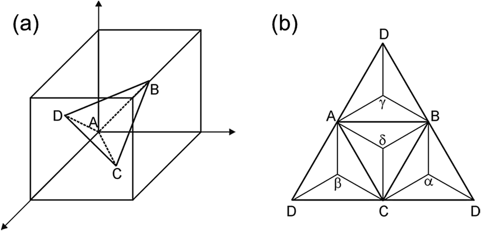
Face-centered cubic (fcc) Mg2Si has an anti-fluorite structure with a lattice parameter of a = 0.6338 nm and a point group of Fm3m.22 This structure contains three atoms per lattice point, with four chemical formula units per unit cell. Si atoms occupy the (0 0 0) position and lattice points, and Mg atoms occupy (1/4 1/4 1/4), (1/4 3/4 1/4), and equivalent positions, as illustrated in Fig. 1(a). Si is surrounded by nearest neighboring Mg atoms arranged in a cubic apex with a coordination number of eight. The center type of atom forms the net of an equitriangular point parallel to the {111} lattice planes, as illustrated in Fig. 1(b). The stacking order of these planes is…αBγ βCα γAβ αBγ βCα γAβ…, where the Si atomic planes represented by the sequential Roman characters are spaced at a uniform separation distance.23 The Mg atomic planes represented by Greek characters have a constant atomic planar distance.
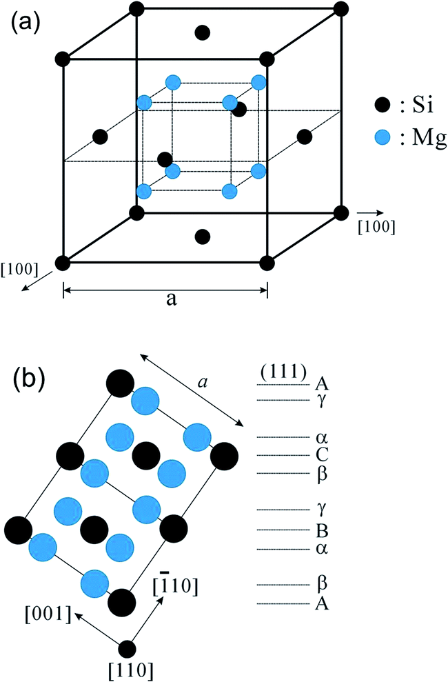 | ||
| Fig. 1 Schematic diagrams of (a) fcc Mg2Si with an anti-fluorite structure and (b) projection of atomic arrangement in the [110] direction. The stacking order of {111} planes is…αBγ βCα γAβ αBγ βCα γAβ…, where the Si and Mg atomic planes are represented by sequential Roman and Greek characters, respectively. | ||
Perfect dislocations, stacking faults, and twins in fcc crystals are all associated with the {111} planes.24 However, the detailed structures of these defects are very different. A perfect dislocation is a line defect that does not change lattice direction when gliding. Shockley partial dislocations generate stacking faults as they glide. These stacking faults are planar defects and change fcc stacking sequences. A twin is also a planar defect but is composed of at least two neighboring stacking faults. These stacking faults reorient the lattice and produce a twin boundary. As a result, these defects do not induce the same microstructure, slip activity, or deformation reaction for the same strain rate.
2. Experimental details
A Mg2Si thermoelectric material was synthesized by a solid-state reaction (SSR) combined with spark plasma sintering. High-purity Mg (99.6%, Alfa Aesar) and Si (99.9985%, Alfa Aesar) in the form of fine powders were weighed according to their nominal compositions. An excess of Mg of approximately 10% over the stoichiometric composition was added to compensate for its Mg resulting from the high evaporation rate during the synthesis process. The powders were mixed and hand-grinded in an agate mortar before being cold pressed into pellets. They were then sealed in quartz tubes under vacuum. The grinding and mixing process were performed in a glove box to prevent oxidation. The SSR was performed at 873 K. The as-synthesized pellets were crushed and pulverized by hand milling with agate mortar and pestle for 1 h. The particle size of pulverized powder was distributed from 1 μm to 10 μm (see Fig. SI1, ESI†). Then, spark plasma sintering was performed at 1003 K and 50 MPa for 15 min in an Ar atmosphere using commercial equipment (SPS-515s, SPS Syntex Inc). Heating rate was fast (100 K min−1) in early stage and reduced gradually to avoid overheating (100 K min−1 to 903 K, 50 K min−1 to 953 K, 20 K min−1 to 973 K, and 10 K min−1 to 1003 K). The resultant pellet density was approximately 99% of the theoretical density.Transmission electron microscopy (TEM) specimens were cut using a diamond saw, mechanically polished to less than 30 μm, and finally ion milled using a precision ion polishing system (PIPS 691, Gatan). The accelerating voltage and current were 4.0 kV and approximately 10 mA, respectively, and the ion beam was aligned at an angle of 6°. The specimens were also investigated using TEM (Titan G2 ChemiSTEM Cs probe, FEI) with a Cs-corrector probe.
3. Results and discussion
Fig. 2(a) presents a bright-field TEM micrograph of the Mg2Si thermoelectric material showing several particles with sizes in the range of several hundred nanometers to several micrometers. Many black lines are observed in the larger particle, indicating that many twin bands were formed. Fig. 2(b) presents a selected area electron diffraction (SAED) pattern of the large particle. Both weak diffraction spots and the strong main diffraction spots were observed. The typical twinning diffraction spots of fcc crystal structures appeared as weak diffraction spots at the location of 1/3 along the 〈111〉 directions with mirror symmetry along the [111] rotation axis,25 which is in reasonable agreement with the result shown in Fig. 2(c). According to the SAED pattern analysis of the twins, the twin orientation relationship was (111)M//(111)T and [110]M//[110]T, where M and T represent the matrix and twin, respectively. The habit plane of the twin is parallel to the (111) plane. The close-packed plane and direction of the two crystals in the habit plane were reoriented. Fig. 2(c) presents a high-resolution TEM (HRTEM) micrograph corresponding to Fig. 2(b), which confirmed that many twin bands were formed and that the twinning plane was the (111) plane.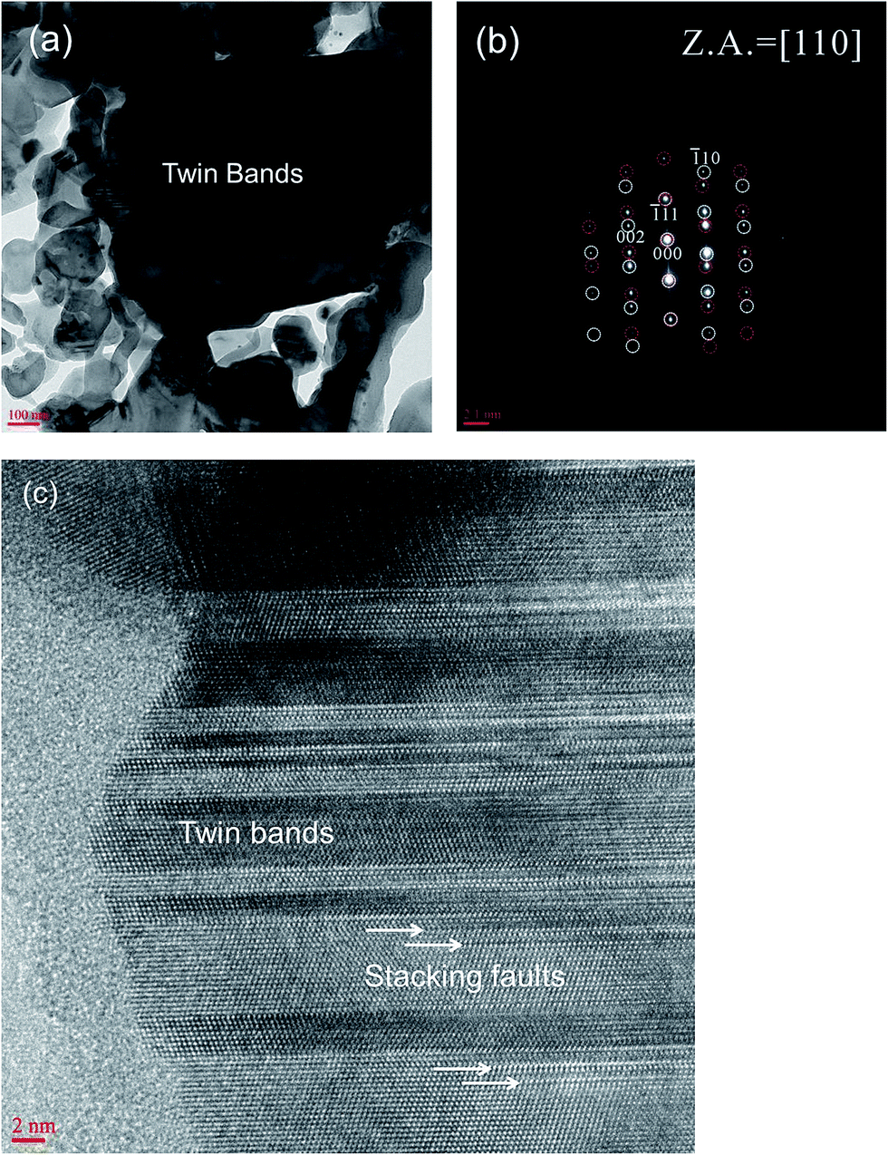 | ||
| Fig. 2 (a) Bright-field TEM micrograph obtained from Mg2Si thermoelectric material and (b) corresponding SAED pattern. The diffraction spots indicated by white and red circles correspond to the matrix and twin, respectively. (c) HRTEM micrograph showing the twin bands and stacking faults. | ||
The crystallographic feature of twinning is mirror symmetry of the atomic arrangement along the twin boundary.26 This symmetry in fcc materials is observed well along the [110] direction on the coherent twin plane. As observed in Fig. 3, the coherent twin plane is a (1![[1 with combining macron]](https://www.rsc.org/images/entities/char_0031_0304.gif) ) close-packed plane, and the angle between the other close-packed planes is 70.53°. In a two-dimensional figure, each atomic point contains a row of atoms. The mirror symmetry in a HRTEM micrograph is used to confirm twinning in fcc materials.
) close-packed plane, and the angle between the other close-packed planes is 70.53°. In a two-dimensional figure, each atomic point contains a row of atoms. The mirror symmetry in a HRTEM micrograph is used to confirm twinning in fcc materials.
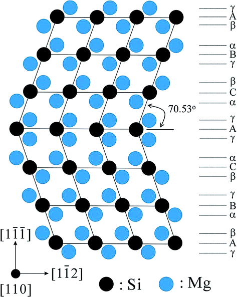 | ||
| Fig. 3 Schematic diagram of a regular twin in Mg2Si with an anti-fluorite structure. To maintain the integrity of the lattice, a twin such as…αBγ βCα γA γ αCβ γBα…is formed. | ||
There are several microstructural possibilities for the stacking sequence of a twin in the Mg2Si structure. Designating the Mg and Si layers by Greek and Roman letters, respectively, we can describe the close-packed stacking {111} plane of the Mg2Si structure as…αBγ βCα γAβ αBγ βCα γAβ…. The twins in the Mg2Si structure can be described in one of the following four ways:
Twin 1:…αBγ βCα γ![[A with combining low line]](https://www.rsc.org/images/entities/char_0041_0332.gif) γ αCβ γBα…
γ αCβ γBα…
Twin 2:…αBγ βC Cβ γBα…
Twin 3:…αBγ βC
 Cβ γBα…
Twin 4:…αBγ βC αCβ γBα…
Here, the underline represents the twin plane. All of these twins exhibit mirror symmetry. However, in twin 3, the planes α–α or A–A meet directly above the same plane without atomic displacement. The planes α–α or A–A are located at the high-energy position; thus, this arrangement is expected to be associated with higher energy than any other configuration. Twin 4 has a sequence of -α γ α-. These three layers consisted of only Mg atoms. The Mg2Si crystal is considered to be more stable when both sides of the γ plane are surrounded by different types of atomic planes. Thus, twin 4 is expected to be unstable. In twin 3, the lattice is not conserved at the twin boundary. Twin 1 maintains the integrity of a lattice; however, at the twin boundary, the lattice is reoriented. In this respect, twin 1 is the most stable. Fig. 3 was drawn based on this consideration.
Fig. 4(a) presents another bright-field TEM micrograph. Many lines and domains with black contrast are observed in the nanoparticle. The black lines represent twin bands, and the black domains indicated by “A” and “B” correspond to regions with triple periodicity of the atomic planes, as will be described below. Specific angles of 70.5° or 109.5° are formed between the black straight lines; these angles correspond to those between the {111} planes. Some Moiré fringes indicated by region “C” are also observed. Fig. 4(b) is a SAED pattern corresponding to the bright-field TEM micrograph presented in Fig. 4(a). Several weak diffraction spots as well as the main diffraction spots are observed. The red and yellow arrows correspond to the matrix and twinning, respectively, and mirror symmetry is observed along the (111) plane. The spots labeled by the triangles are not spots from the matrix or twins but originate from the triple periodicity of the {111} planes. This finding was confirmed by the HRTEM results in Fig. 6 These spots were observed at positions of 1/3 and 2/3 from the main spots along the [111] direction. Some spots were overlapped by twinning spots. Regions “A” and “B” regions in Fig. 4(a) exhibit the triple periodicity of (111) planes.
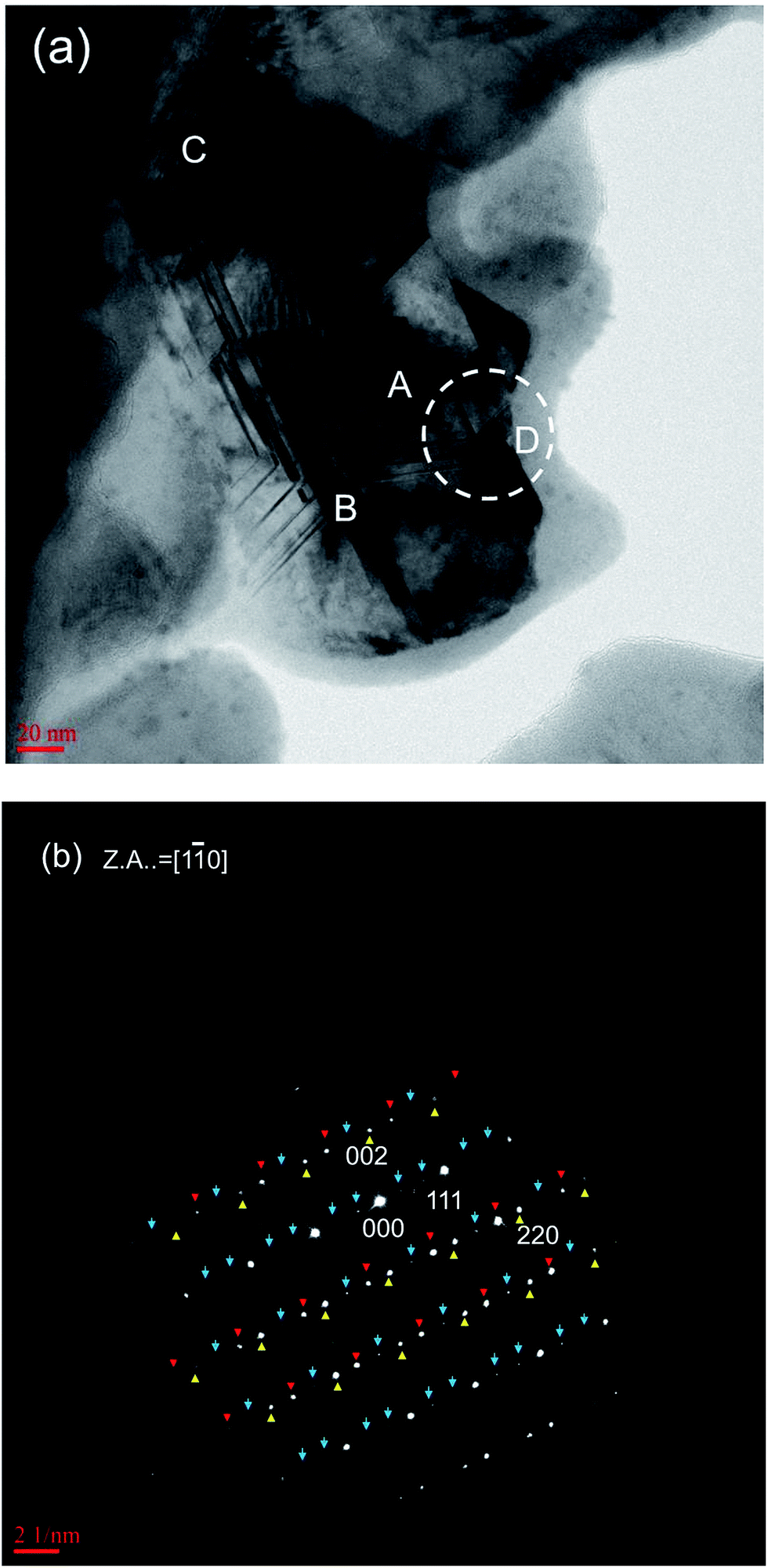 | ||
| Fig. 4 (a) Bright-field TEM micrograph obtained from Mg2Si thermoelectric material showing several domains. (b) Corresponding SAED pattern showing the main strong spots as well as regular weak spots. The spots labeled with red and yellow triangles have a twinning relation, and the spots labeled by blue arrows show triple periodicity along the [111] direction. | ||
Fig. 5 presents a HRTEM micrograph corresponding to region “B” in Fig. 4. Multiple twin bands are observed in the left-hand region; some regions also contain stacking faults; and regular or irregular triple periodicities are clearly observed in the right-hand region. These features are all considered to be partially related to the pile-up of partial dislocations or sessile dislocations and stacking faults of (111) planes.27 A step of multiple twin bands resulting from the pile-up of partial dislocation is also observed, as indicated by the white dotted circle. Zigzag contrast is also observed due to the crossing of multiple twin bands of the right- and left-hand side, as shown in Fig. 4(a).
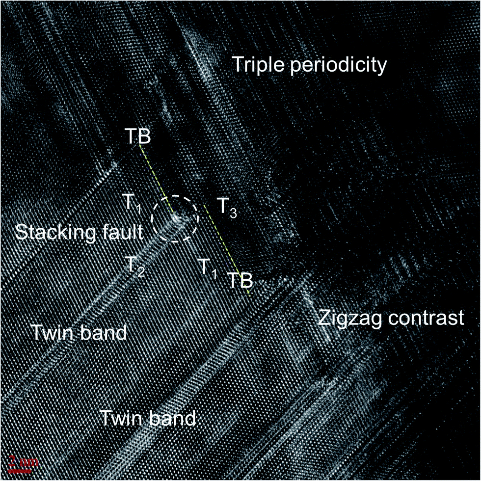 | ||
| Fig. 5 HRTEM micrograph corresponding to region “B” in Fig. 4. Twin bands, stacking faults, triple periodicity, and zigzag contrast are observed. The labels T1, T2, and T3 indicate twins with different variants, and the label TB indicates a twin boundary. | ||
Fig. 6(a) presents a HRTEM micrograph corresponding to circled region “D” in Fig. 4(a). A multiple twin band in the middle region and triple periodicity at the left-side are observed. The interesting triple joint twinning is also observed in the right region. The inverse masked fast Fourier transforms (FFTs) are shown in Fig. 6(b). The atomic arrangement corresponding to the triple variant (T1, T2, T3) is observed. The twin boundaries between T2 and T3 and T1 and T3 form Σ3 coincidence site lattices.28 However, the twin boundary between T1 and T2 does not exhibit lattice coincidence. This structure was considered to accommodate the elastic strain generated by the lattice mismatch. A schematic diagram is presented in Fig. 7.
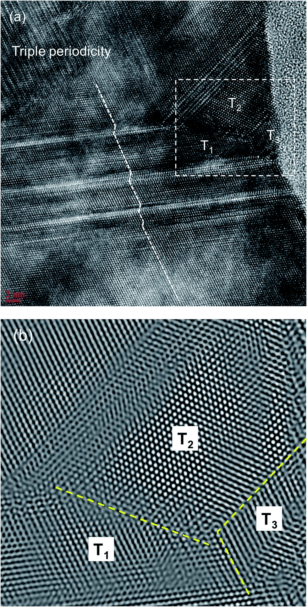 | ||
| Fig. 6 (a) HRTEM micrograph corresponding to region “D” in Fig. 4. Triple periodicity and a threefold twin are observed. (b) Inverse FFT micrograph corresponding to the region indicated by the dotted square in (a). | ||
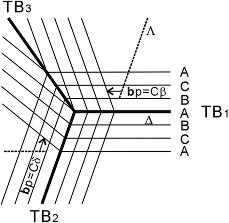 | ||
| Fig. 7 Schematic diagram of a threefold twin. The lines indicated by “Δ” and “Λ” represent {111} planes. bp indicates a partial dislocation. | ||
There are four different sets of {111} slip planes in fcc metals. These geometrical relations are described by the Thompson tetrahedron shown in Fig. 8(a).27 The angle between two slip planes is 70.53°. The four different sets of {111} planes lie parallel to the four faces of a regular tetrahedron and can be described by the equilateral triangles BCD, ACD, ABD, and ABC shown in Fig. 8(b). The edges of the tetrahedron are parallel to 〈110〉 and represent the Burgers vector of a perfect dislocation, 1/2〈110〉. Points α, β, γ, and δ are located at the centers of these triangles. The Burgers vectors 1/2〈110〉 of perfect dislocations are described in both magnitude and direction by the edges of the tetrahedron and will be BC, AC, etc. The Burgers vectors 1/6〈112〉 of a Shockley partial dislocation is indicated by the line from the corner to the center of a face, such as Aβ, δC, etc. The Burgers vector βδ of a stair-rod partial dislocation is perpendicular to the dislocation line and does not lie in the slip planes; thus, it cannot glide.
 | ||
| Fig. 8 (a) Thompson tetrahedron and (b) its two-dimensional representation. | ||
Several types of multiple twins are often observed in nanocrystalline Cu,29 Al,30 Ni,31 Pd,32 and other fcc metals and alloys.33 However, their nucleation and growth mechanism remain unclear. The formation mechanism of a twin in a Mg2Si crystal can be explained by the self partial-multiplication twinning mechanism suggested by Y. T. Zhu et al.26,27 without any special assumptions. A pure fcc metal and binary Mg2Si have the same lattice structure but a different motif; Mg2Si has three atoms per lattice point.
In Fig. 9, let the line AC be perpendicular to the paper by rotating the Thompson tetrahedron. The planes ABC and ACD become the lines indicated by “Δ” and “Λ”, respectively, as shown in Fig. 9(a). Assume that a Shockley partial dislocation Cβ is present in plane Λ. The partial dislocation Cβ can be dissociated into a partial dislocation Cδ on plane Δ and a stair-rod dislocation δβ:
| Cβ → Cδ + δβ. | (1) |
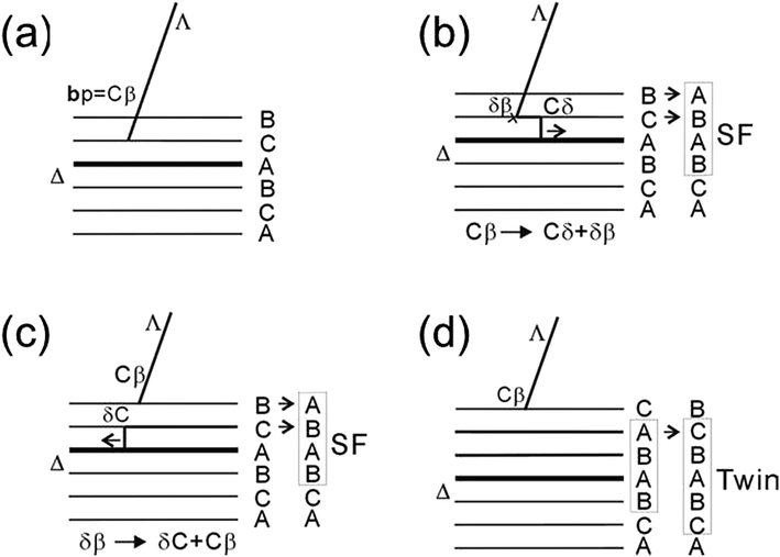 | ||
| Fig. 9 Schematic diagrams showing reaction between a partial dislocation and stacking fault. (a) Partial dislocation bp = Cβ on (11) plane indicated by “Λ”. (b) Dissociation of partial dislocation bp = Cβ into Cδ and δβ, causing the formation of a stacking fault. (c) Dissociation of partial dislocation δβ into δC and Cβ, causing expansion of a stacking fault. (d) Repetition of these reactions results in thickening of the twin. | ||
According to Fig. 9(b), the partial dislocation Cδ glides to the right-hand side and generates a stacking fault, leaving the stair-rod dislocation δβ behind. The stair-rod dislocation δβ can be further dissociated into a partial dislocation δC on plane Δ and a partial dislocation Cβ on plane Λ:
| δβ → δC + Cβ. | (2) |
This reaction is feasible under the large deformation stress associated with spark plasma sintering. According to Fig. 9(c), the partial dislocation δC slips to the left-hand side and extends a stacking fault. The partial dislocation Cβ glides above on plane Λ by one atomic plane distance. The sequential dislocation reaction and movement described by the above multiplication model produce a double-layer twin and leave the original dislocation Cβ behind at the twin boundary. When the partial dislocation Cβ continues to react and the resulting dislocations slip, each reaction cycle causes the twin to grow by one slip plane distance, as observed in Fig. 9(d).
The formation mechanism of V-shaped twins can be explained by extending the above explanation. A partial dislocation is next to a stacking fault. If stress is applied, the partial dislocation Cβ can be dissociated as follows:
| Cβ → CA + Aδ + δβ. | (3) |
The partial dislocation Aδ glides to the right-hand side and generates a twinning nucleus on plane Δ. However, the perfect dislocation CA cross-slips to the intersection of planes ABC and Λ. The stair-rod dislocation δβ cannot move because of its sessile characteristic. The dislocation reaction in eqn (3) is not energetically favorable. Thus, the process occurs under an applied stress. The perfect dislocation CA can be dissociated into two partial dislocations Cβ and βA:
| CA → Cβ + βA. | (4) |
The partial dislocation βA glides above, produces a twin on plane Λ, and forms the nucleus of a V-shaped double twin. The partial dislocation Cβ can repeat the above dislocation reaction and process. A stair-rod dislocation δβ exists at every intersection of plane Δ and Λ, which induces a large stress at the end of stair-rod pile-ups at the intersection boundary of two twins, as shown in Fig. 5.
Triple-deformation twinning formation has been explained by the sequential twinning formation mechanism of Shockley partial dislocations emitted from twin and grain boundaries.34 However, in this paper, triple-deformation twinning formation will be described by modifying the self partial-multiplication twinning process without requiring multiplication sources in a grain or additional dislocation sources from a grain boundary.26,27
In the following discussion, for convenience, assume that the partial dislocation lines are parallel to the [10] direction. The two planes (11) and ( 11) are represented by the lines “Δ” and “Λ”, respectively, in Fig. 7. Assume that the Shockley partial dislocation bp = Cβ on plane Λ in the twin boundary exists on the TB1 slip plane. The partial dislocation Cβ dissociates into a partial dislocation Cδ on plane Δ and a stair-rod dislocation δβ by shear stress induced by the spark plasma sintering process:
| Cβ → Cδ + δβ. |
The partial dislocation Cδ moves to the right-hand side and forms a stacking fault. The stair-rod dislocation δβ can be separated into a partial dislocation δC on plane Δ and a partial dislocation Cβ on plane Λ.
| δβ → δC + Cβ |
The partial dislocation δC moves to the left-hand side and expands the stacking fault. The partial dislocation Cβ shifts upward by one atomic plane distance. If the above dislocation reactions and slips on the stacking fault occur repeatedly, the consecutive stacking fault forms a twin, and each reaction cycle allows the twin to grow by one slip plane distance. According to this formation mechanism, a simple twin with twinning domains I and II is formed in the twinning boundary TB1.
The above formation mechanism can be directly applied to the Shockley partial dislocation Cδ, which exists in the left plane Δ next to the TB2 slip plane. The Shockley partial dislocation Cδ can be dissociated into a partial dislocation Cβ on the Λ plane and a stair-rod dislocation βδ:
| Cδ → Cβ + βδ. |
The partial dislocation Cβ moves upward and generates a stacking fault. The stair-rod dislocation βδ can be further dissociated into a partial dislocation βC on plane Λ and a partial dislocation Cδ on plane Δ:
| βδ → βC + Cδ. |
The partial dislocation βC moves downward and expands the stacking fault. The partial dislocation Cδ shifts to the left-hand side by one atomic plane distance. If the above dislocation reactions and slips on the stacking fault occur repeatedly, the consecutive stacking fault forms a twin, and each reaction cycle permits the twin to grow by one slip plane distance. Through this formation mechanism, a simple twin with twinning domains I and III is formed in the twinning boundary TB2.
TB1 and TB2 are coherent twin boundaries and form a Σ3 boundary. However, an incoherent boundary TB3 is formed between domains II and III; this boundary accommodates the strain effect induced by the incoherency and generates a Σ9 boundary. If TB1, TB2, and TB3 are joined at one point, an ideal triple-deformation twin is formed, as demonstrated in Fig. 7.
As a promising material for thermoelectrics, Mg2Si has been researched intensively. However, due to the large melting point difference between constituent elements and the high saturated vapor pressure of Mg, it is very difficult to prepare homogeneous and stoichiometric Mg2Si. Thus, many researches have been mainly focused on various synthetic methods and conditions, including induction melting, zone melting, Bridgman growth and mechanical alloying.35–38 There are few reports concerned about microstructure of Mg2Si. Recently, as interests in microstructure of thermoelectric materials have been increased, there are several studies which report microstructure of Mg2Si.13,39–41 However, numbers of report on microstructure in Mg2Si based alloys is not enough, and detail observation and analysis of the microstructure is still lacking compared to chalcogenide thermoelectric materials. We observed microstructure of Mg2Si in atomic-scale for the first time using Cs-corrected STEM, and hope that this study can be a trigger for new perspective on microstructure of Mg2Si.
The spark plasma sintering method, which had been developed to sinter the metal powder for short time, is the proper way to synthesize the thermoelectric elements of high vapor pressure such as magnesium because it was able to be processed at the relatively low temperature for short duration. Deformation twins are the result of shear stress on the crystal after the crystal has formed. Thus, we think pressure during the sintering is important to formation of twinning.
4. Conclusion
In this work, TEM was used to study the microstructural characteristics of a nanoscale binary Mg2Si material synthesized using SSR combined with spark plasma sintering. The SAED pattern and HRTEM results revealed the formation of a twinning band and three-fold twinning. Triple periodicity along the [111] direction was also observed. We described the possible twinning plane at the twin boundary and explained the formation mechanism of twinning in the binary fcc Mg2Si crystal using the self partial-multiplication twinning process. High shear stress during synthetic processing can generate deformation twins. These twins can scatter mid- and long-wavelength phonons, leading to suppression of the thermal conductivity. Thus, it is considered that twins can be an important factor to reduce the thermal conductivity in Mg2Si-based thermoelectric materials.Acknowledgements
This work was supported by a Korea Institute of Energy Technology Evaluation and Planning (KETEP) grant from the Ministry of Trade, Industry & Energy, Republic of Korea (No. 20162000000910).References
- C. Gayner and K. K. Kar, Prog. Mater. Sci., 2016, 83, 330–382 CrossRef CAS.
- W. Liu, Q. Jie, H. S. Kim and Z. Ren, Acta Mater., 2015, 87, 357–376 CrossRef CAS.
- D. L. Medlin and G. J. Snyder, Curr. Opin. Colloid Interface Sci., 2009, 14, 226–235 CrossRef CAS.
- N. Peranio, O. Eibl, S. Baβler, K. Nielsch, B. Klobes, R. P. Hermann, M. Daniel, M. Albrecht, H. Gorlitz, V. Pacheco, N. Bedoya-Martinez, A. Hashibon and C. Elsasser, Phys. Status Solidi A, 2016, 213, 739–749 CrossRef CAS.
- J. Li, Q. Tan, J.-F. Li, D.-W. Liu, F. Li, Z.-Y. Li, M. Zou and K. Wang, Adv. Funct. Mater., 2013, 23, 4317–4323 CrossRef CAS.
- S. I. Kim, K. H. Lee, H. A. Mun, H. S. Kim, S. W. Hwang, J. W. Roh, D. J. Yang, W. H. Shin, X. S. Li, Y. H. Lee, G. J. Snyder and S. W. Kim, Science, 2015, 348, 109–114 CrossRef CAS PubMed.
- P. Jood, M. Ohta, M. Kunii, X. Hu, H. Nishiate, A. Yamamoto and M. G. Kanatzidis, J. Mater. Chem. C, 2015, 3, 10401–10408 RSC.
- H.-J. Wu, S.-W. Chen, T. Ikeda and G. J. Snyder, Acta Mater., 2012, 60, 1129–1138 CrossRef CAS.
- H. S. Lee, B. S. Kim, C. W. Cho, M. W. Oh, B. K. Min, S. D. Park and H. W. Lee, Acta Mater., 2015, 81, 83–90 CrossRef.
- D. Wu, L. D. Zhao, S. Hao, Q. Jiang, F. Zheng, J. W. Doak, H. Wu, H. Chi, Y. Gelbstein, C. Uher, C. Wolverton, M. Kanatzidis and J. He, J. Am. Chem. Soc., 2014, 136, 11412–11419 CrossRef CAS PubMed.
- M. I. Fedorov and G. N. Isachenko, Jpn. J. Appl. Phys., 2015, 54, 07JA05 CrossRef.
- A. S. Tazebay, S. I. Yi, J. K. Lee, H. Kim, J. H. Bahk, S. L. Kim, S. D. Park, H. S. Lee, A. Shakouri and C. Yu, ACS Appl. Mater. Interfaces, 2016, 8, 7003–7012 CAS.
- W. Liu, X. Tang, H. Li, K. Yin, J. Sharp, X. Zhou and C. Uher, J. Mater. Chem., 2012, 22, 13653–13661 RSC.
- G. S. Polymeris, N. Vlachos, A. U. Khan, E. Hatzikraniotis, C. B. Lioutas, A. Delimitis, E. Pavlidou, K. M. Paraskevopoulos and T. Kyratsi, Acta Mater., 2015, 83, 285–293 CrossRef CAS.
- L. Zheng, X. Zhang, H. Liu, S. Li, Z. Zhou, Q. Lu, J. Zhang and F. Zhang, J. Alloys Compd., 2016, 671, 452–457 CrossRef CAS.
- J. Mao, H. S. Kim, J. Shuai, Z. Liu, R. He, U. Saparamadu, F. Tian, W. Liu and Z. Ren, Acta Mater., 2016, 103, 633–642 CrossRef CAS.
- H. Ning, G. D. Mastrorillo, S. Grasso, B. Du, T. Mori, C. Hu, Y. Xu, K. Simpson, G. Maizza and M. Reece, J. Mater. Chem. A, 2015, 3, 17426–17432 CAS.
- S. Muthiah, J. Pulikkotil, A. K. Srivastava, B. D. Pathak, A. Dhar and R. C. Budhani, Appl. Phys. Lett., 2013, 103, 053901 CrossRef.
- J. de Boor, T. Dasgupta, H. Kolb, C. Compere, K. Kelm and E. Mueller, Acta Mater., 2014, 77, 68–75 CrossRef CAS.
- S. Tsurekawa, K. Kido and T. Watanabe, Philos. Mag. Lett., 2005, 85, 41–49 CrossRef CAS.
- B. A. Cook, M. J. Kramer, X. Wei, J. L. Harringa and E. M. Levin, J. Appl. Phys., 2007, 101, 053715 CrossRef.
- P. Villars and L. D. Calvert, Pearson's Handbook of Crystallographic Data for Intermetallic Phases, ASM International, 2nd edn, 1991 Search PubMed.
- A. Kelly and K. M. Knowles, Crystallography and Crystal Defects, Wiley, 2nd edn, 2012 Search PubMed.
- A. Hunter and I. J. Beyerlein, Acta Mater., 2015, 88, 207–217 CrossRef CAS.
- D. B. Williams and C. B. Carter, Transmission Electron Microscopy, Springer, 1st edn, 1996 Search PubMed.
- Y. T. Zhu, X. Z. Liao and X. L. Wu, Prog. Mater. Sci., 2012, 57, 1–62 CrossRef CAS.
- Y. T. Zhu, J. Narayan, J. P. Hirth, S. Mahajan, X. L. Wu and X. Z. Liao, Acta Mater., 2009, 57, 3763–3770 CrossRef CAS.
- P. Liu, K. Du, J. Zhang, L. Wang, Y. Yue, E. Ma, Y. Zhang, Z. Zhang, M. Chen and X. Han, Appl. Phys. Lett., 2012, 101, 121901 CrossRef.
- Z. H. Cao, L. J. Xu, W. Sun, J. Shi, M. Z. Wei, G. J. Pan, X. B. Yang, J. W. Zhao and X. K. Meng, Acta Mater., 2015, 95, 312–323 CrossRef CAS.
- S. Xue, Z. Fan, Y. Chen, J. Li, H. Wang and X. Zhang, Acta Mater., 2015, 101, 62–70 CrossRef CAS.
- X. Wu, Y. T. Zhu, M. W. Chen and E. Ma, Scr. Mater., 2006, 54, 1685–1690 CrossRef CAS.
- H. Rosner, J. Markmann and J. Weissmuller, Philos. Mag. Lett., 2004, 84, 321–334 CrossRef.
- C. H. Wu, D. M. Aruguete, W. T. Renolds Jr and M. Murayama, Acta Mater., 2014, 75, 180–187 CrossRef CAS.
- Y. T. Zhu, X. Z. Liao and R. Z. Valiev, Appl. Phys. Lett., 2005, 86, 103112 CrossRef.
- Y. Noda, H. Kon, Y. Furukawa, N. Otsuka, I. A. Nishida and K. Masumoto, Mater. Trans. JIM, 1992, 33, 845–850 CrossRef CAS.
- K. Mars, H. Ihou-Mouko, G. Pont, J. Tobola and H. Scherrer, J. Electron. Mater., 2009, 38, 1360–1364 CrossRef CAS.
- M. Akasaka, T. Iida, T. Nemoto, J. Soga, J. Sato, K. Makino, M. Fukano and Y. Takanashi, J. Cryst. Growth, 2007, 304, 196–201 CrossRef CAS.
- M. Riffel and J. Schilz, J. Mater. Sci., 1998, 33, 3427–3431 CrossRef CAS.
- Q. Zhang, J. He, T. J. Zhu, S. N. Zhang, X. B. Zhao and T. M. Tritt, Appl. Phys. Lett., 2008, 93, 102109 CrossRef.
- X. Zhang, H. Liu, Q. Lu, J. Zhang and F. Zhang, Appl. Phys. Lett., 2013, 103, 063901 CrossRef.
- K. Yin, X. Su, Y. Yan, C. Uher and X. Tang, RSC Adv., 2016, 6, 16824–16831 RSC.
Footnote |
| † Electronic supplementary information (ESI) available. See DOI: 10.1039/c7ra00541e |
| This journal is © The Royal Society of Chemistry 2017 |