
 Open Access Article
 This Open Access Article is licensed under a
 Creative Commons Attribution 3.0 Unported Licence
Experimental evidence of electronic polarization in a family of photo-ferroelectrics
Hitesh Borkar ab,
Vaibhav Raoacg,
M. Tomard,
Vinay Guptae,
J. F. Scottf and
Ashok Kumar*ab
ab,
Vaibhav Raoacg,
M. Tomard,
Vinay Guptae,
J. F. Scottf and
Ashok Kumar*ab
aCSIR-National Physical Laboratory, Dr K. S. Krishnan Marg, New Delhi 110012, India. E-mail: ashok553@nplindia.org
bAcademy of Scientific and Innovative Research (AcSIR), CSIR-National Physical Laboratory (CSIR-NPL) Campus, Dr K. S. Krishnan Road, New Delhi 110012, India
cSolar and Alternative Energy, Amity University, Jaipur, Rajasthan 302006, India
dDepartment of Physics, Miranda House, University of Delhi, Delhi 110007, India
eDepartment of Physics and Astrophysics, University of Delhi, Delhi 110007, India
fDepartment of Chemistry and Department of Physics, University of St. Andrews, St. Andrews KY16 ST, UK
gUltrasound Research Institute, Kaunas University of Technology, Barsausko st. 59, Kaunas LT-51368, Lithuania
First published on 23rd February 2017
Abstract
We report a family of ferroelectric materials which exhibit optical control of dielectric constant, polarization, and conductivity at ambient conditions. The evolution of photo-induced charge carriers under illumination of weak monochromatic light of wavelength λ = 405 nm developed electronic polarization that reorients or enhances the ionic polarization in the direction of the applied electric field, hence significantly increasing the net polarization. The presence of electronic polarization in perovskites, especially ABO3 oxides, and the contribution to the ionic polarization, is a matter of debate among ferroelectric community; however, recent experimental evidence proved that electronic polarization contributes to overall polarization in different ways: if it is additive, it will act along the direction of ionic polarization; and if it is subtractive, it will act in the opposite direction. We report a newly developed lead-based ferroelectric family Pb1−x(Li0.5Bi0.5)x(Zr0.2Ti0.8)O3 (PLBZT) for x = 0.3, 0.4, 0.5, which have been successfully synthesized by a conventional solid state reaction route. The X-ray diffraction patterns were recorded at room temperature and refined with Rietveld parameters which confirm its tetragonal structure with P4mm space group symmetry. The Raman spectra, dielectric properties and leakage currents are analyzed. The current conduction mechanisms obey bulk limited Poole–Frenkel model and provide optical dielectric constant similar to theoretical value to lead zirconate titanate.
1. Introduction
Several years ago, V. M. Fridkin proposed mechanisms and related phenomena for possible conversion of light to electricity using bulk ferroelectrics, i.e. “photo-ferroelectrics”.1 In the following decades further development has been taken place on ferroelectric photovoltaic (PV) materials and devices,2,3 mostly centered, however, around the understanding of basic physics. A good recent example of the controversy in assessing electronic contributions (as contrasted with ionic contributions) to ferroelectricity is afforded by the work on K3Fe5F15, where the experiments of Blinc et al.4–6 showed no electronic contribution, but subsequent DFT theory by Yamauchi and Picozzi7 incorrectly inferred an electronic (non-ionic) origin.Photo-ferroics are a particular class of materials where phenomena, the ferroelectric effect and the photoelectric or photovoltaic effect are intimately linked. These two effects are somewhat incompatible in nature since high quality ferroelectrics must be electrical insulators in order to withstand large applied voltages or fields, whereas photovoltaic devices need high open-circuit voltage and short-circuit current. A big advantage of photo-ferroelectrics compared to conventional silicon or organic photovoltaic devices is their directionality: polarization dictates the direction of photocurrents. The photo-ferroic systems develop a complex relation between the ferroelectric phase stability (including domain size and distribution) and photo-response; these photo-generated charge carriers (electrons and holes) in relatively high concentration affect the free energy close to ferroelectric transition (Curie point). The nature and magnitude of phase transition can be significantly altered by the photo-excited electron sub-system.
In general it has been observed that the presence of photo-excited charge carriers considerably changes the polarization hysteresis8 and shifts the ferroelectric phase transition temperature towards lower temperatures.9,10 Photo-assisted polarization hysteresis may increase or decrease depending on screening effects, population of defect centers, trap-filling, and neutralization of depolarization fields. The Curie temperatures (Tc) were considerably lowered as observed long ago in SbSI, and the shifts in Tc were proportional to the carrier concentrations in the matrix.11 The presence of charge carriers may cause structural deformation where the unit cell volume gets affected by generation of charge carriers during the phase transition. The effective permittivity has strong dependence on the concentration of carriers. Readers are referred to V. M. Fridkin's seminal texts for the physical manifestations of the photo-ferroic effect.1,12
Recently Dawber et al.13 explained the possible origin and direction of electronic polarization in perovskite BaTiO3. They proposed the change in the electronic weight due to displacement of central cations and 2p electron orbitals for oxygen ions which in turn modifies the ionic polarization. This effect may be more significant if one can change the electron population by any other means. For example, under illumination of light, a significant amount of photo-generated charge carriers develop in the matrix which notably alters the 2p electron orbitals and hence can produce giant electronic polarization in the direction of ionic polarization. The HoMn2O5 crystal polarization depends on the spin direction, which leads to electronic polarization opposite to the ionic polarization of the system.14 The electronic polarization vector may be in the direction of ionic polarization or in the opposite direction; this depends on the electron transfer contribution, hybridization of electronic orbitals, and spectral weight of electron density. A giant electronic polarization was experimentally observed in molecular ferroelectric crystals; their magnitudes were an order of magnitude higher than the ionic polarization. Kobayashi et al. performed polarization experiments on the organic molecular crystal tetrathiafulvalene p-chloranil (TTF-CA) that showed giant electronic polarization below 81 K.15
The electron–hole pairs (excitons) are tightly bound in many ferroelectrics, but can be separated at the domain walls by in-built electric field or under illumination of light or application of external electric fields. These free charge carriers significantly alter the depolarization fields, which in turn change the net polarization of the system. The effective collection of charge carriers also depends on the choice and design of electrodes. The proper selection of low work-function electrodes tune the barrier height of the Schottky contact near metal–ferroelectric interface and make a balance between requirements of large barrier height for switchable polarization and ohmic contact for high photovoltaic effects.16,17 The unconventional bulk ferroelectric photovoltaic effect was extensively explored in early 1970's and explained on the basis of non-centrosymmetric nature of the crystals.12,18 However, with the advent of sophisticated thin-film fabrication techniques, ferroelectric–photovoltaic effects and low bandgap ferroelectric materials received great attention due to strong coupling of polarization and light.19–21
Among the ferroelectrics families lead zirconate titanate PbZrxTi1−xO3 (PZT) found a special place due to its optimal properties, such as large fatigue-free polarization,22 piezoelectricity,23 and good electro-optic effect.24,25 These properties are related to polarization behavior under the influence of external electric field.26–28 Since the discovery of PZT, extensive research has been carried out on substitution of various types of di- and tri-valence cations on lead and zirconia/titanate sites. Some of these substitutions were very successful and led to development of device quality materials with improved optical, ferroelectric, dielectric and leakage properties. The substitutions also change the crystal properties from ferro- to antiferro- to para-electric and modify the ferroelectric phase transition temperatures depending on the substitution elements and their magnitude. We have substituted optically active Li1+ and Bi3+ cations together to provide necessary charge neutrality for the formation of single phase light sensitive PLBZT systems. Here we report a novel family of optically active modified PZT electro-ceramics with 30–50% substitution of Pb4+ by Bi3+ and Li1+ cations. The functional properties depend on substitution of Li and Bi cations in PZT matrix.
2. Experimental details
Bulk polycrystalline ceramics pellets of Pb1−x(Li0.5Bi0.5)x(Zr0.2Ti0.8)O3 (PLBZT) for x = 0.3, 0.4, 0.5 were synthesized by a solid state reaction technique. The oxide and carbonate powders of PbO, Li2CO3, Bi2O3, ZrO2, and TiO2 from Sigma-Aldrich (purity < 99.9%) were mechanically mixed and ground for several hours to prepare homogeneous precursors. An extra amount (5%) of PbO, Li2CO3, Bi2O3, was taken to maintain the stoichiometry during high sintering temperature. The green powders with proper stoichiometry were mechanically milled in isopropyl alcohol (IPA) in agate mortar for 2 h and calcined at 850 °C for 10 h. These calcined powders were re-ground and mixed with 10 wt% polyvinyl alcohol (PVA) solution in order to prepare circular disc-shaped pellets for further analysis. The binder-mix granulated powders were shaped into discs of 13 mm diameter and 1–1.5 mm thickness under uniaxial pressure of 5–6 tons per square inch. Finally these pellets were sintered in air at 1200 °C for 4 h to achieve 94–97% of theoretical density.29 The powder X-ray diffraction (XRD) (Bruker AXS D8 Advance X-ray diffractometer) using the Cu-kα (kα = 1.5405 Å) monochromatic radiation, in the 2θ range between 20° and 60° was used to determine the phase purity, crystal structure, lattice constant and strain. Grain growth, surface morphology, and percentage of elemental compositions on sintered pellets were carried out using a scanning electron microscope (SEM, Zeiss EVOMA-10) and energy-dispersive X-ray spectroscopy (EDX). The X-ray photoemission spectroscopy (XPS) has been utilized to check the valance states of various constituents. During the scan process, core levels C 1s spectrum has maintained at 284.5 eV. Subtle structural distortions, local defects and different ordering states in perovskite structures were studied using room temperature Raman spectra via a Renishaw Via Reflex Raman spectrometer, with an excitation source of 514.5 nm (2.78 eV) with a resolution of less than 1.0 cm−1. For all electro-optic measurements samples were mechanically polished to make a thin slab of 0.3–0.5 mm. Further transparent conductive electrodes of ITO (Indium Tin Oxide) layer were coated using RF magnetron sputtering on the top surface and silver as bottom electrode. The ITO was chosen as top transparent electrode to transmit light over the ferroelectric surface, and to produce a good barrier height at the ferroelectric interface. The selection of electrodes is important for transport properties and good ferroelectric properties with one interface as a Schottky contact.30–32 Thus, careful attention is needed in selection of electrode materials to achieve efficient and/or switchable photo-ferroelectric devices. To neutralize the pinning effects, trapping of charges at grain boundaries and filling of oxygen vacancies with free charge carriers in the matrix, these ceramics were electrically poled at room temperature by applying a dc field of 40 kV cm−1 for 3–5 h.33 Photo-charge carriers were generated on the top surface and also inside the bulk under illumination of a white light source (40 mW) and also with a monochromatic u.v. laser having wavelength 405 nm (30 mW). Temperature dependent dielectric properties were studied using a LCR meter (HIOKI-3532-50) at an oscillating amplitude of 0.5 V under dark and under illumination of monochromatic laser light of 405 nm wavelength at various frequencies (1 kHz to 1 MHz) in the temperature range from 25 °C to 450 °C. Polarization versus electric field (P–E) hysteresis loops and leakage current were measured by using a Radiant Ferroelectric Tester under both dark and illuminated conditions.3. Results and discussion
(a) X-ray diffraction patterns
Fig. 1(a), (b) and (c) show room temperature X-ray diffraction patterns of PLBZT for x = 0.3, 0.4, 0.5, respectively. All of the Braggs peaks were indexed carefully and correspond to a tetragonal crystal structure with small variation in lattice constants. Rietveld refinement parameters are shown in Table 1 that indicate increase in in-plane lattice constant (a) and decrease in out-of-plane lattice constant (c) with increase in Li and Bi cation compositions which belong to space group symmetry P4mm. Fitting parameters for x = 0.3 and 0.4 were in good agreement with tetragonal structure with goodness of fit of χ2 = 1.90; but with further increase in concentration of Bi and Li cations (x = 0.5), a distortion develops in crystal structure, specifically on the perovskite Pb-site, which in turn creates some secondary and impurity phases. The XRD peak close to 28.4 Braggs angle represents the secondary phase of Pb3Bi4Ti6O21 alloys (*JCPDS file no. 35-0007) and it was found in the range of 1 to 1.5%, where the composition with x = 0.5 shows highest 1.5% of impurity phase. The amount of impurity phase is negligible that hardly affects any functional properties. This much amount of impurity phase is very common in multi components ceramics which is very unlikely to avoid. These results indicate coexistence of Bi3+ and Li1+ cations on Pb-site to replace some of the Pb2+ cations.34 These results suggest chemical and compositional homogeneity of Zr4+/Ti4+ cations at B-site and Pb2+/(Bi3+/Li1+) at A-site. Surface morphology and final compositions of each system of the sintered ceramics were analyzed using large-area SEM images and elemental mapping, respectively. As depicted in the inset of Fig. 1(a)–(c) for respective ceramics, a granular structure is revealed with little porosity for all the compositions (inset image represents the compositions as in the XRD). These images clearly demonstrate that the average grain size increases progressively with the increase of percentage of the Bi/Li cations. It can be observed for all compositions that a granular structure with well-defined grains and grain boundaries with few voids results. The images show that the surfaces are homogeneous and densely packed, and their large area EDX analysis suggests the compositional percentage of each initial and final precursor elements are well within the errors limits (±10%) of SEM-EDX. Light element such as lithium cannot be detected by SEM-EDX. Table 2 shows detailed compositional analysis of various elements. | ||
| Fig. 1 Rietveld refine X-ray diffraction (XRD) pattern for polycrystalline ceramics Pb1−x(Li0.5Bi0.5)x(Zr0.2Ti0.8)O3 for x = 0.3 (a), 0.4 (b), 0.5 (c) fitted with space group model P4mm. Small amount (1–1.5%) of secondary phase mark as * for Pb3Bi4Ti6O21 alloys (JCPDS file no. 35-0007). Inset SEM micrograph of corresponding composition. | ||
| Refine parameters | x = 0.3 | x = 0.4 | x = 0.5 |
|---|---|---|---|
| a (Å) | 3.925(29) | 3.929(86) | 3.931(12) |
| b (Å) | 3.925(29) | 3.929(86) | 3.931(12) |
| c (Å) | 4.126(88) | 4.124(45) | 4.118(80) |
| Structure | Tetragonal | Tetragonal | Tetragonal |
| Space group | P4mm | P4mm | P4mm |
| RBraggs | 2.17 | 2.047 | 2.87 |
| Rf-Factor | 1.57 | 1.832 | 3.24 |
| Rp | 14.15 | 19.0 | 20.0 |
| Rw | 15.4 | 19.02 | 19.8 |
| Rexp | 11.36 | 14.11 | 13.19 |
| χ2 | 1.90 | 1.85 | 2.39 |
| Elements | x = 0.3 | x = 0.4 | x = 0.5 | |||
|---|---|---|---|---|---|---|
| Stoichiometric calculated | Obs. from EDX | Stoichiometric calculated | Obs. from EDX | Stoichiometric calculated | Obs. from EDX | |
| Pb | 44.44 | 50.23 | 39.78 | 46.91 | 33.14 | 35.67 |
| Bi | 20.07 | 8.09 | 26.75 | 12.94 | 33.42 | 20.05 |
| Li | Not in the range of experimental limits | |||||
| Zr | 5.84 | 7.49 | 5.83 | 9.47 | 5.83 | 12.71 |
| Ti | 12.26 | 12.81 | 12.25 | 13.66 | 12.24 | 11.40 |
| O | 15.37 | 21.38 | 15.36 | 16.75 | 15.35 | 20.17 |
(b) Raman spectroscopy
Raman spectroscopy is a nondestructive and highly sensitive local probe technique which identifies and investigates the local as well as global crystal structures, structural phase transitions, impurity phases, stress, and nano-scale alien phases. Previous attempts were made to explain the Raman modes of Ti-rich lead-zirconate-titanate based perovskite oxides.7,35,36 We have explained the Raman spectra of PLBZT ceramics for x = 0.3, 0.4, 0.5 in context of earlier assigned Raman modes, as can be seen in Fig. 2(a) perovskite structure with general formula ABO3 consists of two sublattices: a covalent-bonded lattice formed of octahedral BO6 sharing their oxygen atoms, and an A-cation sublattice with coulomb interaction. For PLBZT ceramics, the A-sublattices are occupied by Pb2+/Bi3+/Li1+ cations, and B-site Zr4+/Ti4+ ions are randomly distributed in the ABO3 structure. | ||
| Fig. 2 (a) Room-temperature Raman spectra for PLBZT ceramics with different x = 0.3, 0.4, 0.5 of Bi and Li constituents. Spectral deconvolution for a PLBZT content of x = 0.3 (b), 0.4 (c), 0.5 (d) at room temperature. The spectra were deconvolved based on nine Gaussian–Lorentzian modes and the assignment of the spectral modes to particular lattice vibrations. | ||
Raman spectra for PLBZT series were analyzed using the Lorentzian function-based damped harmonic oscillator model (DHO) for these compositions, as shown in Fig. 2(b)–(d).37–39 Based on group theory, pure tetragonal PbTiO3 system with space group P4mm has been assigned for optical-phonons T1u and T2u modes which splits into two modes as A1 + E and B1 + E (silent), respectively. All these modes are both Raman and infrared active. These modes are leveled in sequence 1, 2, 3 from low to high frequency.39–43 A large number of Raman spectroscopy work has been carried out on Ti rich-PZT systems, its Raman bands have already been defined and assigned. Present systems possess large amount of Bi and Li substitution at A-site that leads to diffuse Raman spectra. All possible Raman modes are fitted with damped harmonic oscillator model (DHO). The fitted data are presented in the Fig. 2(b)–(d) for x = 0.3, 0.4, 0.5, respectively. Raman spectra show nine dominant Raman bands, centered at around 151 cm−1 E(LO1), 224 cm−1 E(TO2), 280 cm−1 (B1 + E), 345 cm−1 A1(TO2), 452 cm−1 E(LO2), 514 cm−1 E(TO3), 630 cm−1 A1(TO3), 712 cm−1 E(LO3) and 750 cm−1 A1(LO3), respectively.40,41 These Raman bands have slightly different frequency positions from those observed in Ti-rich PZT (20![[thin space (1/6-em)]](https://www.rsc.org/images/entities/char_2009.gif) :80);39–43 however, their magnitudes are quite different, which clearly supports the model of large amount of substitution of Bi/Li at A-sites. If we look carefully at the low-frequency Raman bands, it can be clearly seen that the intensities of Raman bands at 151 cm−1 and 224 cm−1 (for PZT 20:80 around 220 cm−1) diminish with increase in Bi/Li%, and the magnitude at 280 cm−1 significantly increases compared to the lower Raman bands with increase in Bi/Li substitution. Raman modes are fitted with DHO model39,41 and their full width at half maximum (FWHM) and Raman bands are obtained. The FWHM of the most intense E(TO2) mode is found to be 25.28 cm−1, 20.92 cm−1, 18.91 cm−1 and for (B1 + E) mode 19.35 cm−1, 18.14 cm−1, 18.07 cm−1 for x = 0.3, 0.4, 0.5, respectively. These results revealed the information regarding broadening of peak as increase the doping concentration. It is found that substitution of Bi and Li cations affect the Raman linewidth, and the FWHM value is inversely proportional to the phonon lifetime.42
:80);39–43 however, their magnitudes are quite different, which clearly supports the model of large amount of substitution of Bi/Li at A-sites. If we look carefully at the low-frequency Raman bands, it can be clearly seen that the intensities of Raman bands at 151 cm−1 and 224 cm−1 (for PZT 20:80 around 220 cm−1) diminish with increase in Bi/Li%, and the magnitude at 280 cm−1 significantly increases compared to the lower Raman bands with increase in Bi/Li substitution. Raman modes are fitted with DHO model39,41 and their full width at half maximum (FWHM) and Raman bands are obtained. The FWHM of the most intense E(TO2) mode is found to be 25.28 cm−1, 20.92 cm−1, 18.91 cm−1 and for (B1 + E) mode 19.35 cm−1, 18.14 cm−1, 18.07 cm−1 for x = 0.3, 0.4, 0.5, respectively. These results revealed the information regarding broadening of peak as increase the doping concentration. It is found that substitution of Bi and Li cations affect the Raman linewidth, and the FWHM value is inversely proportional to the phonon lifetime.42
It is well known that Bi substitution at A-site significantly increases the intensity of the B1 + E mode doublet, as seen in Raman spectra of BiFeO3.43 This phenomenon may be related to short/long-range intrinsic disorder, where the ions are displaced from their high mean symmetry positions, giving rise to the local electric dipoles.44,45 The variation of the Raman bands in the low-frequency region is attributed to the substitution of A-site elements of crystal structure and stretching/lattice modes. The variation in the intensity of the various peaks below 400 cm−1 (from Fig. 2) could be a result of the substitution of Bi and Li on the Pb-site sublattice. The presence of three cations (Pb/Li/Bi) causes difficulty in analyzing effects of mass and ionic radii (all three having similar ionic radii) on low-frequency Raman modes. Overlapped Raman spectra of the specimens are mainly due to the random distribution of Pb, Bi, Li cations which break the wave vector selection rule (k = 0) and permit phonons from the entire Brillouin zone to become Raman-active. Three Raman active modes are observed for the medium frequency ranges (300–550 cm−1) which represent oxygen ion vibration and dielectric leakage due to different A and B-site cations. Three high-frequency Raman modes A1(TO2), E(LO2), and E(TO3) seem to be unchanged, whereas phonon modes A1(TO3) undergo an significant change in intensity as a function of Zr/Ti concentration. Although the Zr/Ti composition is constant for all three compositions, the spectral weight of Bi/Li substitution at Pb-site significantly alters the high-frequency phonon positions and intensity.7
(c) X-ray photon spectroscopy
Fig. 3(a)–(f) shows the Pb, Li, Bi, Zr, Ti and O elements XPS core-level spectra of PLBZT (x = 0.4) bulk ceramic samples. We have chosen this particular composition for XPS analysis, since it illustrates the best coupling of polarization under illumination of light. The binding energy (B.E) of all the spectra has been explained while measuring C 1s core levels B.E at 284.5 eV as shown in the inset Fig. 3(f). The core-level XPS spectra of Pb 4f7/2 and 4f5/2 were found at ∼137.8 and ∼142.7 eV, respectively and their difference in binding energy for spin–orbit peaks is about 4.9 eV suggests that Pb is in a single valence state with Pb2+ ion valency.46 Fig. 3(b) shows the core level spectra of Li 1s which is diffused, broad and weak in nature. It is due to very small amount of Li concentration in PLBZT (x = 0.4) and small cross-section of Li ions that makes it difficult to interact with incident X-ray photon. The sharp peak of Ti 3s also shadowed the lattice site of Li cations generally mentioned at 54.6 to 55.6 eV in literature; however, it is difficult to identify the interstitial and lattice occupancy of Li ions due to broad hump in the range of 49 to 55 eV. The lattice occupancy of Li ions depends on the chemical potential of substitution site.47–49 The Bi 4f7/2 and 4f5/2 spectra display well defined singlet peaks located at ∼158.5 and ∼163.7 eV, respectively. The binding energy difference between the spin–orbit peaks is about 5.4 eV suggests that Bi is in a single valence state with Bi3+ ion valency.50–52 A broad and diffused Ti 2p3/2 peak is obtained near 457.8 eV suggests most of the Ti cations are in +4 states. The Zr 3d5/2 and 3d3/2 illustrate well defined peaks located at ∼181.5 eV and ∼183.9 eV, respectively with a weak hump near 180 eV. The origin of hump near Zr peaks is unknown which requires further systematic study. O 1s core level spectra have been fitted using two Gaussian components corresponding to oxygen signal from lattice (bulk) and surface contaminants (OH− and/or C–O).54 | ||
| Fig. 3 XPS scan spectra of (a) Pb 4f core level, (b) Li 1s core level, (c) Bi 4f core level, (d) Zr 3d core level, (e) Ti 2p core level, and (f) O 1s core level, (inset C 1s core level). | ||
(d) Dielectric properties under illumination of light
The room temperature dielectric properties over a wide range of frequency, i.e. 1 kHz to 1 MHz for PLBZT (x = 0.3, 0.4 and 0.5), under dark and monochromatic laser light are shown in Fig. 4(a)–(f). Under illumination of monochromatic light a significant enhancement in the dielectric constant and loss tangent were observed for each system, especially for x = 0.4 (Fig. 4). The magnitude of dielectric constant and tangent loss decreased with increase in Bi and Li ion substitution; however, the illumination of light significantly increases the values of dielectric constant with nearly the same tangent loss (∼5%). The dielectric constant and temperature hysteresis (ΔTh) are related phenomenon and follow a relation ε(Tc)ΔTh ≅ C. If we suppose electrons do not change the Curie–Weiss constant C, then it all depends on temperature hysteresis
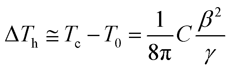 | (1) |
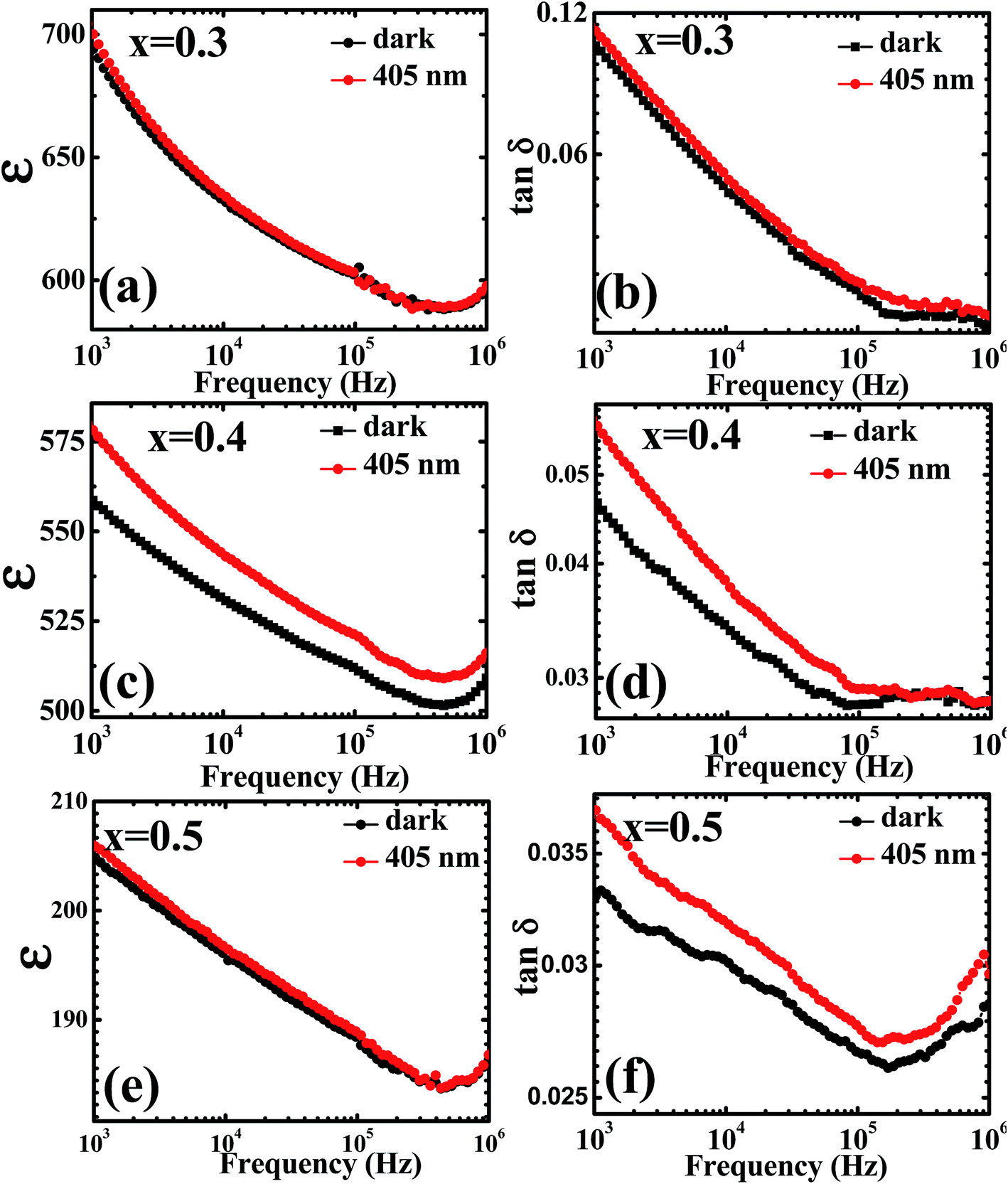 | ||
| Fig. 4 Room temperature dielectric constant and loss tangent measured for PLBZT in the frequency range of 1 kHz to 1 MHz under dark and illuminated condition of LASER for x = 0.3 (a and b), 0.4 (c and d), 0.5 (e and f). | ||
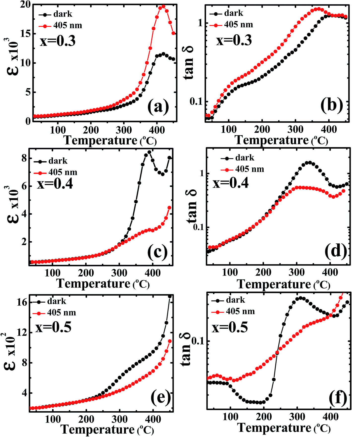 | ||
| Fig. 5 Dependence on temperature of dielectric constant and loss of PLBZT under dark and illumination of coherent source of LASER 405 nm x = 0.3 (a and b), 0.4 (c and d), 0.5 (e and f) at frequency of 5 kHz in the temperature range of 25–450 °C. | ||
A comparative study of temperature dependent dielectric constant and loss tangent has been carried out on these compositions under dark and illumination of light conditions at 5 kHz probe frequency over a wide range of temperatures (from 25–450 °C) as shown in Fig. 5(a)–(f). The enhancement in dielectric constant was observed for composition x = 0.3, but the magnitude of dielectric constant suppressed for x = 0.4 and 0.5 under illumination conditions near the phase transition temperature. The change in the magnitude of dielectric constant and Curie points can be understood in context of recharging of photo-active trap centers of charge carriers. The equation determines the change in Curie points under illumination is as follows: 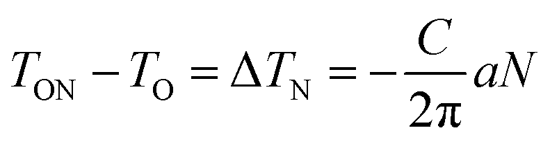 where, TON is Curie point in presence of charge carriers (N) under illumination, TO is Curie point in absence of light assisted charge carriers, C is Curie constant, and
  is a constant obtained by minimizing the free energy.35 The enhancement/decrease in the magnitude of dielectric constant near Curie temperature may be also ascribed to other causes, namely, an intrinsically high polarizability near Curie points due to their ionic displacement or alternatively, morphology features at the interface of the grains/grain boundaries, and with the interface of transparent electrode/electrolytes that modified the polarizability and hence total dielectric properties. The thermodynamics of ferroelectric ceramics indicates that an opto-dielectric phenomenon is not fully understood based on their microscopic and macroscopic phase transition mechanisms. It is also possible that during ferroelectric phase transition under illumination, large number of photo-generated charge carriers significantly affect the unit cell volume.53 The effective dielectric constant has dependence on the presence and concentration of photo generated charge carriers. Note that one can include the extrinsic effects such as Maxwell–Wagner space charge effects, but tangent loss also follows the same behavior, i.e. it significantly decreases near the phase transition temperature under illumination.
(e) Room temperature photo-ferroelectricity, displacement current and PUND analysis
Polarization was measured for PLBZT for x = 0.3, 0.4 and 0.5 on poled electro-ceramics. Fig. 6(a)–(c) show ferroelectric loops measured for 2 Hz under dark, illumination of a white light source, and monochromatic laser light, since bulk electro-ceramics do not respond to higher probe frequency.54 Correspondingly derived displacement currents are shown in Fig. 6(d)–(f) for the same conditions. A well defined peak in displacement current can be seen for x = 0.3 & 0.4 which increases under illumination of light; however, for higher compositions it shows only a sharp edge of resistive switching. Under illumination conditions non-equilibrium charge carriers appear which change the electron density and favor the overall enhancement in polarization. The mechanism is associated with the screening of ferroelectric polarization by the charge localized at the levels in the volume and on the surface. This mechanism causes bending of the bands and results in an internal field distribution.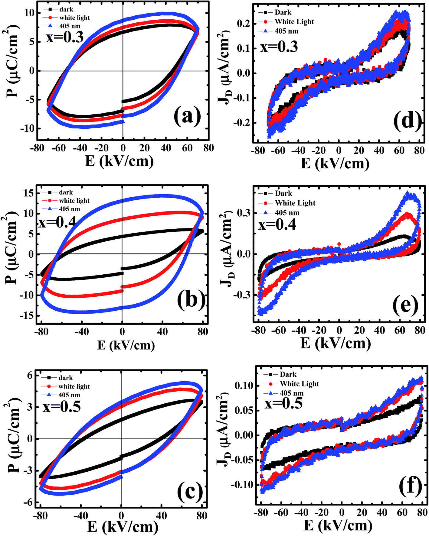 | ||
| Fig. 6 Ferroelectric polarization measured under three different condition i.e. dark, white light source and monochromatic laser having 405 nm wavelength for x = 0.3 (a), 0.4 (b), 0.5 (c). Switching of displacement current derived from ferroelectric polarization loop for x = 0.3 (d), 0.4 (e), 0.5 (f). | ||
On switching of E-field (electric field) in the light, when the external field reverses its direction, the field strength in the illuminated sections increases, especially near the surface where the screening charge is localized. Non-equilibrium carriers, which redistribute under E-fields applied to the ceramics, influence the overall polarization (electronic: due to change in spectral weight; and ionic: ionic displacement of cations at A- and B-site). We understand that under the influence of white or of monochromatic light the optically active materials absorb photon energy to fill the traps, shift the spectral weight of electronic orbitals, and hence influence the polarization.55–57 The enhancement in polarization by the photo-induced charge carriers can be attributed towards the compensation of depolarization field.
Under exposure of white light source the observed polarization (Pr) increased 50–150%, which may be due to the compensation of the internal depolarization field by photo-induced charge carriers, electronic polarization and ionic shift in various A- and B-site cations.8 The polarization also increased by 100–250% under 405 nm monochromatic laser light compared to dark polarization, it may be due to energy matching of laser light to that of bandgap of materials. These results suggest anomalous enhancement in spontaneous and remnant polarizations under illumination and may be a suitable candidate for devices working on the principle of the switching of displacement currents.
Here we also determine logic characteristics of the PLBZT ceramics using PUND (Positive Up and Negative Down) measurement for ferroelectric memory elements based on a series of five pulses. Fig. 7 shows that PUND measurements were performed at 80 kV cm−1 E-field stress and pulse width at 100 ms time. The calculation of the switchable polarization as follows: dP = P* − P∧ = where P* = (switchable polarization + non-switchable polarization) and P^ = (non-switchable polarization); 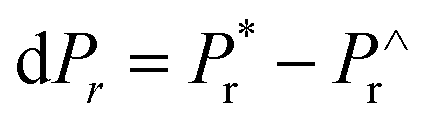 where
where  = (switchable remanent polarization + non-switchable remanent polarization) and
  = (non-switchable remanent polarization); theoretically the values of dP and dPr (experimental values in Table 3) in the same range. PUND analysis indicates almost 50–100% switchable polarization under illuminated conditions for x = 0.3, 0.4, 0.5, however among these three systems, x = 0.4 shows the highest switching under illumination. These results suggest that light illumination not only switches the polarization but also dictates the charge carriers.
 | ||
| Fig. 7 PUND characteristics for poled ceramics at applied E-field 80 kV cm−1 and pulse width 100 ms under dark and illuminated conditions for (a) x = 0.3, (b) x = 0.4, (c) x = 0.5. | ||
| Conditions | Compositions | ||||||||
|---|---|---|---|---|---|---|---|---|---|
| x = 0.3 | x = 0.4 | x = 0.5 | |||||||
| Dark | White light | Laser | Dark | White light | Laser | Dark | White light | Laser | |
| dP (μC cm−2) | 13.55 | 15.47 | 17.12 | 14.79 | 21.35 | 28.27 | 36.26 | 38.13 | 44.05 |
| dPr (μC cm−2) | 13.87 | 15.48 | 17.47 | 14.97 | 21.71 | 28.37 | 36.11 | 37.96 | 44.15 |
(f) Current conduction mechanisms
Current density (J) versus electric field (E) measurement data in dark and under white light source is shown in Fig. 8(a)–(c). Symmetrical leakage current behaviors were observed for series of compositions x = 0.3 to 0.5 up to ±60 kV cm−1 E-field stress. A kink in the conduction data near 45 kV cm−1 to 55 kV cm−1 was seen that represents the displacement current switching near the coercive fields. Inset data show leakage current behavior of unpoled electro-ceramics for their respective compositions. After E-poling, nearly saturated and trap-free charge carriers were present in the matrix that also significantly (at least an order) increased under illumination. These results suggest the development of surface charge carriers near electrode–electrolyte interface and hopping of trapped charges across grain boundaries to the nearest neighbor positions under illumination of light. | ||
| Fig. 8 Leakage current density (J) as function of electric field (E) for PLBZT systems for poled electroceramics (inset unpoled) under dark and illumination of white light source: (a) x = 0.3, (b) x = 0.4, (c) x = 0.5. Conduction mechanisms for PLBZT ceramics studies using J–E characteristics SCLC process for electrically poled electroceramics and fitted with SCLC (log(J) vs. log(E)) plots for (d) x = 0.3, (e) x = 0.4, (f) x = 0.5. | ||
In the hope of understanding the mechanism responsible for conduction for PLBZT ceramics, we have considered four main mechanisms, space charge limited conduction (SCLC) mechanisms,58 Schottky emission (SE),59 modified Schottky–Simmons model,60 and bulk-limited Poole–Frenkel (PF).61 These models are commonly used to describe carrier transport in ceramics/ferroelectrics. We fitted J–E data for quantitative analysis of charge transport in matrix and across interface. Depending on the type of charge transport, experimental data should satisfy straight line fits, and the optical dielectric constant of materials can be extracted theoretically from the magnitude of slopes. Therefore we present some set of results analyzed in terms of the different models.
First we have fitted our data for SCLC conduction mechanism where charge carriers are dominated by space charge (either from free or trapped carriers). The current density (J) is expected to have a power-law dependence on applied E-field (J ∝ En).62
 | (2) |
Fig. 8(d)–(f) show the linear fitting of logJ vs. logE, it provides slopes for x = 0.3, 0.4, 0.5 under dark and illuminated conditions for poled ceramics. It can be easily identified two distinct regions, one below coercive fields and above coercive fields. The linear dependence of logJ–logE plot in both regions satisfy the power-law dependence. Below coercive fields, the values of exponents (n) were found to be in the range of 1.29 to 2, which is compatible with the discrete trap assisted conduction mechanisms. Therefore we believe that trap assisted discrete conduction mechanisms may be one of the dominant factors to control the conduction process in PLBZT ceramics in both conditions. These findings suggest that optically active Li/Bi cations at A-site can redistribute the anion (oxygen) vacancies and defects trapped across grains and grain boundaries.
The optical dielectric constants obtained from the slopes of graphs lnJ vs. E1/2 (pure Schottky model, Fig. 9(a)–(c)) are in the range of 0.3 to 1.9 for x = 0.3 and 0.4 which provide unrealistic values of optical dielectric constant hence ruled out its importance. Later we have fitted our data for Schottky–Simmons model and Poole–Frenkel (βPF = 2β) for the determination of optical dielectric constant as shown in Fig. 9(d)–(f) for Schottky–Simmons/Poole–Frenkel model. The observed data linearly fit the Schottky–Simmons/Poole–Frenkel models (most suitable for oxides where charge carriers possess short mean-free paths and bulk process), however, the experimental data for optical dielectric constant of Ti rich PZT only matched with the Poole–Frenkel model with (ξ = 1 and βPF = 2β), similar results were obtained for thick PZT thin films by Zubko et al. The detail values of optical dielectric constants obtained for Poole–Frenkel model/Schottky–Simmons model are given in the Table 4. One can correctly distinguish between the Poole–Frenkel (PF) (ξ is nearly 1) model and Schottky–Simmons model (ξ is nearly 2) based on the thickness dependent I–V data and variation of constant ξ from 1 to 2. It can be easily seen from the Table 4 that with increase in ξ values, the optical dielectric constant values obtained from the slopes of various experimental data deviate from the optical dielectric constant (∼6–8) of Ti rich PZT reported in literature,63 hence ruled out the Schottky–Simmons model (interface limited) and support PF mechanisms (bulk conduction). However, the optical dielectric constant obtained from the slopes for x = 0.5 compositions favor either Schottky–Simmons model or discrete trap assisted SCLC mechanism. At least for x = 0.5 samples require further thickness dependent study to reach any further conclusion which is beyond the scope of present investigation.
 | ||
| Fig. 9 Leakage current density (J) as function of electric field (E) fitted with Schottky emission (a) x = 0.3, (b) x = 0.4, (c) x = 0.5 and fitted with modified Schottky–Simmons equation/Poole–Frenkel model (d) x = 0.3, (e) x = 0.4, (f) x = 0.5 under dark and illumination of white light. | ||
| Conditions | (ξ, K, & slopes) | |||||
|---|---|---|---|---|---|---|
| Poole–Frenkel model valid for ξ = 1 (x = 0.3) | Poole–Frenkel model valid for ξ = 1 (x = 0.4) | Poole–Frenkel model valid for ξ = 1 (x = 0.5) | ||||
| Dark | White light | Dark | White light | Dark | White light | |
| Values of slopes | 0.01245 | 0.0108 | 0.0105 | 0.0093 | 0.0039 | 0.0066 |
| K (ξ = 1) | 5.6 | 7.4 | 7.8 | 9.9 | 52 | 19.7 |
| K (ξ = 1.25) | 3.5 | 4.7 | 5.0 | 6.3 | 36 | 12 |
| K (ξ = 1.5) | 2.4 | 3.2 | 3.4 | 4.4 | 25 | 8.7 |
| K (ξ = 1.75) | 1.8 | 2.4 | 2.5 | 3.2 | 18 | 6.5 |
| K (ξ = 2) | 1.3 | 1.8 | 1.9 | 2.4 | 14 | 4.5 |
Schottky emission model:
 | (3) |
Schottky–Simmons model:
 | (4) |
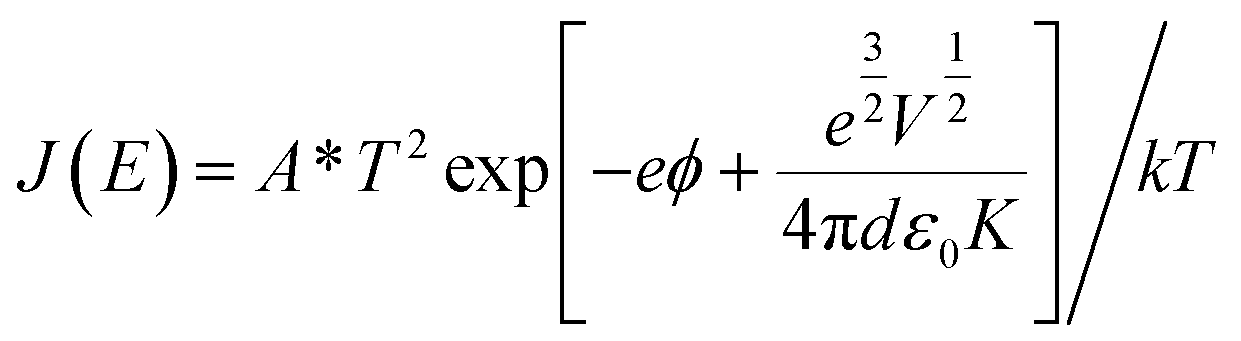
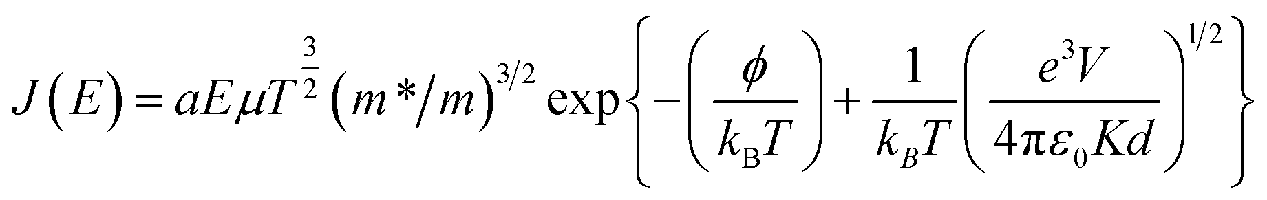
Poole–Frenkel model/Schottky–Simmons model:
 | (5) |
 , α = 3 × 10⁻⁴ A s cm−3 K−3/2, J is current density, V is applied voltage, μ is carrier mobility, m* and m are the effective and free electron mass, respectively, ε0 is permittivity in free space, k is Boltzmann constant, T is absolute temperature, K is optical dielectric constant, and ϕ is barrier height. For Poole–Frenkel model: βPF = 2β and ξ is nearly 1 to 1.25 and for Schottky–Simmons model ξ is near to 1.75 to 2, depending on the microstructure and materials internal properties.
The current conduction mechanisms also depend on the work function of electrodes and their conductivity. We have used a transparent electrode ITO (50 ohm) as top electrode to check the leakage current under the illumination of light. The energy band diagram of ITO/PLBZT/Ag structure suggests well defined Schottky barrier height. The work function of ITO is 4.7 eV, PLBZT is (electron affinity (3.5 eV) + bandgap (3.2–3.4 eV)), and bottom electrode Ag is 4.8 eV. Illumination of light modifies the Fermi energy and populates the conduction band hence effectively reduce the Schottky barrier height and hence effectively increase the charge injection across electrode–dielectric interface. The modification of barrier height and development of space-charge in matrix together influence the leakage current under dark and illumination conditions.21
The optically active charge carriers remarkably changed the spectral weight of electrons, improve their hybridization, and allow scattering of activated charge carriers at Li/Bi cations. The photo-generated charge carriers are rather uniformly distributed in the samples; even in the case of reversed polarity, illumination enhanced conductivity at least an order of magnitude. This study also highlights the evidence for long lasting generation of photo charge carries and their strong photon–phonon–electron coupling. It is evident that considerable amount of photo-carriers generate under illumination of white light near to the top electrode of a materials which drift towards other electrode via grains and grain boundaries (bulk limited) under external biased E-field, during the course of transportation, these carriers fill the traps, compensate the charge carriers across the grains and grain boundaries interface.
4. Conclusions
An optically active family of opto-ferroelectrics (PLBZT for x = 0.3, 0.4, 0.5) has been successfully discovered which shows giant polarization switching under illumination of light. These systems possess tetragonal crystal structure with P4mm space group symmetry with increase in in-plane lattice constant (a) and decrease in out of plane lattice constant (c) with increase in Li/Bi substitution. The systems with x = 0.4 & 0.5 show almost 10–15 °C shift in Curie points towards lower temperature and a significant reduction in the magnitude of dielectric constant under illumination near the ferroelectric phase transition temperature. Interestingly illumination of light also reduced the tangent lost at room temperature and near Curie points, these observations ruled out the possible role of Maxwell–Wagner effects on dielectric and polarization properties. The polarization and related displacement currents significantly switched under illumination of light depending on the probed frequencies and applied E-fields. The current conduction mainly obeys bulk limited Poole–Frenkel mechanism which provides the optical dielectric constant similar to Ti-rich PZT. The illumination of light changes the spectral weight of electronic orbitals, reorient the polarization, and strengthens the ionic polarization vector in direction applied E-fields resulting a giant switching of polarization under illumination. Hopefully these results guide the ferroelectric family to develop new optically active ferroelectrics for possible uses as electrically WRITE and optically READ non-volatile memory elements, ferro-photovoltaic materials and holographic imaging.Acknowledgements
Hitesh Borkar would like to acknowledge the UGC (SRF, Grant No. F.2-61/98 (SA-I)) to provide fellowship to carry out Ph.D. program. Authors would like to thank Prof. R. S. Katiyar (University of Puerto Rico, USA) for XPS measurements and Dr B. P. Singh for Raman experiment. Authors sincerely thank the Director, NPL New Delhi, Dr Ranjana Mehrotra and Dr Sanjay Yadav for their constant encouragement.References
- V. M. Fridkin, Photoferroelectrics, Springer-Verlag, Berlin, 1979 Search PubMed.
- V. K. Wadhawan, Introduction to Ferroic Materials, Gordon and Breach Science Publishers, Amsterdam, 2000 Search PubMed.
- S. Y. Yang, J. Seidel, S. J. Byrnes, P. Shafer, C. H. Yang, M. D. Rossell, P. Yu, Y. H. Chu, J. F. Scott, J. W. Ager, L. W. Martin and R. Ramesh, Nat. Nanotechnol., 2010, 5, 143–147 CrossRef CAS PubMed.
- R. Blinc, G. Tavčar, B. Žemva, D. Hanžel, P. Cevc, C. Filipič, A. Levstik, Z. Jagličić, Z. Trontelj, N. Dalal, V. Ramachandran, S. Nellutla and J. F. Scott, J. Appl. Phys., 2008, 103, 074114 CrossRef.
- R. Blinc, B. Zalar, P. Cevc, A. Gregorovič, B. Žemva, G. Tavčar, V. Laguta and J. F. Scott, J. Phys.: Condens. Matter, 2009, 21, 045902–045904 CrossRef CAS PubMed.
- R. Blinc, G. Tavčar, B. Žemva, E. Goreshnik, D. Hanžel, P. Cevc, A. Potočnik, V. Laguta, Z. Trontelj, Z. Jagličič and J. F. Scott, J. Appl. Phys., 2009, 106, 023924 CrossRef.
- K. Yamauchi and S. Picozzi, Phys. Rev. Lett., 2010, 105, 107202–107204 CrossRef PubMed.
- A. L. Kholkin, S. O. Iakovlev and J. L. Baptista, Appl. Phys. Lett., 2001, 79, 2055–2057 CrossRef CAS.
- A. Bokov and Z. G. Ye, J. Mater. Sci., 2006, 41, 31–52 CrossRef CAS.
- W. Zhong and D. Vanderbilt, Phys. Rev. Lett., 1995, 74, 2587–2590 CrossRef CAS PubMed.
- L. M. Belyaev, I. I. Groshik, V. V. Lyakhovitskaya, V. N. Nosov and V. M. Fridkin, JETP Lett., 1967, 6, 16–17 Search PubMed.
- B. I. Sturman and V. M. Fridkin, in The Photovoltaic and Photorefractive Effects in Noncentrosymmetric Materials, Ferroelectricity and Related Phenomena, ed. G. W.Taylor, Gordon and Breach, New York, 1992, vol. 8. Search PubMed.
- M. Dawber, Physics, 2012, 5, 63–66 CrossRef.
- G. Giovannetti and J. V. D. Brink, Phys. Rev. Lett., 2008, 100, 227603–227604 CrossRef PubMed.
- K. Kobayashi, S. Horiuchi, R. Kumai, F. Kagawa, Y. Murakami and Y. Tokura, Phys. Rev. Lett., 2012, 108, 237601–237605 CrossRef PubMed.
- C. Alemany, L. Pardo, B. Jimenez, F. Carmona, J. Mendiola and A. M. Gonzalez, J. Phys. D: Appl. Phys., 1999, 32(17), L79 CrossRef CAS.
- M. L. Calzada, R. Jimenez, A. Gonzalez, J. Garcıa-Lopez, D. Leinen and E. Rodrıguez-Castellon, Chem. Mater., 2005, 17(6), 1441 CrossRef CAS.
- V. M. Fridkin and R. M. Magomadov, Pis'ma Zh. Eksp. Teor. Fiz., 1979, 30, 723–726 CAS.
- T. Choi, S. Lee, Y. J. Choi, V. Kiryukin and S. W. Cheong, Science, 2009, 324, 63–65 CrossRef CAS PubMed.
- R. Nechache, C. Harnagea, S. Li, L. Cardenas, W. Huang, J. Chakrabartty and F. Rosei, Nat. Photonics, 2015, 9, 61 CrossRef CAS.
- X. Z. Zhai, H. M. Deng, W. L. Zhou, P. X. Yang, J. H. Chu and Z. Zheng, RSC Adv., 2015, 5, 82351 RSC.
- J. Wang, J. B. Neaton, H. Zheng, V. Nagarajan, S. B. Ogale, B. Liu, D. Viehland, V. Vaithyanathan, D. G. Schlom, U. V. Waghmare, N. A. Spaldin, K. M. Rabe, M. Wuttig and R. Ramesh, Science, 2003, 299, 1719–1722 CrossRef CAS PubMed.
- J. Wang, C. S. Sandu, E. Colla, Y. Wang, W. Ma, R. Gysel, H. J. Trodahl and N. Setter, Appl. Phys. Lett., 2007, 90, 133107–133113 CrossRef.
- S. R. Basu, L. W. Martin, Y. H. Chu, M. Gajek, R. Ramesh, R. C. Rai, X. Xu and J. L. Musfeldt, Appl. Phys. Lett., 2008, 92, 091905–091913 CrossRef.
- A. J. Hauser, J. Zhang, L. Mier, R. A. Ricciardo, P. M. Woodward, T. L. Gustafson, L. J. Brillson and F. Y. Yang, Appl. Phys. Lett., 2008, 92, 222901–222903 CrossRef.
- G. Arlt, H. Dederichs and R. Herbiet, Ferroelectrics, 1987, 74, 37–53 CrossRef CAS.
- G. Luchaninov, A. V. Shilinkov, L. A. Shavalov and I. J. Shipkova, Ferroelectrics, 1989, 98, 123–126 CrossRef.
- C. A. P. Araujo, J. D. Cuchiare, L. D. McMillan, M. C. Scott and J. F. Scott, Nature, 1995, 374, 627–629 CrossRef.
- Z. G. Zhu, B. S. Li, G. R. Li, W. Z. Zhang and Q. R. Yin, Mater. Sci. Eng., B, 2005, 117, 216 CrossRef.
- P. W. M. Blom, R. M. Wolf, J. F. M. Cillessen and M. Krijn, Phys. Rev. Lett., 1994, 73, 2107–2110 CrossRef CAS PubMed.
- L. Pintilie, I. Boerasu, M. J. M. Gomes, T. Zhao, R. Ramesh and M. Alexe, J. Appl. Phys., 2005, 98, 124104–124109 CrossRef.
- L. Pintilie and M. Alexe, J. Appl. Phys., 2005, 98, 124103–124108 CrossRef.
- H. Borkar, M. Tomar, V. Gupta, J. F. Scott and A. Kumar, Appl. Phys. Lett., 2015, 107(12), 122904–122905 CrossRef.
- B. Noheda, J. A. Gonzalo, R. Guo, S. E. Park, L. E. Cross, D. E. Cox and G. Shirane, Phys. Rev. B: Condens. Matter Mater. Phys., 2000, 61, 8687–8695 CrossRef CAS.
- J. Rouquette, J. Haines, V. Bornand, M. Pintard, P. Papet and J. L. Sauvajol, Phys. Rev. B: Condens. Matter Mater. Phys., 2006, 73, 224118–224125 CrossRef.
- J. F. Meng, R. S. Katiyar, G. T. Zou and X. N. Wang, Phys. Status Solidi A, 1997, 164, 851–862 CrossRef CAS.
- R. S. Katiyar, J. F. Ryan and J. F. Scott, Phys. Rev. B: Solid State, 1971, 4, 2635–2638 CrossRef.
- G. Burns and B. A. Scott, Phys. Rev. B: Condens. Matter Mater. Phys., 1973, 7, 3088 CrossRef CAS.
- A. Kumar, N. M. Murari and R. S. Katiyar, Appl. Phys. Lett., 2007, 90, 262907 CrossRef.
- C. M. Foster, Z. Li, M. Grimsditch, S. K. Chan and D. J. Lam, Phys. Rev. B: Condens. Matter Mater. Phys., 1993, 48, 10160–10167 CrossRef CAS.
- T. Ostapchuk, J. Petzelt, V. Zelezny, S. Kamba, V. Bovtun, V. Porokhonskyy, A. Pashkin, P. Kuzel, M. D. Glinchuk, I. P. Bykov, B. Gorshunov and M. Dressel, J. Phys.: Condens. Matter, 2001, 13, 2677–2689 CrossRef CAS.
- L. E. Mcneil, M. Grimsditch and R. H. French, J. Am. Ceram. Soc., 1993, 76, 1132–1136 CrossRef CAS.
- A. Kumar, N. M. Murari and R. S. Katiyar, Appl. Phys. Lett., 2008, 92(15), 152907–152913 CrossRef.
- A. Slodczyk, P. Colomban and M. Pham-Thi, J. Phys. Chem. Solids, 2008, 69, 2503–2513 CrossRef CAS.
- M. P. Thi, G. March and P. Colomban, J. Eur. Ceram. Soc., 2005, 25, 3335–3346 CrossRef CAS.
- L. E. Stoflea, N. G. Apostol, L. Trupin and C. M. Teodorescu, J. Mater. Chem. A, 2014, 2, 14386 CAS.
- K. W. Schroder, H. Celio, L. J. Webb and K. J. Stevenson, J. Phys. Chem. C, 2012, 116, 19737–19747 CAS.
- S. U. Awan, S. K. Hasanain, M. F. Bertino and G. H. Jaffari, J. Phys.: Condens. Matter, 2013, 25, 156005 CrossRef PubMed.
- M. K. Kuneva and V. I. Krastev, J. Mater. Sci.: Mater. Electron., 2000, 11, 629 CrossRef CAS.
- H. Borkar, V. Rao, S. Dutta, A. Barvat, P. Pal, M. Tomar, V. Gupta, J. F. Scott and A. Kumar, J. Phys.: Condens. Matter, 2016, 28, 265901 CrossRef PubMed.
- M. Nagoshi, T. Suzuki, Y. Fukuda, K. Ueki, A. Tokiwa, M. Kiruchi, Y. Syono and M. Tachiki, J. Phys.: Condens. Matter, 1992, 4, 5769–5781 CrossRef CAS.
- A. Kumar, D. Barrionuevo, N. Ortega, A. K. Shukla, S. Shannigrahi, J. F. Scott and R. S. Katiyar, Appl. Phys. Lett., 2015, 106(13), 132901 CrossRef.
- K. T. Butler, J. M. Frost and A. Walsh, Energy Environ. Sci., 2015, 8, 838–848 CAS.
- J. F. Scott, J. Phys.: Condens. Matter, 2008, 20, 021001–021002 CrossRef.
- L. Pintilie, I. Vrejoiu, G. Le Rhun and M. Alexe, J. Appl. Phys., 2007, 101, 064109–064118 CrossRef.
- J. Robertson, W. L. Warren and B. A. Tuttle, J. Appl. Phys., 1995, 77, 3975–3980 CrossRef CAS.
- D. Dimos, W. L. Warren, M. B. Sinclair, B. A. Tuttle and R. W. Schwartz, J. Appl. Phys., 1994, 76, 4305–4315 CrossRef CAS.
- B. Nagaraj, S. Aggarwal, T. K. Song, T. Sawhney and R. Ramesh, Phys. Rev. B: Condens. Matter Mater. Phys., 1999, 59, 16022–16027 CrossRef CAS.
- S. M. Sze, Physics of Semiconductor Devices, Wiley, New York, 2nd edn, 1981 Search PubMed.
- J. G. Simmons, J. Appl. Phys., 1964, 35, 2472–2481 CrossRef.
- P. Zubko, D. J. Jung and J. F. Scott, J. Appl. Phys., 2006, 100, 114113–114117 CrossRef.
- R. H. Tredgold, Space Charge Conduction in Solids, Elsevier Publishing Company, Amsterdam, 1966 Search PubMed.
- (a) Z. Huang, X. Meng, P. Yang, Z. Zhang and J. Chu, Appl. Phys. Lett., 2000, 76, 3980–3982 CrossRef CAS; (b) J. Robertson and C. W. Chen, Appl. Phys. Lett., 1999, 74, 1168–1170 CrossRef CAS.
| This journal is © The Royal Society of Chemistry 2017 |