
 Open Access Article
 This Open Access Article is licensed under a
 Creative Commons Attribution 3.0 Unported Licence
Facile synthesis of various epitaxial and textured polymorphs of vanadium oxide thin films on the (0006)-surface of sapphire substrates†
Bin Honga,
Jiangtao Zhaoa,
Kai Hua,
Yuanjun Yang *abd,
Zhenlin Luoab,
Xiaoguang Lic and
Chen Gao*ab
*abd,
Zhenlin Luoab,
Xiaoguang Lic and
Chen Gao*ab
aNational Synchrotron Radiation Laboratory, Collaborative Innovation Center of Chemistry for Energy Materials, University of Science and Technology of China, Hefei, Anhui 230029, P. R. China. E-mail: yangyuanjun@ustc.edu.cn; cgao@ustc.edu.cn
bCAS Key Laboratory of Materials for Energy Conversion, Department of Materials Science and Engineering, University of Science and Technology of China, Hefei, Anhui 230026, P. R. China
cDepartment of Physics and Hefei National Laboratory for Physical Sciences at Microscale, University of Science and Technology of China, Hefei, Anhui 230027, P. R. China
dSchool of Electronic Science and Applied Physics, Lab of Quantum Materials and Interfaces, Hefei University of Technology, Hefei, Anhui 230009, P. R. China
First published on 21st April 2017
Abstract
Extensive attention has been paid to vanadium oxide polymorphs because of their potential to be used in applications in information and optoelectronic devices, as well as in energy harvesting technologies. However, vanadium oxides always form a very complex phase diagram; in particular, it is still challenging to synthesize pure vanadium oxide epitaxial polymorphs on low-cost, transparent and wafer-scale substrates. Here, we demonstrate the growth of epitaxial polymorphs of vanadium oxide (VO2 (R, M1 and their mixed phase), and V2O3) and (001)-textured VO2 (B) thin films on the (0006) surface of sapphire without selecting specific substrate orientations. This is achieved by controlling the vanadium arrival rate via sputtering power and oxidation of vanadium atoms through the partial pressure of oxygen using magnetron sputtering techniques, which enables wafer-scale production of the vanadium oxide thin films on the sapphire substrates. Growth phase diagrams of the various polymorphs are also developed for guiding device design based on the vanadium oxide thin films. This work paves a way towards practical applications of vanadium oxide thin films on chemically stable, transparent and low-cost sapphire substrates.
1. Introduction
Transition metal oxides (TMOs) have attracted increasing research interest around the world1–3 owing to their wide range of practical applications such as in field-effect transistors,4 optoelectronic devices,5 and memory devices.6 It is well known that TMOs always exhibit various polymorphic structures (e.g. multiferroic BiFeO3 thin films with tetragonal, rhombohedral, and monoclinic phases7) and are closely related to each other in a thermodynamic framework, which can lead to difficulties during synthesis, especially for thin film forms.8,9 Analogous vanadium oxide is indeed one of the most complicated of the TMOs; it can exhibit various oxidation states (such as V2+, V3+, V4+, or V5+) and various crystal structures even with the same oxidation states.10–12 For instance, vanadium dioxide (VO2) has six or more polymorphs (e.g., R, M1, M2, A, B, C) with the same chemical formula.Among these phases, monoclinic VO2 (M1) is the most widely studied owing to its abrupt metal–insulator transition (MIT) at around 68 °C, coupled with a structural transition from a low-temperature monoclinic (M1 phase) to a high-temperature rutile (R phase) structure.13,14 The VO2 (M2 phase) polymorph is often observed as a metastable phase in the vicinity of the metal–insulator transition (MIT) of the VO2 (M1) nanowires and nanobeams.11,15,16 VO2 (A) is another metastable octahedrally coordinated phase composed of edge and corner-sharing VO6 octahedra. The phase transition behavior is quite different from the M1 and R phase. VO2 (A) is transformed to the R phase, but this change is not reversible by changing the temperature.17 VO2 (B) is also a metastable compound; it can be converted to a rutile or monoclinic structure after a suitable annealing process.8,18 Further, it is a promising material for energy applications, as it can be used as an electrode in Li-ion batteries.19,20 Meanwhile, VO2 (C) consists of layers of square VO5 pyramids, each of which shares its four basal edges with four neighboring square VO5 pyramids.21 The formation of these mixed and similar phases very often hinders the accurate understanding of the physical properties of the vanadium oxide polymorphs. Moreover, preparation of pure phases and high-quality crystalline thin films has been a major challenge for vanadium oxide thin films and related device applications. An increasing number of studies on vanadium oxide have focused on epitaxial thin films, which can be grown using a variety of deposition techniques.3,9,22–25 However, it is difficult to prepare pure vanadium oxides, especially thin films, of high crystalline quality because of the narrow range of the phase diagram, complex oxidation states of vanadium, and species diversity of the polymorphs (as mentioned above, there are at least six phases of VO2). Recently, Ho Nyung Lee and coworkers8 selectively grew tetragonal VO2 (A) on (011)-oriented SrTiO3 (STO) and LaAlO3 substrates, monoclinic VO2 (B) on a wide range of (001)-oriented perovskite substrates, and monoclinic VO2 (M1) on (111)-oriented STO, (LaAlO3)0.3(SrAl0.5Ta0.5O3)0.7 and LaAlO3 substrates using pulsed laser epitaxy. They also successfully grew epitaxial vanadium dioxide films of phase A, B, and M1 on (011), (001), and (111)-oriented STO substrates, respectively.26 Furthermore, T. Venkatesan et al.27 grew high-quality single epitaxial films of tetragonal VO2 (A), monoclinic VO2 (B), and VO2 (M1) thin films on (100)-oriented STO substrates using pulsed laser deposition.
Despite some recent progress in preparing vanadium oxide thin films, accessing vanadium oxide polymorphs generally depends upon using expensive substrates and carefully selecting different crystallographic orientations for different phases. In this work, we have successfully fabricated epitaxial thin films of vanadium sesquioxide (V2O3) and various dioxide polymorphs (VO2 (R), VO2 (M1), and VO2 (B)) on single cut (0006) sapphire surfaces using reactive ion magnetron sputtering. This technique enables wafer-scale production of vanadium oxide thin films. Moreover, the sapphire substrate (Al2O3 crystal, normally several inches in size) is much cheaper than substrates such as STO or LAST. In addition, the sapphire substrate is so transparent in ultraviolet, visible and infrared regions that it can be used to design optoelectronic devices based on the vanadium oxide thin films.
2. Experimental
A vanadium metal disk in 2-in size was used as the sputtering target. The detailed growth conditions were presented and discussed in the main text. X-ray diffraction (XRD) was performed on Smartlab (Riguka, Japan) and partially on the 14B endstation in Shanghai synchrotron radiation facilities (SSRF). X-ray absorption spectroscopy (XAS) measurements were performed on the 08U in SSRF. We used inVia Raman microscope (Renishaw) to collect Raman spectra with a 532 nm laser. All the above measurements were finished at room temperature. The electrical transports were measured by physical property measurement system (Quantum Design).3. Results and discussion
Fig. 1(a)–(d) shows the crystal structures with different symmetries of several typical vanadium oxides of VO2 (R), VO2 (B) VO2 (M1) and V2O3. To confirm the crystalline phases of the fabricated vanadium oxide thin films, X-ray diffraction (XRD) measurements were performed using a diffractometer equipped with a Ge (220) × 2 monochromator at a wavelength of 1.5406 Å. As shown in upper inset of Fig. 1(e), the characteristic (200) peak of the VO2 thin films occurs at about 39.5° by θ–2θ scans, which is the feature of tetragonal phase (rutile phase).28 The corresponding lattice constant a is determined to be ∼4.559 Å and the out-of-plane lattice distortion (abulk − afilm)/abulk is −0.11%. In the lower part of Fig. 1(e), the peak at 2θ = 39.85° is assigned to the (020) reflections of VO2 (M1). The series of the (001) reflections visible in Fig. 1(f) are assigned to the pure VO2 (B) phase. The interplane space in this VO2 (B) thin film is calculated to be ∼6.156 Å, which is in line with the previous reports.8 It is interesting that the mixed-phase VO2 (M1) and VO2 (mM, monoclinic metallic phase), and the mixed-phase VO2 (B) and VO2 (M1) were also fabricated as shown in the middle and lower part of Fig. 1(e) and (f). It's not hard to imagine that the interfaces between two different phases (e.g. VO2 M1 and B phases) in the mixed-phase VO2 system would modulate the MIT behaviors, which is very interesting and need to be further studied. Moreover, the peak at 2θ = 38.67° in the XRD pattern is assigned to the (0006) peak of the V2O3 phase in the upper inset of Fig. 1(f). The diffraction peaks from the sapphire substrates are marked by dotted cyan lines for comparisons in Fig. 1(e) and (f). Moreover, in order to check the purities and orientations of different crystalline phases, the full scans of vanadium oxide thin films are shown in Fig. S1 (please see ESI†). The above XRD analysis revealed that all vanadium oxide films with highly oriented growth habits are deposited on the single orientation on the (0006) sapphire substrates. Consequently, the desired and highly oriented vanadium oxide thin films can be grown on the single (0006) surface without changing the orientations of sapphire substrates through carefully controlling growth conditions.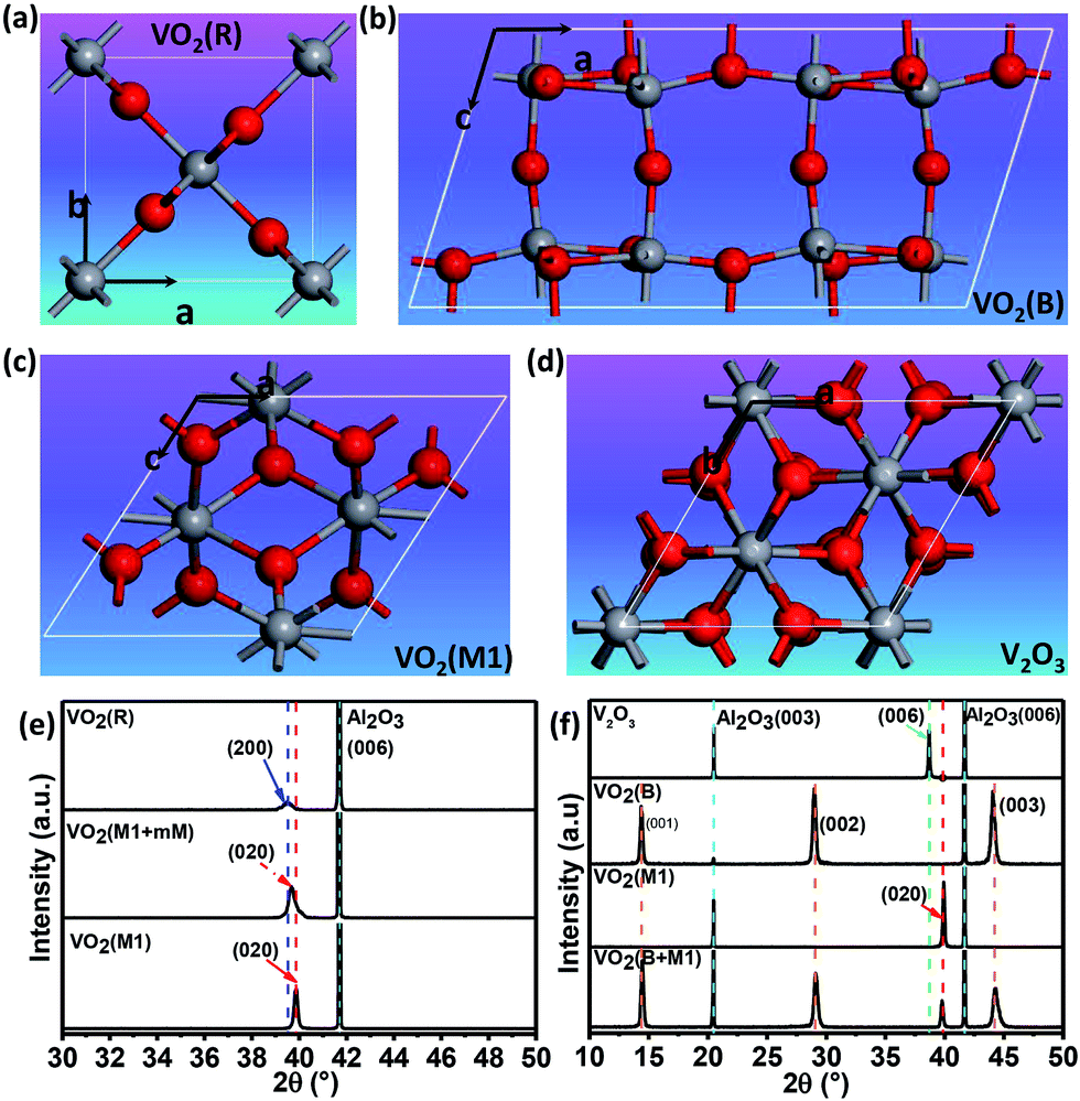 | ||
| Fig. 1 Schematic crystal structures of (a) rutile VO2 (R), (b) monoclinic VO2 (M1), (c) monoclinic VO2 (B), and (d) trigonal V2O3 phases. The red and gray spheres represent oxygen and vanadium atoms, respectively. (e) XRD patterns for VO2 (R), VO2 (M1 + mM), and VO2 (M1). (f) XRD patterns for V2O3 (R), VO2 (B), VO2 (M1), and the mixed-phase VO2 (B) and VO2 (M1). XRD pattern of VO2 (M1) is re-plotted here for better comparison among different epitaxial polymorphs. All the films were grown to ∼120 nm (ref. 44) by controlling deposition time (please see the ESI, Fig. S2†). The thicker films were chosen to minimize the substrate-induced strain effects. | ||
To clarify the epitaxial behaviors, XRD phi scans of the typical vanadium oxide thin films were also performed. Fig. 2(a) shows that V2O3 could be grown on the (006) sapphire with following epitaxy relationship: (001) V2O3//(006) Al2O3 and (100) V2O3//(100) Al2O3. Fig. 2(b) shows that (010) VO2 (M1)//(006) Al2O3 and (100) VO2 (M1)//(100) Al2O3. However, the VO2 (B) film (110) peaks are hardly observed by XRD phi scans as demonstrated in Fig. 2(c), which is also in the cases of the (−401), (020) and (113) peaks (not shown here). Therefore, the VO2 (B) thin film on the (0006) surface of sapphire favors the (001)-textured growth as similar as on the (001) surface of SrTiO3 substrate.29 This result is likely due to the in-plane random stacking of the 2-dimensional V–O layers.
 | ||
| Fig. 2 Phi scans of different vanadium oxide epitaxial thin films. (a) V2O3. (b) VO2 (M1), and (c) VO2 (B). (d) Raman spectra of different epitaxial polymorphs of VO2 and V2O3 thin films. The Raman peaks at around 417, 499, and 749 cm−1 (marked by the dashed red lines) are assigned to the Al2O3 substrate. | ||
In order to further confirm crystal structures of the above phases, Raman spectroscopy was utilized to study lattice dynamics and thus discriminate the these various vanadium oxide phases. The Raman spectra of several typical vanadium oxide at room temperature are shown in Fig. 2(d). Raman peaks at around 417, 499, and 749 cm−1 (marked by the dashed red lines) in Fig. 2(d) are assigned to the Al2O3 substrate. The Raman spectra of V2O3 exhibits prominent low-frequency modes at around 212, 230, and 294 cm−1 at room temperature, which is in agreement with results in previous studies.30 The three representative Raman peaks at around 193, 223, and 614 cm−1 correspond to the VO2 M1 phase, and the peak positions also agree well with literature values.31–34 However, no Raman peaks was observed in the metallic VO2 rutile phase and thus displays almost no Raman activity in line with the ref. 35. And the VO2 (B) thin film has the three typical vibrating modes at 159, 266 and 415 cm−1, which was also reported by Lee et al.8
Since the surface microstructures are very important for designing thin-film devices, the various vanadium dioxide polymorphs and V2O3 epitaxial thin films were investigated by atomic force microscopy (AFM). In topographical terms, both the VO2 (B + M1) and VO2 (B) films in Fig. 3(d) and (e) exhibit a larger grain size than the VO2 (R) and V2O3 films in Fig. 3(a) and (f). We noted that a relatively large proportion of the self-organized domain patterns separate out from the matrix of thin films in the VO2 (M1 + mM) phase (shown in Fig. 3(b)). Meanwhile, the pure VO2 (M1) in Fig. 4(c) shows that a continuous film is normally formed as reported in ref. 24 and 36.
 | ||
| Fig. 3 AFM images for the different V2O3 and VO2 epitaxial polymorphs on the (0006)-oriented sapphire substrates. | ||
 | ||
| Fig. 4 Phase diagram for different polymorphs of vanadium oxide thin films with growth temperature and oxygen flow (a), and RF power and oxygen flow (b). (c) The wafer scale production of VO2 epitaxial polymorphs in M1 phase. (d) Transport properties of different epitaxial polymorphs of VO2 and V2O3 epitaxial thin films. | ||
Based on the above characterizations, the vanadium oxide epitaxial polymorphs can be obtained as what one wants. By varying the power of the radio-frequency (RF) supply, argon and oxygen flow ratio, we could change the arrival rate of the atoms on the surface of the sapphire substrates. Moreover, by adjusting the oxygen flow rate and growth temperature, we could also change the oxidation of vanadium on the substrates. We found that the phase of the vanadium oxide thin films is more sensitive to the growth temperature with low oxygen flow levels (below 1.0 sccm, set argon flow of 50.6 sccm, and RF power of 60 W). We also found that the critical growth temperature is ∼490 °C. VO2 (R) was produced with low oxygen flow and at low temperature (oxygen flow < 1.0 sccm and temperature below 490 °C), while VO2 (M1) was produced above the critical temperature of ∼490 °C. Table 1 summarizes the crystal structure, lattice constants and optimized growth conditions for the pure VO2 (R), VO2 (M1), VO2 (B) phases and V2O3 on the (0006)-oriented sapphires, respectively.
| Vanadium oxide polymorphs | Crystal structure | Lattice constants in bulk | Growth condition | |||||
|---|---|---|---|---|---|---|---|---|
| a (Å) | b (Å) | c (Å) | β or γ (°) | Temp (°C) | Ar![[thin space (1/6-em)]](https://www.rsc.org/images/entities/char_2009.gif) :O2 (sccm) :O2 (sccm) |
Power (W) | ||
| VO2-R | P42/mnm | 4.554 | 4.554 | 2.855 | 90 | 400–480 | 50.6:(0.5–1.0) |
60 |
| VO2-M1 | P21/c | 5.752 | 4.526 | 5.382 | 122.6 | 400–500 | 50.6:(1.0–1.2) |
60 |
| 490 | 60.0:(1.0–2.8) |
80–120 | ||||||
| VO2-B | C2/m | 12.03 | 3.69 | 6.42 | 106.6 | 490 | 60.0:(1.0–3.0) |
50–80 |
| V2O3 | R![[3 with combining macron]](https://www.rsc.org/images/entities/char_0033_0304.gif) c c |
4.951 | 4.951 | 14.004 | γ = 120 | 490 | 60.0:<1.0 |
50–120 |
Consequently, we were able to construct a simple phase diagram for growing the different vanadium oxide polymorphs (shown in Fig. 2(a)) based on the effects of oxygen flow and growth temperature in Fig. 4(a). Moreover, we further confirmed the validity of the growth phase diagram for vanadium oxides, which is found to correlate well with RF power and oxygen flow rate. In Fig. 4(b), a richer phase diagram for the growth conditions is presented. This guides us in studying the effect of RF power and the oxygen flow on the stability of the metastable phase VO2 (B), which has not been realized in the pure thin film single phase form on the (0006)-oriented sapphire substrates so far. V2O3 was fabricated at a low oxygen flow rate (<1.0 sccm), which was hardly impacted by changing the RF power. However, RF power could seriously influence the VO2 (B) and VO2 (M1) phases at higher oxygen flow rates. Additionally, when the oxygen flow rate was over 3.0 sccm, we obtained the VO2 polymorph, which is a mixed-phase system of VO2 (B) and VO2 (M1). This mixed-phase system has also not been reported previously. It is mentionable that both the metastable regions in Fig. 4(a) and (b) represent the ghost phases, which have not been understood well so far. Fig. 4(c) shows the photograph of (010)-VO2 (M1) epitaxial thin films on the 2-inch-size sapphire substrate. Moreover, the prices of the sapphire and other substrates for the depositions of the VO2 thin films are listed in the Table S1 (please see ESI†) for comparison. The electrical transport properties of the various polymorphs of the vanadium oxide epitaxial thin films and textured (001)-VO2 (B) thin films were measured, and the corresponding results are shown in Fig. 4(d). The VO2 (M1) phase is semiconducting, and its temperature-dependent resistivity is in good agreement with our previous results,36 which also gives the MIT critical temperature as ∼340 K. It is mentionable that the reversibility of the MIT has been demonstrated very well experimentally.26–28,36 However, the VO2 (B) phase is a semimetal at room temperature, which still exhibits a change of four orders of magnitude in resistivity from 380 to 150 K during the cooling and heating cycles without any hysteresis. Unlike the electrical transport properties of the VO2 (M1) or VO2 (B) phase, the V2O3 phase is a metal at room temperature and a semimetal at low temperatures (with hysteresis), which may be associated with the MIT.37,38 The two mixed-phase systems VO2 (mM + M1) and VO2 (B + M1) thin films also show a MIT, likely due to the dominations of M1 phases over the other phases. However, the MIT is subtle and obviously suppressed in comparison to the pure M1 phase. The detailed MIT behaviors of these novel phases will be further studied in the future.
To further study the essence of the different vanadium oxide polymorph phases, their electronic structures were studied by X-ray absorption spectroscopy (XAS) at the V L-edge (2p) and O K-edge (1s) at room temperature, which allowed us to determine the nature of the unoccupied states in the conduction band. We found that there were two peaks at around 514.9 and 517.6 eV in the insulating phase (VO2 (M1)), as shown in Fig. 5(a), which correspond to the transitions from the V 2p3/2 core-level to t2g and eg(σ*),39–41 respectively. For the semimetal phase (VO2 (B)), we also observed that the main peak was located at approximately 517.5 eV with a satellite peak (∼515.1 eV). For the metallic phase (VO2 (R) and V2O3), we did not observe any obvious satellite peaks at room temperature. The O K1-edge XAS results for vanadium oxide are shown in Fig. 5(b). There are also two peaks at 529.1 and 531.5 eV, which correspond to the transitions from the O 1s core-level to the unoccupied t2g and eg levels, respectively. The line shapes of these peaks resemble each other. However, the spectral weighting of each differs, which will be studied in future. According to the above electronic structure studies and Goodenough's rule,23,42,43 schematics of the band structures of the different vanadium oxides are proposed as shown in Fig. 5(c)–(f). The metallic behaviors in Fig. 5(c) and (f) are found in V2O3 and VO2 (R) because the Fermi level lies in the conduction band. However, the band gaps are open in VO2 (B) and VO2 (M1) at room temperature in Fig. 5(d) and (e), respectively, which is why they are insulating. Therefore, it is observed that a shift of the unoccupied t2g orbitals away from the Fermi level is a common feature that plays an important role in the insulating behavior of VO2 polymorphs.
 | ||
| Fig. 5 X-ray absorption spectroscopy (XAS) of V L (a) and O K (b) edges in the various epitaxial vanadium oxide polymorphs. Diagrams illustrate the electronic structures of V2O3 in (c), VO2 (B) in (d), VO2 (M1) in (e), and VO2 (R) in (f) in terms of Goodenough's rules. | ||
4. Conclusions
To summarize, we first presented growth phase diagrams of the vanadium oxide polymorphs and achieved the growth of epitaxial polymorphs of vanadium oxide thin films (VO2 (R), VO2 (M1), and V2O3) and (001)-textured VO2 (B) on the single (0006)-cut sapphire substrates using reactive ion magnetron sputtering techniques. The nature of the phases in the different polymorphs was determined using X-ray diffraction and Raman spectroscopy. Additionally, the electrical transport properties were measured to confirm the phases of the vanadium oxide thin films. We also compared the electronic structures of the electronically insulating (VO2 (M1)), semimetal (VO2 (B)), and metal (VO2 (R) and V2O3) phases using synchrotron radiation X-ray absorption. Consequently, we developed growth phase diagrams by controlling the sputtering power, argon and oxygen flow rate, and substrate temperature. Moreover, the crystal and electronic structural comparisons of the various vanadium oxide phases provide insights for a better understanding of the electronic structure and the origin of insulating gap in VO2. This work paves the way toward facile fabrication of high-quality vanadium oxide epitaxial polymorphs on low-cost commercial sapphire substrates without changing the substrate orientation, thereby allowing for wafer scale production.Author contributions
Yuanjun Yang and Chen Gao conceived the idea of this work. Yuanjun Yang and Bin Hong designed the experiments of this work. Jiangtao Zhao, Bin Hong, Kai Hu and Yuanjun Yang performed XRD and data analysis. Raman spectra were measured by Jiangtao Zhao and Bin Hong. Yuanjun Yang and Bin Hong performed AFM studies and analyzed the data. XAS was carried out by Bin Hong, Kai Hu and Yuanjun Yang. The paper was written by Bin Hong. Yuanjun Yang, Zhenlin Luo, Xiaoguang Li and Chen Gao discussed the results. All authors reviewed this manuscript.Conflict of interest
The authors declare no competing financial interest.Acknowledgements
This work was mainly supported by the National Natural Science Foundation of China (51402281, U1632273) and National Key Research and Development Program of China (No. 2016YFA0300102), and partially supported by the Anhui Natural Science Foundation (1508085QA06). We gratefully acknowledge Lijuan Zhang and Renzhong Tai for the electronic structure characterizations at the BL08U1A beamline of the Shanghai Synchrotron Radiation Facility (SSRF), and Wensheng Yan at the magnetic circular dichroism endstation of the National Synchrotron Radiation Laboratory (NSRL). This work was partially carried out at the USTC Center for Micro and Nanoscale Research and Fabrication, and we also thank Jinlan Peng, Xiaolei Wen, and Linjun Wang for their help with the AFM measurements.Notes and references
- E. Dagotto, Science, 2005, 309, 257–262 CrossRef CAS PubMed.
- Z. Yang, C. Ko and S. Ramanathan, Annu. Rev. Mater. Res., 2011, 41, 337–367 CrossRef CAS.
- A. P. Peter, K. Martens, G. Rampelberg, M. Toeller, J. M. Ablett, J. Meersschaut, D. Cuypers, A. Franquet, C. Detavernier, J. P. Rueff, M. Schaekers, S. Van Elshocht, M. Jurczak, C. Adelmann and I. P. Radu, Adv. Funct. Mater., 2015, 25, 679–686 CrossRef CAS.
- N. Shukla, A. V. Thathachary, A. Agrawal, H. Paik, A. Aziz, D. G. Schlom, S. K. Gupta, R. Engel-Herbert and S. Datta, Nat. Commun., 2015, 6, 7812 CrossRef CAS PubMed.
- M. Nakano, K. Shibuya, N. Ogawa, T. Hatano, M. Kawasaki, Y. Iwasa and Y. Tokura, Appl. Phys. Lett., 2013, 103, 153503 CrossRef.
- T. Driscoll, H. T. Kim, B. G. Chae, B. J. Kim, Y. W. Lee, N. M. Jokerst, S. Palit, D. R. Smith, M. Di Ventra and D. N. Basov, Science, 2009, 325, 1518–1521 CrossRef CAS PubMed.
- R. J. Zeches, M. D. Rossell, J. X. Zhang, A. J. Hatt, Q. He, C. H. Yang, A. Kumar, C. H. Wang, A. Melville, C. Adamo, G. Sheng, Y. H. Chu, J. F. Ihlefeld, R. Erni, C. Ederer, V. Gopalan, L. Q. Chen, D. G. Schlom, N. A. Spaldin, L. W. Martin and R. Ramesh, Science, 2009, 326, 977–980 CrossRef CAS PubMed.
- S. Lee, I. N. Ivanov, J. K. Keum and H. N. Lee, Sci. Rep., 2016, 6, 19621 CrossRef CAS PubMed.
- Y. D. Ji, T. S. Pan, Z. Bi, W. Z. Liang, Y. Zhang, H. Z. Zeng, Q. Y. Wen, H. W. Zhang, C. L. Chen, Q. X. Jia and Y. Lin, Appl. Phys. Lett., 2012, 101, 071902 CrossRef.
- C. Wu, F. Feng and Y. Xie, Chem. Soc. Rev., 2013, 42, 5157–5183 RSC.
- M. Nazari, Y. Zhao, Z. Y. Fan, K. Ziemer, A. A. Bernussi and M. Holtz, J. Phys. D: Appl. Phys., 2015, 48, 135101 CrossRef.
- C. Wang, X. Liu, J. Shao, W. Xiong, W. Ma and Y. Zheng, RSC Adv., 2014, 4, 64021–64026 RSC.
- F. J. Morin, Phys. Rev. Lett., 1959, 3, 34–36 CrossRef CAS.
- L. Chen, X. Wang, D. Wan, Y. Cui, B. Liu, S. Shi, H. Luo and Y. Gao, RSC Adv., 2016, 6, 73070–73082 RSC.
- V. R. Morrison, R. P. Chatelain, K. L. Tiwari, A. Hendaoui, A. Bruhacs, M. Chaker and B. J. Siwick, Science, 2014, 346, 445–448 CrossRef CAS PubMed.
- H. Asayesh-Ardakani, W. Yao, A. Nie, P. M. Marley, E. Braham, R. F. Klie, S. Banerjee and R. Shahbazian-Yassar, Appl. Phys. Lett., 2017, 110, 053107 CrossRef.
- L. Bai, Q. Li, S. A. Corr, Y. Meng, C. Park, S. V. Sinogeikin, C. Ko, J. Wu and G. Shen, Phys. Rev. B: Condens. Matter Mater. Phys., 2015, 91, 104110 CrossRef.
- X. J. Wang, H. D. Li, Y. J. Fei, X. Wang, Y. Y. Xiong, Y. X. Nie and K. A. Feng, Appl. Surf. Sci., 2001, 177, 8–14 CrossRef CAS.
- X. Xia, D. Chao, C. F. Ng, J. Lin, Z. Fan, H. Zhang, Z. X. Shen and H. J. Fan, Mater. Horiz., 2015, 2, 237–244 RSC.
- H. Liu, Y. Wang, K. Wang, E. Hosono and H. Zhou, J. Mater. Chem., 2009, 19, 2835 RSC.
- D. Hagrman, J. Zubieta, C. J. Warren, L. M. Meyer, M. M. J. Treacy and R. C. Haushalter, J. Solid State Chem., 1998, 138, 178–182 CrossRef CAS.
- B. D. Ngom, M. Chaker, A. Diallo, I. G. Madiba, S. Khamlich, N. Manyala, O. Nemraoui, R. Madjoe, A. C. Beye and M. Maaza, Acta Mater., 2014, 65, 32–41 CrossRef CAS.
- N. B. Aetukuri, A. X. Gray, M. Drouard, M. Cossale, L. Gao, A. H. Reid, R. Kukreja, H. Ohldag, C. A. Jenkins, E. Arenholz, K. P. Roche, H. A. Dürr, M. G. Samant and S. S. P. Parkin, Nat. Phys., 2013, 9, 661–666 CrossRef CAS.
- R. E. Marvel, R. R. Harl, V. Craciun, B. R. Rogers and R. F. Haglund, Acta Mater., 2015, 91, 217–226 CrossRef CAS.
- S. Lee, T. L. Meyer, S. Park, T. Egami and H. N. Lee, Appl. Phys. Lett., 2014, 105, 223515 CrossRef.
- S. Lee, T. L. Meyer, C. Sohn, D. Lee, J. Nichols, D. Lee, S. S. A. Seo, J. Freeland, T. Noh and H. N. Lee, APL Mater., 2015, 3, 126109 CrossRef.
- A. Srivastava, H. Rotella, S. Saha, B. Pal, G. Kalon, S. Mathew, M. Motapothula, M. Dykas, P. Yang, E. Okunishi, D. D. Sarma and T. Venkatesan, APL Mater., 2015, 3, 026101 CrossRef.
- H. Qiu, M. Yang, Y. Dong, H. Xu, B. Hong, Y. Gu, Y. Yang, C. Zou, Z. Luo and C. Gao, New J. Phys., 2015, 17, 113016 CrossRef.
- A. P. Chen, Z. X. Bi, W. R. Zhang, J. Jian, Q. X. Jia and H. Y. Wang, Appl. Phys. Lett., 2014, 104, 071909 CrossRef.
- N. Kuroda and H. Y. Fan, Phys. Rev. B: Condens. Matter Mater. Phys., 1977, 16, 5003–5008 CrossRef CAS.
- S. J. Chang, J. B. Park, G. Lee, H. J. Kim, J. B. Lee, T. S. Bae, Y. K. Han, T. J. Park, Y. S. Huh and W. K. Hong, Nanoscale, 2014, 6, 8068–8074 RSC.
- C. Marini, E. Arcangeletti, D. Di Castro, L. Baldassare, A. Perucchi, S. Lupi, L. Malavasi, L. Boeri, E. Pomjakushina, K. Conder and P. Postorino, Phys. Rev. B: Condens. Matter Mater. Phys., 2008, 77, 235111 CrossRef.
- A. M. Makarevich, I. I. Sadykov, D. I. Sharovarov, V. A. Amelichev, A. A. Adamenkov, D. M. Tsymbarenko, A. V. Plokhih, M. N. Esaulkov, P. M. Solyankin and A. R. Kaul, J. Mater. Chem. C, 2015, 3, 9197–9205 RSC.
- Q. Yu, W. Li, J. Liang, Z. Duan, Z. Hu, J. Liu, H. Chen and J. Chu, J. Phys. D: Appl. Phys., 2013, 46, 055310 CrossRef.
- M. Pan, J. Liu, H. Zhong, S. Wang, Z.-f. Li, X. Chen and W. Lu, J. Cryst. Growth, 2004, 268, 178–183 CrossRef CAS.
- M. Yang, Y. Yang, B. Hong, L. Wang, Z. Luo, X. Li, C. Kang, M. Li, H. Zong and C. Gao, RSC Adv., 2015, 5, 80122–80128 RSC.
- B. S. Allimi, S. P. Alpay, C. K. Xie, B. O. Wells, J. I. Budnick and D. M. Pease, Appl. Phys. Lett., 2008, 92, 202105 CrossRef.
- L. Dillemans, T. Smets, R. R. Lieten, M. Menghini, C. Y. Su and J. P. Locquet, Appl. Phys. Lett., 2014, 104, 071902 CrossRef.
- T. C. Koethe, Z. Hu, M. W. Haverkort, C. Schüßler-Langeheine, F. Venturini, N. B. Brookes, O. Tjernberg, W. Reichelt, H. H. Hsieh, H. J. Lin, C. T. Chen and L. H. Tjeng, Phys. Rev. Lett., 2006, 97, 116402 CrossRef CAS PubMed.
- M. Abbate, F. M. F. de Groot, J. C. Fuggle, Y. J. Ma, C. T. Chen, F. Sette, A. Fujimori, Y. Ueda and K. Kosuge, Phys. Rev. B: Condens. Matter Mater. Phys., 1991, 43, 7263–7266 CrossRef CAS.
- L. Whittaker, J. M. Velazquez and S. Banerjee, CrystEngComm, 2011, 13, 5328 RSC.
- M. W. Haverkort, Z. Hu, A. Tanaka, W. Reichelt, S. V. Streltsov, M. A. Korotin, V. I. Anisimov, H. H. Hsieh, H. J. Lin, C. T. Chen, D. I. Khomskii and L. H. Tjeng, Phys. Rev. Lett., 2005, 95, 196404 CrossRef CAS PubMed.
- S. Kumar, J. P. Strachan, M. D. Pickett, A. Bratkovsky, Y. Nishi and R. S. Williams, Adv. Mater., 2014, 26, 7505–7509 CrossRef CAS PubMed.
- B. Hong, K. Hu, Z. Tao, J. Zhao, N. Pan, X. Wang, M. Lu, Y. Yang, Z. Luo and C. Gao, Phys. Rev. B: Condens. Matter Mater. Phys., 2017, 95, 075433 CrossRef.
Footnote |
| † Electronic supplementary information (ESI) available. See DOI: 10.1039/c7ra00389g |
| This journal is © The Royal Society of Chemistry 2017 |