
 Open Access Article
 This Open Access Article is licensed under a Creative Commons Attribution-Non Commercial 3.0 Unported Licence
A simple synthesis method to prepare a molybdenum oxide hole-transporting layer for efficient polymer solar cells
Yanping Liab,
Huangzhong Yu *a,
Xinxin Huangab,
Zuping Wuab and
Mingdong Chena
*a,
Xinxin Huangab,
Zuping Wuab and
Mingdong Chena
aSchool of Physics and Optoelectronics, South China University of Technology, Guangzhou 510640, China. E-mail: hzhyu@scut.edu.cn; Tel: +86-20-87110768
bSchool of Materials Science & Engineering, South China University of Technology, Guangzhou 510640, China
First published on 23rd January 2017
Abstract
We report a simple synthetic method to prepare amorphous molybdenum oxide (p-MoO3) using a favorably stable peroxomolybdic acid organosol as the precursor solution prepared by an ultrasonic reaction for the first time. The favorably smooth and dense surface morphology of the p-MoO3 layers are obtained under 150 °C thermal treatment with good optical properties and a high work function (WF) of 5.26 eV. During the annealing treatment two different oxidation states of Mo ions are observed with increasing the annealing temperature to 150 °C and 200 °C. The best performance of the P3HT:PC71BM devices with p-MoO3 anode buffer layers has been achieved under 150 °C treatment with a power conversion efficiency (PCE) of 4.02%, a VOC of 0.59 V, a JSC of 10.70 mA cm−2, and a FF of 63.7%, superior to the corresponding PEDOT:PSS modified devices. Furthermore, the performance of the PTB7:PC71BM devices with the annealed p-MoO3 buffer layers has also been dramatically improved with the best performance parameters of a PCE of 8.46%, a VOC of 0.73, a JSC of 17.02 mA cm−2, a FF of 68.1% for 150 °C. The improved performance of the devices originates from the following factors; (i) the favorable and compact surface morphology of the annealed p-MoO3 films leading to a higher rectification ratio and lower leakage current. (ii) The formation of oxygen vacancies and the growing Mo5+ cation leading to the change of WF under the annealing treatment. The highest WF of 5.26 eV for 150 °C treatment influences the built-in electric field of the devices with the photocurrent being extracted efficiently at a short-circuit.
1. Introduction
In recent years the development of bulk heterojunction (BHJ) polymer solar cells (PSCs) continues to show progress,1–7 and PSCs have also been a hot research topic due to their advantages of low-cost manufacturing, light weight and good flexibility.8–11 A BHJ polymer solar cell generally consists of a transparent anode (typically indium tin oxide, ITO), a BHJ active layer (a mixture of donor polymer and fullerene acceptor), and a cathode (e.g. Al, Ca/Al or LiF/Al). Anode/cathode interfacial layers are usually used as charge selective contacts between the BHJ active layer and the electrodes. The development of appropriate electron (or hole) charge blocking and opposite transporting charge layers is paramount to the fabrication of more efficient solution processed PSC devices. The role of such layers is also to create asymmetrical interfaces to enable reduced recombination of photogenerated electrons and holes at the electrodes and collect charge effectively.12Nowadays the aqueous poly(3,4-ethylenedioxythiophene):poly(styrene sulfonate) (PEDOT:PSS) is typically used as the anode buffer layer in PSCs. However, PEDOT: PSS has the hygroscopic and acidic nature with an associated reduction in device stability.13,14 Therefore, developing a straightforward method to prepare more moderate, stable and effective anode interlayers is highly desirable for the low-cost, high throughput manufacturing of efficient PSC modules. In this regard, transition metal oxide semiconductors including NiO,15,16 MoO3,17,18 V2O5 (ref. 19) and WO3 (ref. 20) are emerging as a promising candidates of substitutes for PEDOT:PSS as the hole-transporting layer (HTL), which possess the demonstrable advantages of the wide range of energy level aligning capabilities, high transmittance in the visible region, and excellent ambient stability. Moreover, the developed solution-processed metal oxides semiconductors are compatible with low-cost all-solution high-throughput manufacturing of PSCs. Among these semiconductors, solution-processed MoO3 thin films have been prepared from different precursors such as ammonium molybdate,21–23 MoO2(acac)2,24,25 Mo(CO)3(EtCN)3 (ref. 26) and dispersed MoO3 nanoparticles27,28 and proved to be a promising candidate as efficient hole extraction layers. However, many weak points can be discerned in the above solution-based synthetic methods for MoO3 films, which may ultimately decrease their hole-transporting efficiency when they become part of an organic optoelectronic devices. For instance, the inadequately homogeneous surface of MoO3 films that are usually formed, and the high temperature of thermal treatment along with additional process steps (such as oxygen plasma treatment) are generally needed after spin-coating the precursor solution. In addition, the sol–gel method involving dissolution of MoO3 in hydrogen peroxide, and then dispersion with polyethylene glycol and 2-methoxyethanol, resulting in smooth MoO3 films after the time-consuming reflux and high temperature (275 °C) thermal treatment.29,30
In this paper, we report a simply synthetic method to prepare the favorably stable dark blue peroxomolybdic acid organosol by the ultrasonic reaction for the first time. Then the molybdenum oxide (marked as p-MoO3) films with varying reduction degrees are prepared using the peroxomolybdic acid organosol as the precursor solution by spin-coating method. The optical characteristic, surface topography and electrical characteristics of p-MoO3 films annealed in a broad temperature range are compared and discussed in depth. In order to validate the effect of our prepared p-MoO3 films annealed under various temperature on the OPV devices, the OPV devices with the structures of ITO/HTL/P3HT (or PTB7):PC71BM/LiF/Al are fabricated. Finally, the mechanism of the efficiency enhancement upon incorporation of p-MoO3 films as anode buffer layers under various annealing temperatures is proposed.
2. Experimental section
Regioregular electron-donor poly(3-hexylthiophene) (P3HT), poly[[4,8-bis[(2-ethylhexyl)oxy]benzo[1,2-b:4,5-b′]dithiophene-2,6-diyl][3-fluoro-2-(2-ethylhexy) carbonyl]thieno[3,4-b]thiophenediyl]] (PTB7) and acceptor [6,6]-pheny C71-butyric acid methyl ester (PC71BM) were purchased from Luminescent Technology, Inc. The PEDOT:PSS (Clevios 4083) were purchased from H.C. Starck. The chlorobenzene, 1,2-dichlorobenzene and MoO3 (99.98%) were purchased from Sigma-Aldrich. All the chemicals were used as received without further purification. The structures of the fabricated PSC devices are ITO/HTL/P3HT (or PTB7):PC71BM/LiF/Al. The structures of the PSC devices, chemical structures and energy level diagram of materials used in the PSC devices are shown in Fig. 1.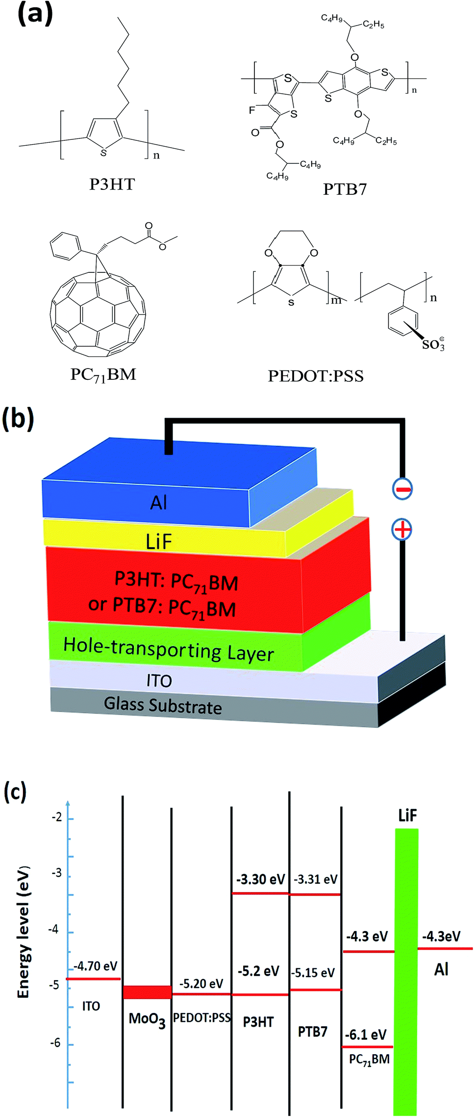 | ||
| Fig. 1 (a) The molecular structures of P3HT, PTB7, PC71BM, p-MoO3 and PEDOT:PSS. (b) The typical device structure of P3HT:PC71BM or PTB7:PC71BM polymer solar cell. (c) Energy level diagram of the component materials used.2,31 | ||
2.1 Preparation of the molybdenum solution
The synthesis was based on the preparation of the peroxomolybdic acid solution with the treatment of the ultrasonic reaction, which was very crucial for the preparation of the peroxomolybdic acid solution. First, ethanediol and isopropanol were mixed to obtain 40 mL complex-solvent by the volume ratio of 1![[thin space (1/6-em)]](https://www.rsc.org/images/entities/char_2009.gif) :9 (ethanediol to isopropanol), then 400 mg MoO3 powder reacted with 40 mL complex-solvent, and the 30% aqueous H2O2 was added to the reacted system by the volume ratio of 7:93 (H2O2 to complex-solvent). The system was dissolved completely after ultrasonication for 30 min, forming the dark blue peroxomolybdic acid organosol (inserted in Fig. 2). The molybdenum concentration was 10 mg mL−1 in mother liquor and had good dispersion and stability for several months. For each experimental run, the peroxomolybdic acid organosol was diluted with isopropanol to a certain molybdenum concentration.
:9 (ethanediol to isopropanol), then 400 mg MoO3 powder reacted with 40 mL complex-solvent, and the 30% aqueous H2O2 was added to the reacted system by the volume ratio of 7:93 (H2O2 to complex-solvent). The system was dissolved completely after ultrasonication for 30 min, forming the dark blue peroxomolybdic acid organosol (inserted in Fig. 2). The molybdenum concentration was 10 mg mL−1 in mother liquor and had good dispersion and stability for several months. For each experimental run, the peroxomolybdic acid organosol was diluted with isopropanol to a certain molybdenum concentration.
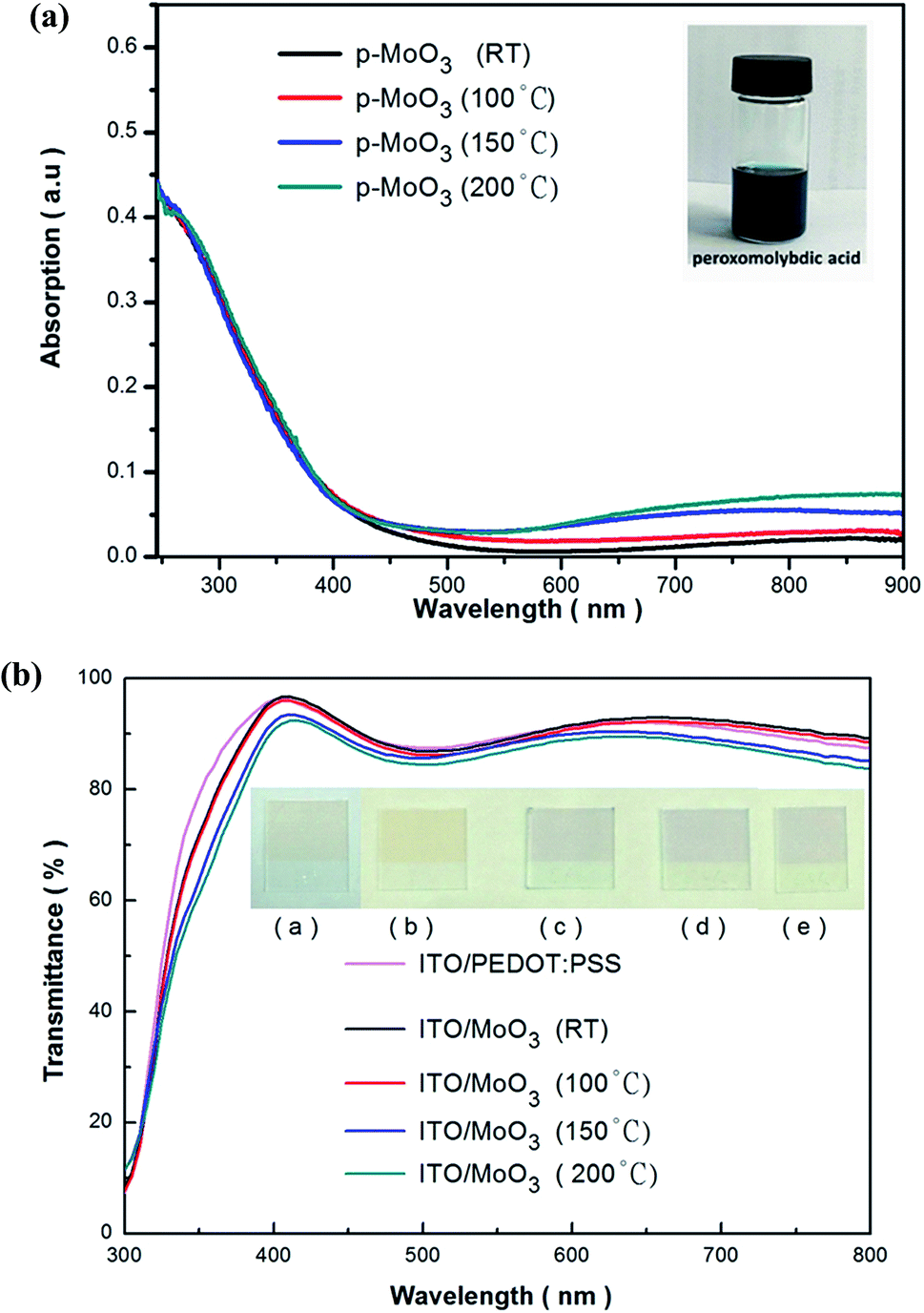 | ||
| Fig. 2 (a) UV-vis absorption spectra of the p-MoO3 thin films under various annealing temperature. (b) Transmission spectra of PEDOT:PSS thin film (a) and p-MoO3 thin films treated with room temperature drying (b), 100 °C (c), 150 °C (d), 200 °C (e). | ||
2.2 Fabrication of PSC devices
Prior to device fabrication, the solutions of light-absorbing layer were prepared. Both 1,2-dichlorobenzene solution containing P3HT and PC71BM (1:0.8, w/w) and a mixed solvent of chlorobenzene and 1,8-diiodooctane (97:3, v/v) containing PTB7:PC71BM (1:1.5, w/w) were stirred in glovebox at 60 °C overnight. Upon cooling to room temperature, the solutions were filtered through a 0.2 μm polytetrafluoroethylene (PTFE) filter before using. The ITO substrates (CSG Holding Co. Ltd., Shenzhen, China) were cleaned by sonication using detergent, deionized water, acetone and isopropanol sequentially for 15 min. After an oven drying for a few hours, the ITO surface was treated with plasma treatment for 10 min. Then the layers of PEDOT:PSS (or peroxomolybdic acid organosol) were spin-coated onto the cleaned ITO to obtain the PEDOT:PSS films (or p-MoO3 films) as an anode buffer layers at 4000 rpm for 40 s and baked at a certain annealing temperature in glovebox, and the thickness of PEDOT:PSS (or MoO3) was about 40 nm (or 10 nm). The molybdenum concentration was diluted with isopropanol to 2 mg mL−1 using mother liquor to regulate the solution viscosity. And the annealing time to construct device HTL in this study was for 20 min. Next, the active layers were spin-coated in the glovebox (O2 < 0.1 ppm, H2O < 0.1 ppm) by employing the active layer solutions. The LiF and Al electrode were deposited continuously in a deposition chamber under a basic vacuum pressure lower than 3 × 10⁻⁴ Pa. The shadow mask was used during thermal evaporation to define the active area of 0.15 cm2. All devices were unencapsulated and measured in air.
2.3 Characterization of thin film and PSC devices
All thickness measurements were analysed using alpha-step surface profiler. Structural assessments of the thin film samples under different annealing temperature via XRD was performed using a Bruker Discovery 08 with a Hi-Star area detector.The UV-vis absorption and transmittance spectra of the p-MoO3 thin films under various annealing temperature and PEDOT:PSS thin film were measured with a HP 8453 UV-vis spectrophotometer.
XPS analysis was carried out on an XPS/ESCA (electron spectroscopy for chemical analysis) instrument (Axis Ultra DLD from Kratos Inc.) utilizing a monochromatized Al Kα X-ray source. Spectra were referenced to the residual hydrocarbon contamination at 284.6 ± 0.1 eV. The thin films (ca. 40 nm) were deposited on the ITO substrate for XPS analysis.
The work functions of the p-MoO3 thin film samples under different annealing temperatures were investigated using Kelvin Probe measurements, carried out on a KP Technology SKP5050 in a glove-box filled in a conditioned chamber where the O2 level is <0.1 ppm.
Scanning electron microscope (SEM) and Tapping-mode atomic force microscope (AFM) images using a NanoScope NS3A system (Digital Instruments) were obtained to observe the surface morphology of the annealed films.
The current density–voltage (J–V) characteristics of the devices were performed using a computer controlled Keithley 2400 source-meter under illumination with calibrated AM1.5G (100 mW cm−2) at room temperature.
3. Result and discussion
3.1 Optical characteristics of MoO3 thin films
Firstly the UV-vis measurement was carried on the spin-coated thin films with the same spin-coating conditions and different annealing temperatures. As clearly shown in Fig. 2(a), all the p-MoO3 thin films are almost transparent within visible light range, and this will be of benefit for light harvesting. However, a growing small broad absorption ranging from 600 nm to 800 nm is observed for the annealed thin films under 150 °C. Increasing the treated temperature to 200 °C, this small broad absorption becomes more evident. This fascinating phenomenon may be attributed to the free electrons being trapped in oxygen vacancies in these p-MoO3 thin films.32In accordance with the condition of device fabrication, we further investigated the transmission spectra of the thin films including PEDOT:PSS film to evaluate the transparency of these films in devices (Fig. 2(b)). These films are spin-coated on ITO glasses. It is obvious that transmission values of all the films show good light transmittance except in the wavelength near 500 nm and 750 nm. This phenomenon is attributed to the transparency of ITO glass and small broad absorption mentioned above.33,34 Nevertheless, the transmission values are above 80% for all films regardless of the annealing temperature, implying that p-MoO3 thin films are qualified to be good interfacial later without significant absorption losses.
3.2 Morphology of the p-MoO3 thin film
Then XRD measurements were performed on p-MoO3 thin films deposited on ITO substrates and annealed in glovebox with different annealing temperatures. Fig. 3 shows the XRD patterns of p-MoO3 thin films that are formed at various heat treated temperatures, the p-MoO3 layers do not yield significant diffraction peaks as confirmed by XRD as shown in Fig. 3, which shows that these p-MoO3 thin films have an amorphous structure. But these p-MoO3 thin films with amorphous structure have been demonstrated to be effective to the device performance.24,25,35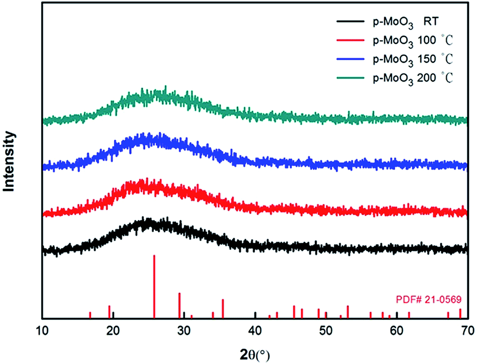 | ||
| Fig. 3 XRD pattern of the resulting p-MoO3 thin films annealed under various temperatures. | ||
To understand the surface morphology of the annealed films, SEM and AFM were performed to observe the morphology characteristics of the p-MoO3 films. Fig. 4 shows SEM images of the annealed p-MoO3 thin films with different annealing temperatures. It is clear that the surface under the condition of room temperature drying is quite uneven and not uniform with some obvious small MoO3 gains. However, it can also be noted that the surface become much flatter with the increase of heating temperature. We attribute this phenomenon to the evaporation of the solvent and progress of p-MoO3 thin film formation. When the annealing temperature is increased to 150 °C, surface topography of the p-MoO3 thin film is the most flat and uniform without any small gains. At this point, the heat treatment makes the film more compact, which prevents the current leakage of the solar cells, and is beneficial to the improvement of the devices. But further raising the annealing temperature to 200 °C, thin film appears critically gathered aggregation phenomenon and less uniform. This can be due to enhanced surface diffusion of the species leading to smaller grains joining together to grow into larger grains.
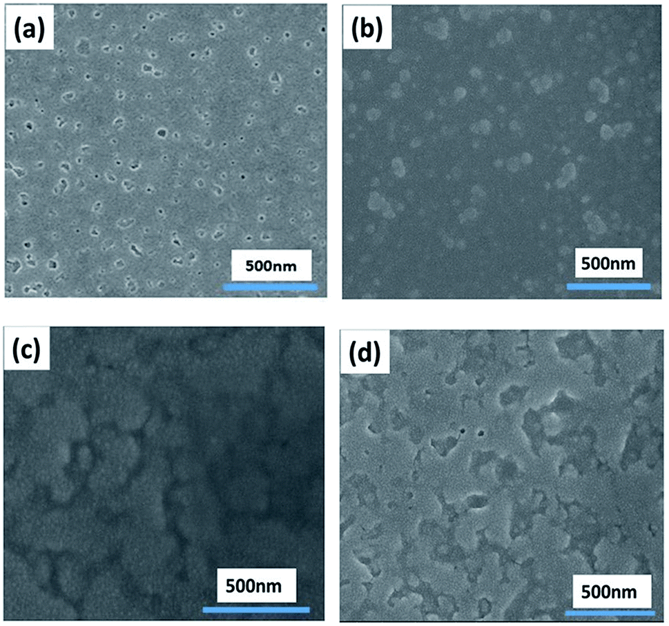 | ||
| Fig. 4 SEM images of the thin films morphology of p-MoO3 thin films morphology on ITO treated with room temperature drying (a), 100 °C (b), 150 °C (c), 200 °C (d). | ||
Fig. 5 shows AFM images of the p-MoO3 thin films with different annealing temperatures. The surface roughness (in Root Mean Square, RMS) of the p-MoO3 thin film treated with different annealing temperatures is 2.36 nm, 2.12 nm, 1.46 nm and 1.51 nm for room temperature drying, 100 °C, 150 °C and 200 °C, respectively. The p-MoO3 thin films treated with heat treatment of 150 °C possess the lowest surface roughness, which is quite well consistent with the result of SEM images. Low surface roughness of the p-MoO3 thin film suggests that they can smoothen the ITO substrate surface effectively to avoid local shorts and at the same time be dense enough to prevent the current leakage, which is prerequisites to guarantee their implementation as effective buffer layer for organic electronics.
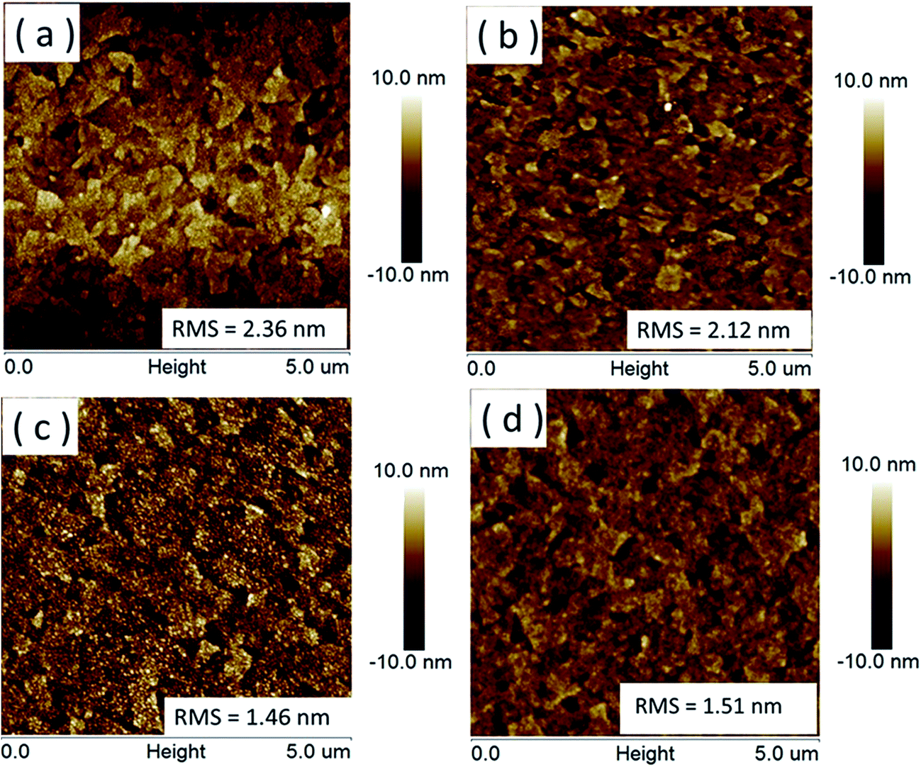 | ||
| Fig. 5 AFM morphology images of p-MoO3 thin films on ITO treated with room temperature drying (a), 100 °C (b), 150 °C (c), 200 °C (d). | ||
3.3 Components and electrical characterization of p-MoO3 thin films
X-ray photodectron spectroscopy (XPS) shown in Fig. 6 was operated to obtain the evidence for the composition of the p-MoO3 thin films treated with various annealing temperature. The binding energy (BE) obtained in the XPS analysis was corrected for specimen charge by referencing the C 1s peak to 284.6 eV. Fig. 6(a) compares the full scan spectra of the annealed p-MoO3 thin films, the characteristic peaks of the O 1s, Mo 3s, Mo 3p and Mo 3d levels are shown in the full spectra of the p-MoO3 thin films. Moreover, no other peaks of the impurity and ITO substitute are found, which suggests that the synthetic precursor can be spread uniformly and completely decomposes to p-MoO3 by annealing. In Fig. 6(b), the Mo 3d doublet presents a spin–orbit splitting between the Mo 3d3/2 and 3d5/2 bands. The Mo 3d3/2 and 3d5/2 peaks of the p-MoO3 films treated under RT and 100 °C located at 232.8 and 235.9 eV, respectively. The lines of doublet are Gaussian with the d intensity ratio of 2:3, separated by 3.1 eV. It is apparent that the position of the Mo (3d) lines is expected for Mo6+ ions as in p-MoO3.30,36,37
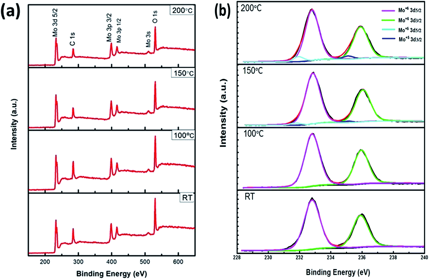 | ||
| Fig. 6 X-ray photoelectron spectroscopy of p-MoO3 thin films. (a) Full scanned spectra, (b) Mo 3d core level of thin films treated with various annealing temperature. | ||
However, two different oxidation states of Mo ions are observed with further increasing the annealing temperature to 150 °C and 200 °C, the positions of newly formed Mo5+ peaks in the 150 °C and 200 °C annealed films fitted by two 3d5/2 and 3d3/2 doublets in the form of a Gaussian function located 231.7 eV and 234.9 eV, respectively, which is identified as Mo5+.38,39 While the positions of Mo6+ peaks annealed films has not changed with further improve the annealing temperature. The calculated Mo5+/Mo6+ ratios for the 150 °C and 200 °C annealed films are 0.030 and 0.071, respectively. By using the Mo5+/Mo6+ obtained from the Mo 3d core level spectra, the estimated Mo:O stoichiometries of p-MoO3 films annealed in the 150 °C and 200 °C are 2.99 and 2.96, respectively. It can be ascribed that the concentration of the Mo5+ component in the p-MoO3 films is greatly connected with thin film processing conditions, which coincides with the fact that preparation of p-MoO3 in the oxygen deficient environment (in glovebox) and annealing temperatures led to present Mo5+ states, corresponding to the electron transfer from O 2p to Mo 4d and generation of oxygen vacancies.39–42
To further evaluate the energetics of the solution-processed p-MoO3 thin films under annealing conditions, Kelvin probe (KP) analysis was performed to obtain the work function (WF) of annealed films in glovebox referring to literature.26 Kelvin probe analysis of the PEDOT:PSS coated on ITO as a reference gives a WF of 5.20 eV, which is in agreement with the literature.2 The WF of annealed p-MoO3 thin films shows a gradual shift towards the higher values from 4.90 eV to 5.26 eV with increasing annealing temperatures from RT to 150 °C, reaching the highest WF value of 5.26 eV with 150 °C. We attribute this phenomenon to the desorption of adsorbates and evaporation of the solvent.43,44 With further increasing the annealing temperature to 200 °C, the WF value of the film decreases slightly to 5.22 eV. The main reason may be linked with the distinctly reduced cation oxidation shown in Fig. 6(b) and occupied oxygen vacancy defect states within the band that played the part of donor levels. The WF values are shown in Table 1.
| Anode interface | T (°C) | WF (eV) |
|---|---|---|
| PEDOT:PSS | 150 | 5.20 |
| p-MoO3 | RT | 4.90 |
| p-MoO3 | 100 | 5.10 |
| p-MoO3 | 150 | 5.26 |
| p-MoO3 | 200 | 5.22 |
3.4 Effect of the p-MoO3 thin film on the performance of PSCs
To investigate the effect of the p-MoO3 buffer layer on the photovoltaic performance of PSCs, firstly we selected the P3HT:PC71BM blended composite as the light-absorbing layer and constructed some solar cells. Device structures of P3HT:PC71BM solar cells fabricated with p-MoO3 thin films treated with various annealing temperatures are presented as follow:(A) ITO/PEDOT:PSS (150 °C)/P3HT:PC71BM/LiF/Al.
(B) ITO/p-MoO3 (RT)/P3HT:PC71BM/LiF/Al.
(C) ITO/p-MoO3 (100 °C)/P3HT:PC71BM/LiF/Al.
(D) ITO/p-MoO3/P3HT:PC71BM/LiF/Al.
(E) ITO/p-MoO3 (200 °C)/P3HT:PC71BM/LiF/Al.
Devices A is the control sample with a PEDOT:PSS buffer layer, devices B, C, D and E are samples with the annealed p-MoO3 layer. The device performance parameters are summarized in Table 2.
| Device | T (°C) | JSC (mA cm−2) | VOC (V) | FF (%) | Rs (Ω cm2) | Rsh (Ω cm2) | PCE (%) |
|---|---|---|---|---|---|---|---|
| A | 150 | 10.50 | 0.59 | 63.1 | 8.15 | 968.57 | 3.91 |
| B | RT | 8.49 | 0.57 | 56.9 | 10.50 | 639.03 | 2.75 |
| C | 100 | 9.42 | 0.58 | 62.0 | 8.49 | 743.94 | 3.38 |
| D | 150 | 10.70 | 0.59 | 63.7 | 8.08 | 1145.46 | 4.02 |
| E | 200 | 10.36 | 0.58 | 62.9 | 8.20 | 921.46 | 3.78 |
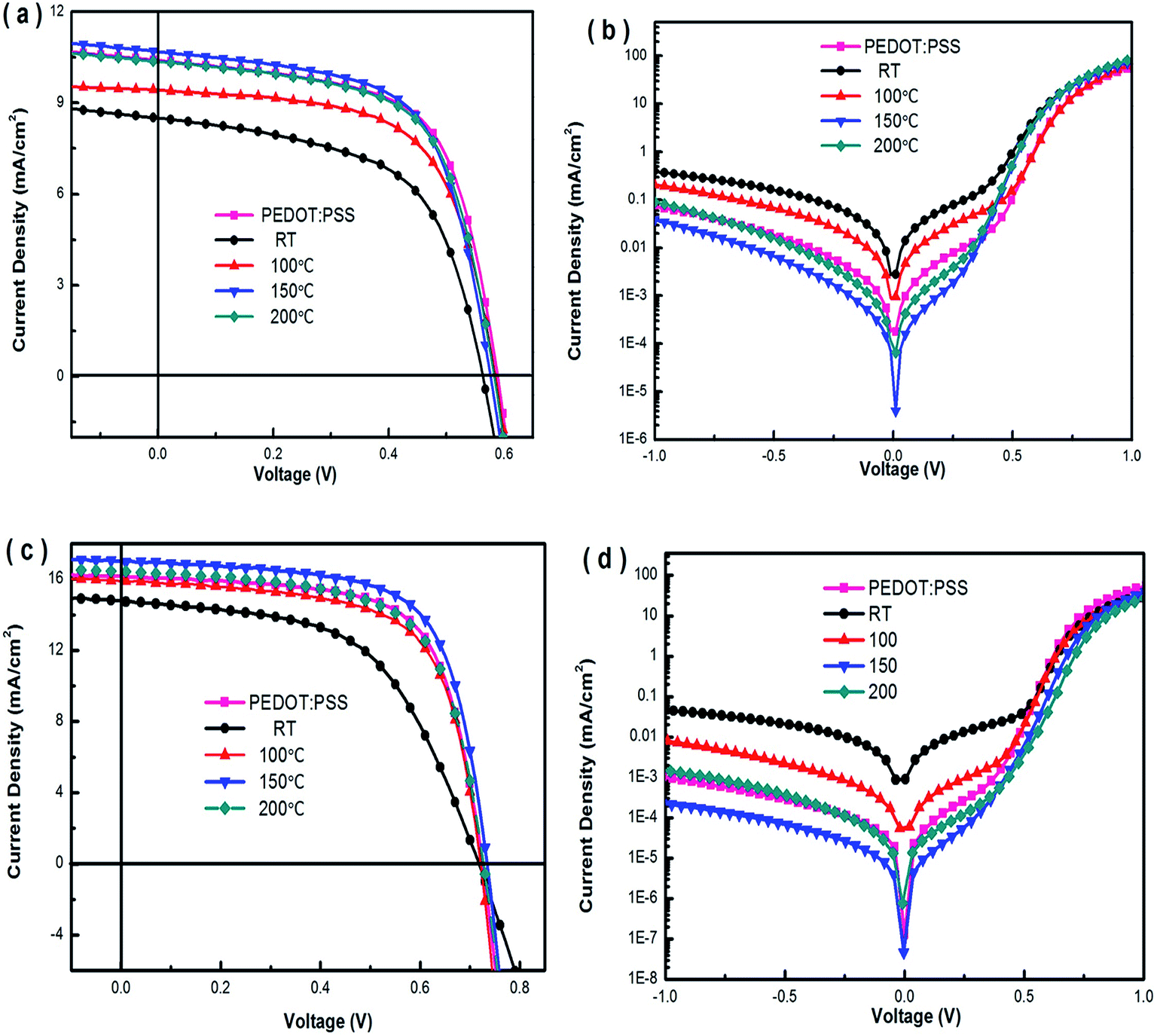
J–V curves of devices A–E under the illumination of AM1.5G, 100 mW cm−2 are depicted in Fig. 7(a). For device A with PEDOT:PSS buffer layer, it shows a PCE of 3.91% with a short-circuit current density (JSC) of 10.50 mA cm−2, an open-circuit voltage (VOC) of 0.59 V, and a fill factor (FF) of 63.1%. In contrast, the four parameters (VOC, JSC, FF, and PCE) of devices with the p-MoO3 buffer layer exhibit different degrees of growth under the annealing temperature increased from RT to 150 °C. The device with the p-MoO3 anode buffer layer annealed at 150 °C shows the best PCE of 4.02, with a VOC of 0.59 V, a JSC of 10.70 mA cm−2, and a FF of 63.7%, which is better than that using the PEDOT:PSS buffer layer (PCE = 3.91%). Further increasing the annealing temperature to 200 °C, the device performance is decreased apparently with a PCE of 3.78%, a VOC of 0.58 V, a JSC of 10.36 mA cm−2, and a FF of 62.9%.
 | ||
| Fig. 7 J–V characteristic curve of different devices fabricated with annealed p-MoO3 thin films under illumination and in the dark. (a, b) P3HT:PC71BM solar cells under illumination and in the dark, (c, d) PTB7:PC71BM solar cells under illumination and in the dark. | ||
A closer look at the J–V curves are shown in Fig. 7(b), we can find that the both reverse current density and leakage current of the devices are reduced with the increase of heat treatment p-MoO3 buffer layer, and the devices for 150 °C possess the lowest reverse current density and leakage current. This is because the 150 °C heat treatment makes the film more compact, which has fewer defects, reduces charge recombination, and is beneficial to the improvement of the devices. Moreover, the rectification ratio of the devices calculated based on the J–V curves at ±1.0 V is also calculated. For devices A, B, C, D and E, the rectification ratio is 2.2 × 10³, 2.0 × 10², 5.1 × 10², 3.1 × 10³ and 1.1 × 10³, respectively. Clearly the rectification ratio values of devices D and E with the p-MoO3 buffer layer annealed under 150 °C and 200 °C are simultaneously higher than that of device B and C with the p-MoO3 buffer layer under temperature drying and annealed under 100 °C. Series resistance Rs and shunt resistance Rsh are clear as shown in Table 2. Rsh of P3HT:PC71BM based devices with p-MoO3 buffer layer annealed at 150 °C is 1145.46 Ω cm2, which is much greater than the devices with p-MoO3 buffer layer without annealing (639.03 Ω cm2), annealed at 100 °C (743.96 Ω cm2) and at 200 °C (921.46 Ω cm2). This is presumably due to the increase of compact density of the film surface (see Fig. 4(c) and 5(c)), leading to the decrease of charge recombination and leakage current, which is also in agreement with the Fig. 7(b). Moreover, the Rs of the devices decrease with the increase of heat treatment p-MoO3 buffer layer, and the value of 8.08 Ω cm2 for the device with p-MoO3 layer annealed 150 °C is the lowest among those devices with p-MoO3 layer other heat treatment temperature. Increase of heat treatment temperature usually causes the reduction of molybdenum oxide, which leads to rise in conductivity of molybdenum oxide. In general, reduced transition metal oxides (TMOs) not only shows an increase in conductivity, but also causes stronger optical absorption.45 We attribute this interesting phenomenon to a result of the forming process of p-MoO3 and a slightly non-stoichiometric composition with some oxygen deficiency leading to reduced oxides.
The improved PCE of devices with annealed p-MoO3 hole transporting layers (HTL) may origin from the following factors; (i) the favorable surface morphology of the annealed p-MoO3 HTL. As shown in SEM images (Fig. 4) and AFM images (Fig. 5), the p-MoO3 HTL spin-coated on ITO substrates without the annealing is quite not smooth and dense compared to substrates, leading to the poor device performance. By increasing the annealing temperature, the p-MoO3 surface is growing smoother and compacter with the optimum surface and smallest roughness (RMS) of 1.46 nm for 150 °C, This decreased roughness accounts for the different dark J–V characteristics (Fig. 7(b)) of the devices with p-MoO3 layer annealed various temperatures, in which the devices exhibit increasingly excellent diode characteristics with higher rectification ratio and lower leakage current under reverse bias with improved annealing temperature. It means that the annealed p-MoO3 layer is capable of lowering the leakage current caused by the disagreeable roughness of ITO substrate. Further improving the annealing temperature leads to the slight aggregation and rising back of roughness. Therefore, the contact between the p-MoO3 layer and the active layer becomes less favorable to the hole extraction.
(ii) The formation of oxygen vacancies and the growing Mo5+ cation leading to the change of WF under the annealing. UV-vis absorption spectra analysis (Fig. 2(a)) indicates the formation of oxygen vacancies of the annealed p-MoO3 layer started with the annealing temperature 150 °C and the amount of oxygen vacancies further increased with improved temperature to 200 °C, which is all consistent with the XPS analysis as presented in Fig. 6. During annealing treatment, small amount of oxygen vacancies generated owing to the process of dehydration and desorption is capable of causing effective n-type doping for 150 °C, which is greatly conducive to the improved performance of the devices D with a PCE of 4.02%, the further increasing amount of oxygen vacancies with improved temperature to 200 °C leads to a slightly declined PCE of 3.78%. Furthermore, the oxygen ion vacancies of the substoichiometric p-MoO3 are occupied by two electrons and acted as donor centres with the donor level at 0.27 eV below the conduction band, the charge transfer from oxygen vacancies to Mo ions creates reduce d oxidation states of Mo5+. It is reported that a general correlation between cation oxidation state and an oxide's WF is that metal oxides in their more oxidized forms tend to have higher work functions than their reduced forms.43 Therefore, the increasing change of the WF from 4.90 eV to 5.22 eV under the annealing from RT to 200 °C couples with a fluctuation of the highest WF 5.26 eV for 150 °C, which influences the built-in electric field of the devices and the photocurrent being extracted efficiently at short-circuit.
In order to further testify the possibility of general usage of the p-MoO3 layer as a hole-transporting layer under the mild thermal-annealing in polymer solar cells, we also prepare the devices with the structures of PTB7:PC71BM solar cells fabricated with PEDOT:PSS and p-MoO3 thin films treated with various annealing temperatures as following:
(F) ITO/PEDOT:PSS (150 °C)/PTB7:PC71BM/LiF/Al.
(G) ITO/p-MoO3 (RT)/PTB7:PC71BM/LiF/Al.
(H) ITO/p-MoO3 (100 °C)/PTB7:PC71BM/LiF/Al.
(I) ITO/p-MoO3 (150 °C)/PTB7:PC71BM/LiF/Al.
(J) ITO/p-MoO3 (200 °C)/PTB7:PC71BM/LiF/Al.
In Fig. 7(c), the J–V characteristics of the PTB7:PC71BM devices under AM1.5G illumination are presented. It is evident that the annealing to p-MoO3 layer induces large improvement in JSC from 14.78 mA cm−2 to 16.43 mA cm−2 and FF from 54.9% to 65.1% with the annealing temperature from RT to 200 °C. The best JSC, FF and PCE of the p-MoO3-based devices is 17.02 mA cm−2, 68.1% and 8.46% for 150 °C, respectively, which apparently surpass the PEDOT-based devices with a JSC of 16.17 mA cm−2, FF of 67.2% and PCE of 7.93%. The performance parameters are summarized in Table 3.
| Device | T (°C) | JSC (mA cm−2) | VOC (V) | FF (%) | Rs (Ω cm2) | Rsh (Ω cm2) | PCE (%) |
|---|---|---|---|---|---|---|---|
| F | 150 | 16.17 | 0.73 | 67.2 | 5.05 | 1174.06 | 7.93 |
| G | RT | 14.78 | 0.72 | 54.9 | 13.35 | 705.19 | 5.85 |
| H | 100 | 15.90 | 0.72 | 66.2 | 5.21 | 827.53 | 7.57 |
| I | 150 | 17.02 | 0.73 | 68.1 | 4.49 | 1275.09 | 8.46 |
| J | 200 | 16.43 | 0.73 | 65.1 | 4.82 | 976.58 | 7.81 |
As a consequence, the devices with the p-MoO3 films annealed at 150 °C exhibit the largest increase in performance with the best PCE of 8.46%, further confirming that our prepared p-MoO3 thin films annealed at moderate temperature are fit for the PTB7:PC71BM devices due to the favorable surface morphology and electrical properties as discussed above. Meanwhile, according to the leakage dominated region (<0.5 V) as shown in Fig. 7(d), the dark current of the PTB7:PC71BM devices with the annealed p-MoO3 thin films present the trend toward miniaturization with the minimum at 150 °C, which is much less than that of the device F with PEDOT:PSS. This also indicates that p-MoO3 thin film is more efficient in hole-collection and electron-blocking when served as a HTL in PTB7:PC71BM BHJ devices.
Apart from device efficiency, device stability is another important aspect affecting the realization of commercial polymer solar. In this study, we find that the devices with p-MoO3 thin film exhibit enhanced stability. All of these devices constructed as described in Section 2.2 are not encapsulated and stored in the glovebox filled with nitrogen atmosphere (O2 < 0.1 ppm, H2O < 0.1 ppm). We choose the devices with p-MoO3 and PEDOT:PSS thin films annealed at optimal annealing temperature 150 °C as tested objects. Fig. 8 displays the PCEs and normalized PCEs as a function of aging time, of P3HT:PC71BM and PTB7:PC71BM devices incorporated p-MoO3 thin films. For P3HT:PC71BM devices as shown in Fig. 8(a), the PCEs decrease dramatically for the devices fabricated with PEDOT:PSS and reach from 3.91% to 2.40% after 60 days, only keeping about 60% of their initial efficiencies. In comparison, the p-MoO3-based P3HT:PC71BM devices get PCEs of 3.40% after storage for 60 days, remaining about 85% of their initial efficiencies (from 4.02% to 3.40%). On the other hand, Fig. 8(b) presents the stability of PTB7:PC71BM devices with different HTL. The PEDOT-based devices degrade rapidly after 60 days with about 40% decay of PCEs (from 7.93% to 4.83%), whereas the devices incorporating the p-MoO3 HTLs get only 13.3% decay of PCEs (from 8.46% to 7.33%) after 60 days, revealing the high stability of the p-MoO3 interfaces. Clearly, it is indicated that the devices incorporating the p-MoO3 thin films exhibit higher stability.
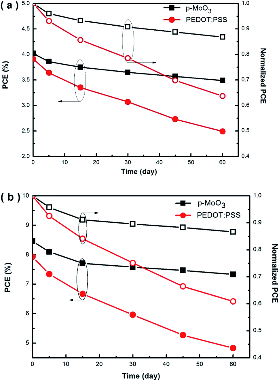 | ||
| Fig. 8 PCEs and normalized PCEs as functions of aging time of P3HT:PC71BM (a) and PTB7:PC71BM (b) devices incorporating p-MoO3 thin films. | ||
4. Conclusions
The favorably stable dark blue peroxomolybdic acid organosol is simply synthesized by the treatment of the ultrasonic reaction. The prepared p-MoO3 films were characterized from the spectroscopic measurements, SEM, AFM, XPS analysis, and Kelvin probe analysis. It is found that the favorably smooth and dense surface morphology of the p-MoO3 layers are obtained under 150 °C with the good optical and electrical properties. Furthermore, the performance of the P3HT:PC71BM and PTB7:PC71BM devices with p-MoO3 thin films is found to depend strongly on the annealing and show best performance for 150 °C. The improved performance of devices origin from the factors; (i) the favorable surface morphology of the annealed p-MoO3 films leading to higher rectification ratio and lower leakage current. (ii) The formation of oxygen vacancies and the growing Mo5+ cation leading to the change of WF under the annealing. Furthermore, the devices containing p-MoO3 thin film exhibited enhanced environmental stability. Overall, the simple and stable peroxomolybdic acid solution that we have developed is a viable candidate for replacing the PEDOT:PSS anode modifying layers in many organic solar cells including other electronic devices that require an ultrasmooth and high WF solution-processed hole selective contact.Acknowledgements
This work was financially supported by the National Natural Science Foundation of China (Grant No. 61474046 and 61176061).References
- G. Yu, J. Hummelen, F. Wudl and A. J. Heeger, Polymer photovoltaic cells: Enhanced efficiencies via a network of internal donor–acceptor heterojunctions, Science, 1995, 270, 1789–1791 CAS.
- Z. He, C. Zhong, S. Su, M. Xu, H. Wu and Y. Cao, Enhanced power-conversion efficiency in polymer solar cells using an inverted device structure, Nat. Photonics, 2012, 6, 591–595 Search PubMed.
- J. You, L. Dou, K. Yoshimura, T. Kato, K. Ohya, T. Moriarty, K. Emery, C. Chen, J. Gao, G. Li and Y. Yang, A polymer tandem solar cell with 10.6% power conversion efficiency, Nat. Commun., 2013, 4, 1446 CrossRef PubMed.
- Y. Liu, J. Zhao, Z. Li, C. Mu, W. Ma, H. Hu, K. Jiang, H. Lin, H. Ade and H. Yan, Aggregation and morphology control enables multiple cases of high-efficiency polymer solar cells, Nat. Commun., 2014, 5, 5293 CrossRef CAS PubMed.
- Z. He, B. Xiao, F. Liu, H. Wu, Y. Yang, S. Xiao, C. Wang, T. P. Russell and Y. Cao, Single-junction polymer solar cells with high efficiency and photovoltage, Nat. Photonics, 2015, 9, 174–179 CrossRef CAS.
- H. Zhou, Y. Zhang, C. Mai, S. D. Collins, G. C. Bazan, T. Nguyen and A. J. Heeger, Polymer Homo-Tandem Solar Cells with Best Efficiency of 11.3%, Adv. Mater., 2015, 27, 1767–1773 CrossRef CAS PubMed.
- A. R. M. Yusoff, D. Kim, H. P. Kim, F. K. Shneider, W. J. Silvab and J. Janga, A high efficiency solution processed polymer inverted triple-junction solar cell exhibiting a power conversion efficiency of 11.83%, Energy Environ. Sci., 2015, 8, 303–316 CAS.
- J. J. Zhao, B. Z. Xia, K. Lu, D. Deng, L. Yuan, J. Q. Zhang, L. Y. Zhu, X. W. Zhu, H. Li and Z. X. Wei, Dialkoxyphenyldithiophene-based small molecules with enhanced absorption for solution processed organic solar cells, RSC Adv., 2016, 6, 60595–60601 RSC.
- M. C. Scharber and N. S. Sariciftci, Efficiency of bulk-heterojunction organic solar cells, Prog. Polym. Sci., 2013, 38, 1929–1940 CrossRef CAS PubMed.
- X. Guo, N. Zhou, S. J. Lou, J. Smith, D. B. Tice, J. W. Hennek, R. P. Ortiz, J. T. L. Navarrete, S. Li, J. Strzalka, L. X. Chen, R. P. H. Chang, A. Facchetti and T. J. Marks, Polymer solar cells with enhanced fill factors, Nat. Photonics, 2013, 7, 825–833 CrossRef CAS.
- A. J. Heeger, 25th anniversary article: bulk heterojunction solar cells: understanding the mechanism of operation, Adv. Mater., 2014, 26, 10–28 CrossRef CAS PubMed.
- R. Steim, F. R. Kogler and C. J. Brabec, Interface materials for organic solar cells, J. Mater. Chem., 2010, 20, 2499–2512 RSC.
- J. J. Lee, S. H. Lee, F. S. Kim and J. H. Kim, Simultaneous enhancement of the efficiency and stability of organic solar cells using PEDOT:PSS grafted with a PEGME buffer layer, Org. Electron., 2015, 26, 191–199 CrossRef CAS.
- Y. Sun, J. H. Seo, C. J. Takacs, J. Seifter and A. J. Heeger, Inverted polymer solar cells integrated with a low-temperature-annealed sol-gel-derived ZnO film as an electron transport layer, Adv. Mater., 2011, 23, 1679–1683 CrossRef CAS PubMed.
- L. Zhang, L. Favereau, Y. Farre, A. Maufroy, Y. Pellegrin, E. Blart, M. Hissler, D. Jacquemin, F. Odobel and L. Hammarstrom, Molecular-structure control of electron transfer dynamics of push-pull porphyrins as sensitizers for NiO based dye sensitized solar cells, RSC Adv., 2016, 6, 77184–77194 RSC.
- J. Zhang, J. Wang, Y. Fu, B. Zhanga and Z. Xie, Efficient and stable polymer solar cells with annealing-free solution-processible NiO nanoparticles as anode buffer layers, J. Mater. Chem. C, 2014, 2, 8295–8302 RSC.
- D. Zhao, S. T. Tan, L. Ke and D. L. Kwong, Optimization of an inverted organic solar cell, Sol. Energy Mater. Sol. Cells, 2010, 94, 985–991 CrossRef CAS.
- Y. Sun, C. J. Takacs, S. R. Cowan, J. H. Seo, X. Gong, A. Roy and A. J. Heeger, Efficient, Air-Stable Bulk Heterojunction Polymer Solar Cells Using MoOx as the Anode Interfacial Layer, Adv. Mater., 2011, 23, 2226–2230 CrossRef CAS PubMed.
- K. Shen, R. Yang, D. Wang and K. Ho, Stable CdTe solar cell with V2O5 as a back contact buffer layer, Sol. Energy Mater. Sol. Cells, 2016, 144, 500–508 CrossRef CAS.
- T. Stubhan, N. Li, N. A. Luechinger, S. C. Halim, G. J. Matt and C. J. Brabec, High fill factor polymer solar cells incorporating a low temperature solution processed WO3 hole extraction layer, Adv. Energy Mater., 2012, 2, 1433–1438 CrossRef CAS.
- X. B. Chu, M. Guan, Y. Zhang, Y. Y. Li, X. F. Liu and Y. P. Zeng, ITO-free and air stable organic light-emitting diodes using MoO3:PTCDA modified Al as semitransparent anode, RSC Adv., 2013, 3, 9509–9513 RSC.
- K. H. Wong, K. Ananthanarayanan, J. Luther and P. Balaya, Origin of hole selectivity and the role of defects in low-temperature solution-processed molybdenum oxide interfacial layer for organic solar cells, J. Phys. Chem. C, 2012, 116, 16346–16351 CAS.
- S. Murase and Y. Yang, Solution processed MoO3 interfacial layer for organic photovoltaics prepared by a facile synthesis method, Adv. Mater., 2012, 24, 2459–2462 CrossRef CAS PubMed.
- K. Zilberberg, H. Gharbi, A. Behrendt, S. Trost and T. Riedl, Low-temperature, solution-processed MoOx for efficient and stable organic solar cells, ACS Appl. Mater. Interfaces, 2012, 4, 1164–1168 CAS.
- Z. Tan, D. Qian, W. Zhang, L. Li, Y. Ding, Q. Xu, F. Wang and Y. Li, Efficient and stable polymer solar cells with solution-processed molybdenum oxide interfacial layer, J. Mater. Chem. A, 2013, 1, 657–664 CAS.
- S. R. Hammond, J. Meyer, N. E. Widjonarko, P. F. Ndione, A. K. Sigdel, A. Garcia, A. Miedaner, M. T. Lloyd, A. Kahn, D. S. Ginley, J. J. Berry and D. C. Olson, Low-temperature, solution-processed molybdenum oxide hole-collection layer for organic photovoltaics, J. Mater. Chem., 2012, 22, 3249–3254 RSC.
- J. Meyer, R. Khalandovsky and P. Görrn, MoO3 Films Spin-Coated from a Nanoparticle Suspension for Efficient Hole-Injection in Organic Electronics, Adv. Mater., 2011, 23, 70–73 CrossRef CAS PubMed.
- M. Xu, L. Cui, X. Zhu and L. S. Liao, Aqueous solution-processed MoO3 as an effective interfacial layer in polymer/fullerene based organic solar cells, Org. Electron., 2013, 14, 657–664 CrossRef CAS.
- S. Lin, C. Wang, K. Kao, Y. Chen and C. Liu, Electrochromic properties of MoO3 thin films derived by a sol–gel process, J. Sol-Gel Sci. Technol., 2010, 53, 51–58 CrossRef CAS.
- C. Girotto, E. Voroshazi, D. Cheyns, P. Heremans and B. P. Rand, Solution-processed MoO3 thin films as a hole-injection layer for organic solar cells, ACS Appl. Mater. Interfaces, 2011, 3, 3244–3247 CAS.
- F. Cheng, G. Fang, X. Fan and Y. Li, Enhancing the performance of P3HT:ICBA based polymer solar cells using LiF as electron collecting buffer layer and UV-ozone treated MoO3 as hole collecting buffer layer, Sol. Energy Mater. Sol. Cells, 2013, 110, 63–68 CrossRef CAS.
- T. Yang, M. Wang, Y. Cao, F. Huang, L. Huang, J. Peng, X. Gong, S. Z. D. Cheng and Y. Cao, Polymer Solar Cells with a Low-Temperature-Annealed Sol-Gel-Derived MoOx Film as a Hole Extraction Layer, Adv. Energy Mater., 2012, 2, 523–527 CrossRef CAS.
- R. A. Afre, Y. Hayashi and T. Soga, Enhanced photovoltaic device performance upon modification of indium tin oxide coated glass by liquid nitrogen treatment, J. Phys. D: Appl. Phys., 2009, 42, 042002 CrossRef.
- L. Cattin, F. Dahou, Y. Lare, M. Morsli, R. Tricot, S. Houari, A. Mokrani, K. Jondo, A. Khelil, K. Napo and J. C. Bernède, MoO3 surface passivation of the transparent anode in organic solar cells using ultrathin films, J. Appl. Phys., 2009, 105, 034507 CrossRef.
- X. Yu, T. J. Marks and A. Facchetti, Metal oxides for optoelectronic applications, Nat. Mater., 2016, 15, 383–396 CrossRef CAS PubMed.
- F. Xie, W. C. H. Choy, C. Wang, X. Li, S. Zhang and J. Hou, Low Temperature Solution Processed Hydrogen Molybdenum and Vanadium Bronzes for an Efficient Hole Transport Layer in Organic Electronics, Adv. Mater., 2013, 25, 2051–2055 CrossRef CAS PubMed.
- S. Kato, R. Ishikawa, Y. Kubo, H. Shirai and K. Ueno, Efficient Organic Photovoltaic Cells Using Hole-Transporting MoO3 Buffer Layers Converted from Solution-Processed MoS2 Films, Jpn. J. Appl. Phys., 2011, 50, 071604 CrossRef.
- M. A. Moraes, B. C. Trasferetti, F. P. Rouxinol, R. Landers, S. F. Durrant, J. Scarmínio and A. Urbano, Molybdenum oxide thin films obtained by the hot-filament metal oxide deposition technique, Chem. Mater., 2004, 16, 513–520 CrossRef.
- M. Anwar, C. A. Hogarth and R. Bulpett, Effect of substrate temperature and film thickness on the surface structure of some thin amorphous films of MoO3 studied by X-ray photoelectron spectroscopy (ESCA), J. Mater. Sci., 1989, 24, 3087–3090 CrossRef CAS.
- J. J. Jasieniak, J. Seifter, J. Jo, T. Mates and A. J. Heeger, A Solution-Processed MoOx Anode Interlayer for Use within Organic Photovoltaic Devices, Adv. Funct. Mater., 2012, 22, 2594–2605 CrossRef CAS.
- Y. Lee, J. Yi, G. F. Gao, H. Koerner, K. Park, J. Wang, K. Luo, R. A. Vaia and J. W. P. Hsu, Low-Temperature Solution-Processed Molybdenum Oxide Nanoparticle Hole Transport Layers for Organic Photovoltaic Devices, Adv. Energy Mater., 2012, 2, 1193–1197 CrossRef CAS.
- K. Kanaia, K. Koizumib, S. Ouchic, Y. Tsukamotoc, K. Sakanouec, Y. Ouchib and K. Sekib, Electronic structure of anode interface with molybdenum oxide buffer layer, Org. Electron., 2010, 11, 188–194 CrossRef.
- M. T. Greiner, L. Chai, M. G. Helander, W. Tang and Z. Lu, Transition Metal Oxide Work Functions: The Influence of Cation Oxidation State and Oxygen Vacancies, Adv. Funct. Mater., 2012, 22, 4557–4568 CrossRef CAS.
- Irfan, H. Ding, Y. Gao, C. Small, D. Y. Kim, J. Subbiah and F. So, Energy level evolution of air and oxygen exposed molybdenum trioxide films, Appl. Phys. Lett., 2010, 96, 243307 CrossRef.
- J. Meyer, S. Hamwi, M. Kröger, W. Kowalsky, T. Riedl and A. Kahn, Transition metal oxides for organic electronics: energetics, device physics and applications, Adv. Mater., 2012, 24, 5408–5427 CrossRef CAS PubMed.
| This journal is © The Royal Society of Chemistry 2017 |