
 Open Access Article
 This Open Access Article is licensed under a
 Creative Commons Attribution 3.0 Unported Licence
Modification of thermal conductivity and thermal boundary resistance of amorphous Si thin films by Al doping
Tianzhuo Zhan *a,
Masahiro Gotoa,
Yibin Xua,
Yohei Kinoshitab,
Mamoru Ishikiriyamab and
Chikashi Nishimuraa
*a,
Masahiro Gotoa,
Yibin Xua,
Yohei Kinoshitab,
Mamoru Ishikiriyamab and
Chikashi Nishimuraa
aNational Institute for Materials Science, 1-2-1 Sengen, Tsukuba 305-0047, Japan. E-mail: ZHAN.Tianzhuo@nims.go.jp
bToyota Motor Corporation, 1200, Mishuku, Susono-city, Shizuoka 410-1195, Japan
First published on 23rd January 2017
Abstract
We investigate the effects of Al doping on the thermal conductivity and thermal boundary resistance of a-Si thin films. Au/Al-doped a-Si/Si structures were prepared by depositing Al-doped amorphous Si films of different Al doping concentrations and thickness on Si substrates by magnetron sputtering. The thermal resistances of the structures were measured to calculate the thermal conductivities of the films. The thermal conductivities of the 150 nm-thick films were higher than those of 100 nm-thick films, and a sharp increase in thermal conductivity with increasing Al doping concentration was observed in the 150 nm-thick films but not in the 100 nm-thick films. Furthermore, the thermal boundary resistances at the two interfaces in the structures also increased with increasing Al doping concentration. Our findings could be used to tailor the thermal resistance of materials for thermal management in semiconductor devices as well as for development of thermal barrier coatings and thermoelectric materials with good performance.
Introduction
Amorphous Si (a-Si) has previously been difficult to dope due to its high defect density, which has prevented the application of a-Si in semiconductor devices.1 Since the discovery of hydrogenated amorphous Si and the ability to efficiently dope this material, a-Si has become widely used in various semiconductor devices such as photovoltaic solar cells, thin-film transistors, image sensors, and data memories.2 For example, the use of a-Si thin films has enabled low-cost mass production of photovoltaic solar cells, because a-Si can be deposited at very low temperatures on inexpensive large-area substrates such as glasses and plastics.3 In addition to semiconductor device applications, a-Si also shows great potential in thermoelectric applications due to its low thermal conductivity. Although the electrical and optical properties of amorphous semiconductors have been studied extensively, the thermal properties have not been thoroughly investigated.4–7 Thermal transport in amorphous solids is quite different from crystalline materials, and the phonon-gas model is no longer valid in amorphous solids. Various theoretical models such as the Einstein model,8 the minimum thermal conductivity model,9 the fraction model,10 and the diffusion model11,12 have been proposed to describe thermal transport in amorphous solids. Despite these theoretical models, experimental studies on the thermal conductivities of amorphous solids are still limited. Furthermore, thermal boundary resistance, which plays an important role in nanostructured materials that have many interfaces,13–15 is even less explored than thermal conductivity. Investigation of the thermal conductivity and thermal boundary resistance of a-Si-based materials is crucial for thermal management in semiconductor devices and for the development of efficient thermal barrier coatings and thermoelectric materials.In this study, we investigate the effects of Al doping on the thermal conductivity and thermal boundary resistance of a-Si thin films. We deposited Al-doped a-Si thin films of different Al doping concentrations and thickness on Si substrate by magnetron sputtering and then deposited an Au film on top of the films. We then measured the thermal resistances of the Au/Al-doped a-Si/Si structures to calculate the thermal conductivities of the Al-doped a-Si thin films. We found that the thermal conductivities of 150 nm-thick films are higher than those of the corresponding 100 nm-thick films at the same Al doping concentration. Furthermore, as the Al doping concentration increases, a sharp increase in thermal conductivity is observed in the 150 nm-thick films, but not in the 100 nm-thick films. Furthermore, the thermal boundary resistances at the two interfaces in the structures also increase with increasing Al doping concentration. We discuss the underlying mechanisms of the results.
Experimental
Al-doped a-Si thin films were deposited on intrinsic single crystalline Si substrate (0.5 mm thick) by RF magnetron sputtering using a laboratory-built combinatorial sputtering system with a floating potential during the coating process.16 The vacuum chamber of the sputtering system was evacuated to under a base pressure of 5.0 × 10⁻⁵ Pa. The thin films were deposited at a low substrate temperature (25 °C) in order to obtain amorphous films. The thin films were deposited using two magnetron sputter cathodes in the system. Sputtering targets of Si and Al (diameter: 50 mm, thickness: 6 mm, 99.999% (Si) 99.9999% (Al) purity, High Purity Chemical Co.) with argon gas (over 99.999% purity) were used for sputtering. The low base pressure and high purity argon gas help prevent incorporation of impurities into the growing film. The working pressure of the gas was fixed at 0.4 Pa during the process, which was automatically controlled by a control gate valve combined with a capacitance manometer. The RF power for the sputter cathode of Si was fixed at 100 W and the power for Al was varied for changing the Al doping concentration. The sputter rate of Si and Al was precisely controlled by a crystal membrane microbalance monitor. The distance between the sample and the targets of Si and Al were fixed at 173 mm and 200 mm, respectively. The 2–3 nm thick native oxide layers on the Si substrates were not removed prior to deposition of the Al-doped a-Si thin films. The Al doping concentrations of the films were 1.75%, 5%, and 10%. The Al doping concentration was varied to alter the microstructure of the amorphous thin films and the interfacial properties of the two interfaces. The film thicknesses were 50, 100, and 150 nm at each Al doping concentration. A 150 nm thick Au film was then deposited on the Al-doped a-Si films at 25 °C by magnetron sputtering to act as a laser absorber and temperature sensor.The thermal resistances of the Au/Al-doped a-Si/Si structures were measured by using the frequency domain thermoreflectance method (ω method) under vacuum (<0.02 Pa). The sample is set horizontally on the sample stage. The thermoelectric cooler system keeps the sample stage at a constant temperature (25 °C). The Au film was heated by a pump laser with angular frequency ω; the pump laser is a multimode diode laser with a wavelength of 405 nm and an output power of 360 mW. The pump laser is modulated by the TTL signal from the function generator built in the digital signal processor lock-in amplifier (Stanford SR8300). The amplitude of the ac-temperature response is about 1 K. The temperature response at the surface of the Au film was measured by a probe laser by the thermoreflectance technique. The probe laser is a single mode diode laser with a wavelength of 635 nm and an output power of 5 mW. The probe laser beams are detected by the photodiode sensor. Fig. 1 shows a schematic of the fabricated structure and the measurement technique. The temperature at the surface of the Au film T(0) can be obtained using the one-dimensional heat conduction model by the following equation:17–19
 | (1) |
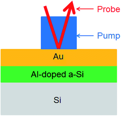 | ||
| Fig. 1 Schematic illustration of the Au/Al-doped a-Si/Si structure and thermal conductivity measurement technique. | ||
Here, d is the film thickness, q is the heat flux, λ is the thermal conductivity, C is the volumetric heat capacity. Subscripts 0, 1, and 2 denote the Au film, the Al-doped a-Si thin film, and the substrate, respectively, and R01 and R12 are the thermal boundary resistance at the Au/Al-doped a-Si thin film and Al-doped a-Si thin film/substrate interfaces, respectively. The fourth and fifth terms on the right-hand side are the thermal resistance of the Al-doped a-Si thin film and Au film, respectively. A plot of T(0)/(qd0) versus ω−1/2 gives a straight line where the y-intercept equals the total thermal resistance R of the Au/Al-doped a-Si/Si structure. We measure R of the samples with different Al-doped a-Si film thicknesses d, and plot R as a function of d. The thermal conductivity of Al-doped a-Si thin film for various Al doping concentrations was calculated from the slope of the straight line fitted to the data points for each doping concentration. The slope of the line equals to  , and with C1, C2, and λ2 known, we can calculate the thermal conductivities of the films. The thermophysical properties of the materials used in this study are listed in Table 1. Although the thermal conductivity and volumetric heat capacity of Au film may have some changes depending on the microstructure of the film, it does not significantly affect the result of R because the value of fifth term is on the order of 10−9 m2 K W−1, which is significantly smaller than R. The volumetric heat capacity of Al21 and a-Si22 are 2.43 and 1.61 × 10⁶ J m−3 K−1, respectively. The volumetric heat capacity of Al-doped a-Si films with Al doping concentration of 1.75%, 5% and 10% are calculated to 1.62, 1.65 and 1.69 × 10⁶ J m−3 K−1, respectively. Measurements were carried out at angular frequencies of 1, 2, 4 and 8 kHz and at three different locations on each sample, with each measurement performed three times to reduce error.
Results and discussion
Fig. 2 shows the measured thermal resistances of the Au/Al-doped a-Si/Si structures of different Al doping concentrations as a function of film thickness. For a fixed Al doping concentration, the three data points are expected to lie on a straight line if the films of different thicknesses have the same thermal conductivity. However, the data points for the 150 nm-thick films deviate from the linear fits (dashed lines). This indicates that the 100 and 150 nm-thick films have different thermal conductivities. This result is similar to the results for a-Si and a-Ge from previous reports.23–29 Previous work shows that the thermal conductivity of a-Si films with thicknesses less than 100 nm do not show observable film size dependence.24 If we assume this remains true for our Al-doped a-Si films, by fitting the two data points (50 and 100 nm, 50 and 150 nm) for each Al doping concentration, we can calculate the thermal conductivities of the 100 and 150 nm-thick films. Fig. 3 shows the thermal conductivities of the 100 and 150 nm-thick films as a function of Al doping concentration. It is evident that the thermal conductivities of the 150 nm-thick films are higher than those of the corresponding 100 nm-thick films at the same Al doping concentration. The 150 nm-thick films also exhibit thermal conductivity that is more strongly dependent on Al doping concentration. The thermal conductivity in the 150 nm-thick films increased sharply as the Al doping concentration increased, whereas the thermal conductivity in the 100 nm-thick films increased only slightly. For comparison, the thermal conductivity of the 100 nm-thick undoped a-Si thin film measured in our previous work26 was 0.93 W m−1 K−1, which is similar to the conductivity of the 100 nm-thick Al-doped a-Si thin films.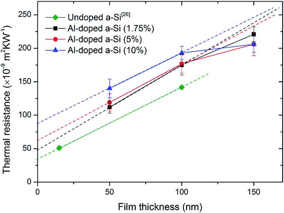 | ||
| Fig. 2 Measured thermal resistance of Au/doped a-Si/Si structures with different Al doping concentration as a function of film thickness. Thermal resistances of the Au/a-Si/Si structures measured in our previous work are also included for comparison. | ||
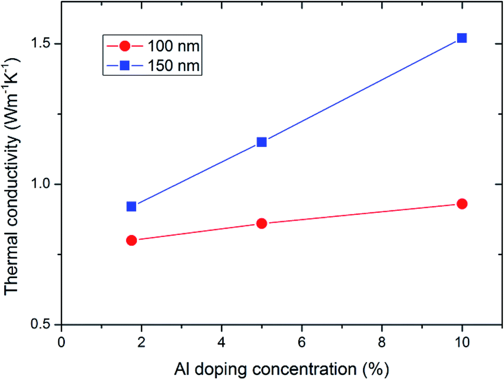 | ||
| Fig. 3 Thermal conductivities of the 100 and 150 nm-thick Al-doped a-Si films as a function of Al doping concentration. | ||
We next discuss the underlying mechanisms of change in the thermal conductivity by doping with Al. In semiconductors and insulators, heat is transported predominantly by phonons. However, doping with Al may modify the electrical conductivity of the a-Si thin films, and thus heat transport by electrons also needs to be considered. Although we did not measure the electrical conductivity of the Al-doped a-Si thin films, previous work30 has reported that hydrogenated a-Si films with an Al doping concentration of 15% have an electrical conductivity of approximately 10−5 Ω−1 m−1. This value is about two orders of magnitude higher than that of the undoped hydrogenated a-Si film, but still two orders of magnitude lower than that of crystalline Si (approximately 10−3 Ω−1 m−1). The contribution of electrons to the heat transport in Al-doped a-Si can thus be ignored. For heat transport by phonons, thermal conductivity depends on how far phonons travel between scattering events, that is, on the mean free path (MFP) of the phonons.21 Thus, changes in the thermal conductivity of a-Si thin films may be induced by changes in the phonon MFP due to doping with Al. Previous works have shown that phonons with MFPs longer than 100 nm contribute to the thermal conductivity in a-Si.23–26 In 100 and 150 nm-thick films, boundary scattering limits the MFPs of these phonons to 100 nm and 150 nm, respectively. This could explain why the 150 nm-thick films had a higher thermal conductivity than the 100 nm-thick films. Furthermore, we observed that thermal conductivity in the 150 nm-thick films increased sharply as the Al doping concentration increased. This indicates that doping with Al increased the number of phonons with MFPs longer than 100 nm. However, in the 100 nm-thick films, the MFPs of these increased phonons are limited to 100 nm by boundary scattering. Furthermore, we observed that the measured thermal conductivity in the 100 nm-thick films increased slightly as the Al doping concentration increased. This indicates that the effect of Al doping on the number of phonons with MFPs shorter than 100 nm is slight. This is in good agreement with the results of previous work,28 which found that only propagons (phonon-like propagating modes) with MFPs greater than 100 nm contribute significantly to thermal conductivity in a-Si. For films with thicknesses less than 100 nm, the thermal conductivity is dominated by diffusons (non-propagating delocalized modes). Also, previous study showed that Ga atoms decreased the thermal conductivity of solid-phase epitaxy Si layer by acting as phonon scatters.31 By contrast; in our study the Al atoms played a totally different role in a-Si. Al atoms increased the thermal conductivity of a-Si thin films by increasing the number of phonons with long MFPs.
The thermal boundary resistances at the two interfaces of the structures are the intercepts of the linear fits (dashed lines in Fig. 2). It can be clearly seen that the thermal boundary resistances of Al-doped samples were higher than undoped samples and increase with increasing Al doping concentration. Thermal boundary resistance is attributed to the mismatch between the phonon spectra of the materials on both sides of the interface. The diffuse mismatch model (DMM) provides a quick and simple way to predict thermal boundary resistance from the mismatch between phonon spectra. The Debye temperature plays an important role in determining the phonon spectra in materials. Thus, materials on both sides of the interface with larger difference in Debye temperature typically have larger thermal boundary resistance. The Debye temperatures of a-Si and Al are 487 K (ref. 23) and 428 K, respectively. The Debye temperature of Al-doped a-Si films (a-Si1−xAlx) can thus be estimated by the equation θD = (487 − 59x) K.32 When the Al doping concentration is 10%, the Debye temperature of the Al-doped a-Si film is estimated to be 481 K, indicating that the change in Debye temperature induced by doping with Al is extremely small. This indicates that the DMM model fails to explain the significant enhancement of the thermal boundary resistance. It is known that, in addition to the mismatch of phonon spectra, interfacial properties such as interfacial roughness, interdiffusion, bonding strength, and interface chemistry also have a considerable effect on thermal boundary resistance,33–36 and these effects are not considered in the DMM model. Thus, we speculate that the interfacial properties at the two interfaces were modified by doping with Al, resulting in the enhancement of the thermal boundary resistance.
Conclusions
In summary, we investigated the effects of Al doping on the thermal conductivity and thermal boundary resistance of a-Si thin films. We found that the thermal conductivities of 150 nm-thick films were higher than the corresponding 100 nm-thick films with the same Al doping concentration, indicating that phonons with MFPs longer than 100 nm contribute to the thermal conductivity in Al-doped a-Si films. As the Al doping concentration increased, the thermal conductivities of the 150 nm-thick films increased sharply, a phenomenon that was not observed in the 100 nm-thick films. This indicates that phonons with MFPs shorter than 100 nm are not greatly affected by Al doping. Furthermore, the thermal boundary resistance at the two interfaces also increased with increasing Al doping concentration. We speculate that the increase in the thermal boundary resistance is caused by modification of the interfacial properties at the two interfaces due to Al doping. The doping with Al modified both the thermal conductivity and thermal boundary resistance of the a-Si thin films, and this could be used to tailor the thermal resistance of a-Si based materials and structures for thermal management in semiconductor devices as well as for development of thermal barrier coatings and thermoelectric materials with good performance.References
- R. A. Street, Hydrogenated Amorphous Silicon, Cambridge University Press, 1991 Search PubMed.
- P. K. Shufflebotham, H. C. Card and A. Thanailakis, J. Non-Cryst. Solids, 1987, 92, 183–244 CrossRef CAS.
- A. Shah, J. Meier, A. Buechel, U. Kroll, J. Steinhauser, F. Meillaud, H. Schade and D. Domine, Thin Solid Films, 2006, 502, 292–299 CrossRef CAS.
- D. G. Cahill, M. Katiyar and J. R. Abelson, Phys. Rev. B: Condens. Matter Mater. Phys., 1994, 50, 6077–6081 CrossRef CAS.
- X. Liu, J. L. Feldman, D. G. Cahill, R. S. Crandall, N. Bernstein, D. M. Photiadis, M. J. Mehl and D. A. Papaconstantopoulos, Phys. Rev. Lett., 2009, 102, 035901 CrossRef PubMed.
- B. L. Zink, R. Pietri and F. Hellman, Phys. Rev. Lett., 2006, 96, 055902 CrossRef CAS PubMed.
- R. Sultan, A. D. Avery, J. M. Underwood, S. J. Mason, D. Bassett and B. L. Zink, Phys. Rev. B: Condens. Matter Mater. Phys., 2013, 87, 214305 CrossRef.
- A. Einstein, Ann. Phys., 1911, 35, 679–694 CAS.
- G. A. Slack, in Solid State Physics: Advances in Research and Applications, ed. H. Ehrenreich, et al., Academic, New York, 1979, vol. 34, p. 1 Search PubMed.
- S. Alexander, O. E. Wohlman and R. Orbach, Phys. Rev. B: Condens. Matter Mater. Phys., 1986, 34, 2726–2734 CrossRef.
- P. B. Allen and J. L. Feldman, Phys. Rev. Lett., 1989, 62, 645–648 CrossRef CAS PubMed.
- J. L. Feldman, M. D. Kluge, P. B. Allen and F. Wooten, Phys. Rev. B: Condens. Matter Mater. Phys., 1993, 48, 12589–12602 CrossRef.
- P. J. O'Brien, S. Shenogin, J. Liu, P. K. Chow, D. Laurencin, P. H. Mutin, M. Yamaguchi, P. Keblinski and G. Ramanath, Nat. Mater., 2013, 12, 118–122 CrossRef PubMed.
- G. Pernot, M. Stoffel, I. Savic, F. Pezzoli and P. Chen, et al., Nat. Mater., 2010, 9, 491–495 CrossRef CAS PubMed.
- M. D. Losego, M. E. Grady, N. R. Sottos, D. G. Cahill and P. V. Braun, Nat. Mater., 2012, 11, 502–506 CrossRef CAS PubMed.
- M. Goto, A. Kasahara and M. Tosa, Appl. Surf. Sci., 2006, 252, 2482–2487 CrossRef CAS.
- Y. Xu, R. Kato and M. Goto, J. Appl. Phys., 2010, 108, 104317 CrossRef.
- Y. Xu, M. Goto, R. Kato, Y. Tanaka and Y. Kagawa, J. Appl. Phys., 2012, 111, 084320 CrossRef.
- T. Zhan, Y. Xu, M. Goto, Y. Tanaka, R. Kato and M. Sasaki, RSC Adv., 2015, 5, 49703–49707 RSC.
- R. Kato and I. Hatta, Int. J. Thermophys., 2005, 26, 179–190 CrossRef CAS.
- Japanese society of thermophysical, Thermophysical Properties Handbook, Japanese Thermophysical Society, Yokendo, Ltd, 1990 Search PubMed.
- B. L. Zink, R. Pietri and F. Hellman, Phys. Rev. Lett., 2006, 96, 055902 CrossRef CAS PubMed.
- X. Liu, J. L. Feldman, D. G. Cahill, R. S. Crandall, N. Bernstein, D. M. Photiadis, M. J. Mehl and D. A. Papaconstantopoulos, Phys. Rev. Lett., 2009, 102, 035901 CrossRef PubMed.
- H. S. Yang, D. G. Cahill, X. Liu, J. L. Feldman, R. S. Crandall, B. A. Sperling and J. R. Abelson, Phys. Rev. B: Condens. Matter Mater. Phys., 2010, 81, 104203 CrossRef.
- K. T. Regner, D. P. Sellan, Z. H. Su, C. H. Amon, A. J. H. McGaughey and J. A. Malen, Nat. Commun., 2013, 4, 1640 CrossRef PubMed.
- T. Zhan, Y. Xu, M. Goto, Y. Tanaka, R. Kato, M. Sasaki and Y. Kagawa, Appl. Phys. Lett., 2014, 104, 071911 CrossRef.
- T. Zhan, Y. Xu, M. Goto, Y. Tanaka, R. Kato, M. Sasaki and Y. Kagawa, AIP Adv., 2014, 4, 027126 CrossRef.
- J. L. Braun, C. H. Baker, A. Giri, M. Elahi, K. Artyushkova, T. E. Beechem, P. M. Norris, Z. C. Leseman, J. T. Gaskins and P. E. Hopkins, Phys. Rev. B: Condens. Matter Mater. Phys., 2016, 93, 140201 CrossRef.
- J. M. Larkin and A. J. H. McGaughey, Phys. Rev. B: Condens. Matter Mater. Phys., 2016, 89, 144303 CrossRef.
- M. Yamaguchi, J. Non-Cryst. Solids, 1985, 77–78, 535–538 CrossRef CAS.
- T. Ueda, S. Sakane, T. Ishibe, K. Watanabe, S. Takeuchi, A. Sakai and Y. Nakamura, J. Electron. Mater., 2016, 45, 1914–1920 CrossRef CAS.
- F. Schaffler, in Properties of advanced semiconductor materials GaN, AlN, InN, BN, SiC, SiGe, ed. M. E. Levinshtein, S. L. Rumyantsev and M. S. Shur, John Wiley & Sons, Inc., New York, 2001, pp. 149–188 Search PubMed.
- J. C. Duda and P. E. Hopkins, Appl. Phys. Lett., 2012, 100, 111602 CrossRef.
- P. E. Hopkins, J. C. Duda, C. W. Petz and J. A. Floro, Phys. Rev. B: Condens. Matter Mater. Phys., 2011, 4, 035438 CrossRef.
- J. C. Duda, C.-Y. P. Yang, B. M. Foley, R. Cheaito, D. L. Medlin, R. E. Jones and P. E. Hopkins, Appl. Phys. Lett., 2013, 102, 081902 CrossRef.
- B. Gotsmann and M. A. Lantz, Nat. Mater., 2012, 12, 59–65 CrossRef PubMed.
| This journal is © The Royal Society of Chemistry 2017 |