
 Open Access Article
 This Open Access Article is licensed under a
 Creative Commons Attribution 3.0 Unported Licence
Epitaxial growth and cationic exchange properties of layered KNb3O8 thin films†
A. Waroqueta,
V. Demange *a,
N. Hakmeha,
J. Perrièreb,
S. Freslona,
S. Députierb and
M. Guilloux-Virya
*a,
N. Hakmeha,
J. Perrièreb,
S. Freslona,
S. Députierb and
M. Guilloux-Virya
aInstitut des Sciences Chimiques de Rennes, UMR 6226 CNRS, Université de Rennes 1/INSA/ENSCR, 263, Avenue du Général Leclerc, 35042 Rennes Cedex, France. E-mail: valerie.demange@univ-rennes1.fr
bInstitut des Nanosciences de Paris, Université de Paris 1, 4 place Jussieu, 75005 Paris, France
First published on 8th March 2017
Abstract
The KNb3O8 potassium triniobate phase is a layered compound that shows excellent photocatalytic activity, intercalation properties and electrochemical performances. In this study, we report the synthesis of this niobate in thin film form. Thin films of layered KNb3O8 phase were grown by pulsed laser deposition on (100)-oriented strontium titanate SrTiO3 substrates using targets with different compositions and various deposition parameters. Samples were analyzed by X-ray diffraction, scanning and transmission electron microscopy, X-ray energy dispersive and Rutherford backscattering spectroscopies. This work shows that KNb3O8 films are obtained in a narrow composition range, close to K1.13Nb3O8.7 that can be achieved with several combinations of the elaboration parameters (target composition, deposition temperature, target–substrate distance, laser fluence). Slight potassium amount variations in the film composition lead to the growth of other niobates (i.e. K2Nb8O21, K6Nb10.88O30, K3Nb7O19, K4Nb6O17). The KNb3O8 films are either made of elongated crystals (500 nm long, 50–75 nm wide, and 40 nm thick) or of flat lamellas. In both cases, they are (010)-preferentially oriented with epitaxial relationships with the substrate, namely (010)KNb3O8//(100)SrTiO3, [100]KNb3O8//[010]SrTiO3 and [001]KNb3O8//[001]SrTiO3. Protonation of the KNb3O8 films leads to a complete exchange of K+ ions by H3O+ ions that are themselves exchanged by Sn2+ ions after immersion in a tin chloride solution confirming the exchange reaction capabilities also in thin films. Exchange of K+ by Sn2+ leads to the band gap reduction of 0.33 eV.
1. Introduction
Layered compounds have received considerable attention for several years due to their numerous catalytic properties, such as intercalation and exfoliation, induced by their particular structure.1–4 Among these compounds, the KNb3O8 potassium triniobate phase (see crystal data in Table 1;5 energy gap: 3.7 eV)6 shows luminescence,7,8 and excellent UV photocatalytic activity for degradation of dyes,9,10 for catalytic synthesis of monoethylene glycol (used as intermediate for polyester fiber production),11 and for catalytic reduction of CO2 in methane.6 The KNb3O8 structure consists of negatively charged Nb3O8− slabs of corner-sharing NbO6 octahedra with intercalated K+ ions between the slabs that compensate for the negative charges. In reason of the weak link between K+ and the Nb3O8− layers, KNb3O8 can easily be protonated into H3ONb3O8 (sometimes called by mistake HNb3O8) by exchange of K+ by H3O+ in acid solution. Further heating of H3ONb3O8, that releases one water molecule, leads to the formation of HNb3O8.12 The H3ONb3O8 compound also presents interesting photocatalytic properties.6 In addition, H3ONb3O8 can be subsequently exfoliated into Nb3O8− nanosheets that exhibit higher UV photocatalytic activity that their bulk counterpart for degradation of organic contaminants, reduction of CO2 and decontamination of water.6,13–20 The H3ONb3O8 phase had the ability to exchange the hydronium ion with a high number of cations, including metallic ions and large organic ions.12,21–27 Some species (2nd guest) cannot be exchanged directly but can be inserted via intermediates (1st guest) through a 1st guest–2nd guest exchange reaction.25,28,29 The cation exchange allows to reach new properties consecutive to the reaction between the host matrix Nb3O8− and the guest ion, like photocatalysis in the visible range,30,31 the formation of a p–n heterojunction with high performance under visible light for H3ONb3O8–CuNb3O8,32 and electrochemical performances25 that are attractive as anode active materials for sodium-ion battery.33 Several routes have been used to synthesize KNb3O8 as single crystal by Czochralski and Bridgman-type methods,34 and as powder by solid state chemistry,5,35 molten salts synthesis,35,36 hydrothermal synthesis,37 solvothermal synthesis,8,38 and electrochemical synthesis.39 In polycrystalline materials, it was reported that the KNb3O8 particles have an elongated plate-like or wire-like morphology.10,35,40,41 In reason of this particular morphology, wire-like KNb3O8 was used as precursor to obtain by topochemical methods low-dimensional Nb2O5 crystals that are of interest for catalysis.42–44 So far, no synthesis of the KNb3O8 phase as film or coating has been reported. By considering the numerous properties of bulk KNb3O8, synthesis of such KNb3O8 films would be of great interest for applications such as photocatalysis, electrochemistry and intercalation. In this work, we report the synthesis of pure KNb3O8 thin films by pulsed laser deposition (PLD), which is commonly used to grow oxide films with complex composition.45,46 Indeed, in this method a pulsed-laser is used to ablate a ceramic target, and the species emitted by the target during irradiations, condense on the substrate.45,46 PLD is recognized as a congruent deposition technique, but this method is challenging for potassium-based compound. In fact, due to the high volatility of K2O, that does not allow a direct stoichiometric transfer from the target to the growing film, at deposition temperature needed for in situ crystallization. This high volatility is known to make film features (composition, structure) sensitive to changes of several PLD parameters, as target–substrate distance, temperature or target composition.45 Therefore, we carefully studied the influence of theses parameters in order to obtain KNb3O8 films. Then, we studied and described their epitaxial relationships on (100)SrTiO3. Finally, ion-exchange (H3O+, Sn2+) properties were examined for a pure KNb3O8 thin film.| Phase | JCPDS card | Space group | Lattice parameters | Ref. |
|---|---|---|---|---|
| KNb3O8 | No. 01-075-2182 | Amam (no. 63) | a = 8.903 Å | 5 |
| b = 21.160 Å | ||||
| c = 3.799 Å | ||||
| H3ONb3O8 | No. 00-044-0672 | Pnn (no. 58) | a = 9.183 Å | 12 |
| b = 22.47 Å | ||||
| c = 3.775 Å | ||||
| K4Nb6O17 | No. 01-076-0977 | P21nb (no. 33) | a = 7.83 Å | 48 |
| b = 33.21 Å | ||||
| c = 6.46 Å | ||||
| K3Nb7O19 | No. 01-084-0812 | P![[1 with combining macron]](https://www.rsc.org/images/entities/char_0031_0304.gif) (no. 2) (no. 2) |
a = 14.1430 Å | 49 |
| b = 9.948 Å | ||||
| c = 6.463 Å | ||||
| α = 106.45° | ||||
| β = 95.82° | ||||
| γ = 97.29° | ||||
| TTB-K6Nb10.88O30 | No. 01-087-1856 | P4/mbm (no. 127) | a = 12.582 Å | 50 |
| c = 3.992 Å | ||||
| K2Nb8O21 | No. 00-031-1060 | Pbam (no. 55) | a = 37.461 Å | 51 |
| b = 12.471 Å | ||||
| c = 3.954 Å |
2. Experimental section
2.1. Synthesis
Thin films were grown by PLD using a KrF excimer laser (Coherent COMPexPro 102F, pulse duration 20 ns, λ = 248 nm) operating at 2 Hz with an energy of 210 mJ at two fluence values (1.85 and 1.95 J cm−2, respectively). The target–substrate distance DTS range was 50–70 mm. During the deposition (30 min), the oxygen pressure (0.3 mbar) was kept constant. Indeed, our previous work on niobates showed that this pressure is favorable to a good quality of crystallization.45 In the same way, the substrate heater temperature (T) was fixed at 700 °C.The substrates were 5 × 5 mm2 single crystal (100)SrTiO3 ((100)STO), Joint Committee on Powder Diffraction Standards (JCPDS) card no. 01-073-0661; Pm![[3 with combining macron]](https://www.rsc.org/images/entities/char_0033_0304.gif) m (no. 221); a = 3.905 Å) supplied by Crystal GmbH Company, and were ultrasonically cleaned in acetone during 5 min, then in isopropyl alcohol during 5 min prior to the deposition. Table 2 lists the deposition parameters of 6 of the samples (denoted A to F) synthesized in this study. In order to evaluate the band gap of films before and after cation exchange (see below), a KNb3O8 film was grown on a 2 polished faces 10 × 10 × 0.5 mm SiO2 substrate supplied by Crystec company. The deposition procedure on this substrate was the same than the one used for film F on STO substrate.
m (no. 221); a = 3.905 Å) supplied by Crystal GmbH Company, and were ultrasonically cleaned in acetone during 5 min, then in isopropyl alcohol during 5 min prior to the deposition. Table 2 lists the deposition parameters of 6 of the samples (denoted A to F) synthesized in this study. In order to evaluate the band gap of films before and after cation exchange (see below), a KNb3O8 film was grown on a 2 polished faces 10 × 10 × 0.5 mm SiO2 substrate supplied by Crystec company. The deposition procedure on this substrate was the same than the one used for film F on STO substrate.
| Sample | Temperature T (°C) | Target–substrate distance DTS (mm) | Fluence (J cm−2) | Target composition | Film composition | K/Nb ratio in the film | Phases |
|---|---|---|---|---|---|---|---|
| A | 700 | 50 | 1.85 | K0.5NbO2.5 (K1.5Nb3O7.5) | K1.18±0.12Nb3Ox | 0.39 | KNb3O8 + K4Nb6O17 + K6Nb10.88O30 |
| B | 700 | 55 | 1.85 | K0.5NbO2.5 (K1.5Nb3O7.5) | K1.11±0.11Nb3Ox | 0.37 | KNb3O8 + K6Nb10.88O30 |
| C | 700 | 65 | 1.85 | K0.5NbO2.5 (K1.5Nb3O7.5) | K1±0.1Nb3Ox | 0.33 | KNb3O8 + K2Nb8O21 |
| D | 700 | 70 | 1.85 | K0.45NbO2.5 (K1.35Nb3O7.5) | K0.9±0.1Nb3Ox | 0.30 | KNb3O8 + K2Nb8O21 |
| E | 700 | 70 | 1.95 | K0.45NbO2.5 (K1.35Nb3O7.5) | K0.9±0.1Nb3Ox | 0.30 | KNb3O8 + K2Nb8O21 |
| F | 700 | 65 | 1.95 | K0.5NbO2.5 (K1.5Nb3O7.5) | K1±0.1Nb3Ox | 0.33 | KNb3O8 |
As noted in the introduction, the target composition plays an important role in the film composition, and targets with different compositions were used in this work. These PLD targets were prepared by solid state reaction from Nb2O5 and K2CO3 precursors at 1000 °C in air during 12 h and this synthesis was followed by a sintering of the obtained mixture in air at 1000 °C during 6 h. The precursors were supplied by Alfa Aesar and Acros, respectively. The relative proportions of precursors were prepared with the purpose to obtain targets with various relative cations contents. The target compositions were K0.45NbO2.5 (i.e. K1.35Nb3O7.5) and K0.5NbO2.5 (i.e. K1.5Nb3O7.5). Therefore, the ratio between cations amounts (K/Nb ratio) in the targets is equal to 0.45 or 0.5. The real target compositions were measured by energy dispersive X-ray spectroscopy and were found to correspond to what was expected, i.e. K0.45NbOx and K0.5NbOx. Prior to the deposition, the targets were polished on dry 320 and 1200 grit SiC papers and cleaned by pulsed dry nitrogen.
2.2. Characterization methods
Samples were observed by scanning electron microscopy (SEM) with two field emission gun Jeol JSM 6310F and Jeol JSM 7100 TTLS instruments working at 7 kV, and at 2 and 5 kV, respectively. Chemical composition of the samples was determined by energy dispersive X-ray spectroscopy (SEM-EDXS) by using a Jeol JSM 6400 instrument operating at 10 kV equipped with an Oxford Inca EDXS system. The samples were coated with carbon prior to this analysis. X-ray diffraction (XRD) characterization of obtained thin films was carried out using a θ–2θ instrument (Bruker AXS D8 Advanced) working with a monochromatized Cu Kα1 radiation and equipped with a 1D detector (192 channels). Data were collected across a 2θ range of 5–80°, using a step of 0.0144° and acquisition time of 180 ms per step. Thin films epitaxy study was carried out using a four circle texture diffractometer (Bruker AXS D8 Discover) operated with Cu Kα radiation in θ–2θ, ω-scan and φ-scan modes, equipped with a 1D detector (192 channels). Transmission electron microscopy (TEM) experiments were performed by using a LaB6 Jeol 2100 instrument equipped with an Oxford Aztec 80 mm2 SDD device for EDXS analysis (TEM-EDXS). Samples for TEM were prepared by scratching the thin film from the substrate with a diamond tip and by collecting the so-obtained particles on an amorphous carbon copper grid (Agar). Transmission electron brightfield, darkfield micrographs, and electron diffraction patterns were recorded using a GATAN Orius200D CCD (charge coupled device) camera. Rutherford backscattering spectroscopy (RBS) which is well suited for the determination of the composition and thickness of thin films has been used to study the potassium triniobate layers obtained by PLD. For such analyses, a R-plane sapphire substrate (1-102)Al2O3, (JCPDS card no. 00-010-0173; Rc (no. 167); a = 4.758 Å, c = 12.991 Å) was used instead of SrTiO3, to avoid the overlapping of the K and Sr and Ti contributions in the RBS spectra. The elaboration parameters of films on sapphire were: target composition K0.45NbO2.5, DTS = 60 mm, duration = 10 min (in order to obtain a film thickness about 100 nm, which is mandatory for RBS experiment), fluence = 1.85 J cm−2 and T = 700 °C. The RBS experiments were carried out with a 2 MeV He2+ ion beam. Absorbance spectra were registered with a UV-Visible Perkin-Elmer and an infra-red UATR Frontier Perkin-Elmer spectrometers, using a SiO2 substrate as reference.
2.3. Protonation and exchange properties
Ion-exchange of KNb3O8 thin films was attempted by using two different methods. A KNb3O8 film was immersed in a 0.08 M HCl/SnCl2 solution for 9 days at room temperature (RT) in order to exchange K+ for Sn2+ (HCl acid was used to avoid the re-precipitation of the tin chloride). The film was daily rinsed with distilled water, dried in air, and analyzed by XRD. No change was observed except degradation of the film the last day of the immersion. A second KNb3O8 thin film (film F) was immersed in a 6 N HNO3 solution for 24 h at RT to exchange K+ for H3O+, then rinsed with distilled water and dried in air, the result of which is referred as film F2. This film was analyzed by XRD and TEM-EDXS. In a second time, the film was immersed in a 0.08 M HCl/SnCl2 solution for 64 h at RT in order to exchange H3O+ for Sn2+. During this experiment, the film was daily rinsed and dried and analyzed by XRD, and subsequently re-immersed in a fresh HCl/SnCl2 solution (film F3). After 64 h, the ion exchange was checked by TEM-EDXS. The same procedure was used with the film grown on silica.3. Results and discussion
3.1. Growth, phase analysis and morphology
In addition to the KNb3O8 phase, there exist several potassium niobates in the Nb2O5–KNbO3 phase diagram:47 K4Nb6O17,48 K3Nb7O19,49 tetragonal tungsten bronze (TTB) K6Nb10.88O30 phase,50 and K2Nb8O21,51 (see crystal data in Table 1). In this study, more than 20 samples made of either pure KNb3O8 phase or KNb3O8 phase with these other potassium niobates were synthesized with different combinations of growth parameters: target–substrate distance DTS, substrate temperature T, target composition, laser fluence. In the following, the characterization results of 6 of these samples (denoted films A to F in Table 2) are summarized. The Fig. 1 shows the Nb2O5–KNbO3 line (in black) on which the compounds of the phase diagram were reported according to the value of K on Nb ratio (K/Nb ratio) for each of them. From EDXS results, positions of the films were added in red, while positions of the targets appear in blue. The decrease of the K amount relatively to that of Nb in the film compared to that of the target, is due to the volatility of K2O at the deposition temperature.45 From the XRD, SEM and SEM-EDXS characterization results, it comes that the phase is obtained when the film composition corresponds to a K/Nb ratio ∼ 0.30–0.37, therefore around the stoichiometric composition (K/Nb ratio = 0.33). The RBS analysis (Fig. SI1 ESI†) performed on a pure KNb3O8 film gives the K1.13Nb3O8.7 composition (K/Nb ratio = 0.376); this value is close to the stoichiometric formula and close to the result found by EDXS (K1.11±0.11Nb3Ox and K1±0.1Nb3Ox for films B and F, respectively). In all cases, the KNb3O8 phase grows on (100)STO with the [010] preferential orientation, i.e. with the Nb3O8− layers parallel to the substrate surface, and no other orientation is observed. The value of the parameter b was measured to be 21.2 Å for all the films, i.e. close to the refined parameter (b = 21.2118 Å) determined by Madaro et al.35 In addition to the KNb3O8 phase, the growth of the K4Nb6O17 and K6Nb10.88O30 phases is observed (film A, Fig. 2a, Table 2) when the target of composition K0.5NbO2.5 is used together with a target–substrate distance DTS = 50 mm.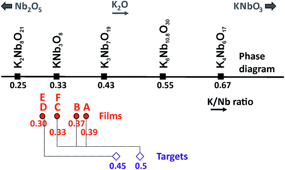 | ||
| Fig. 1 Scheme displaying the K/Nb ratio in samples A to F, relatively to the K/Nb ratio of the targets used to synthesize these samples, and relatively to the K/Nb ratio of the known niobates of the Nb2O5–KNbO3 phase diagram. | ||
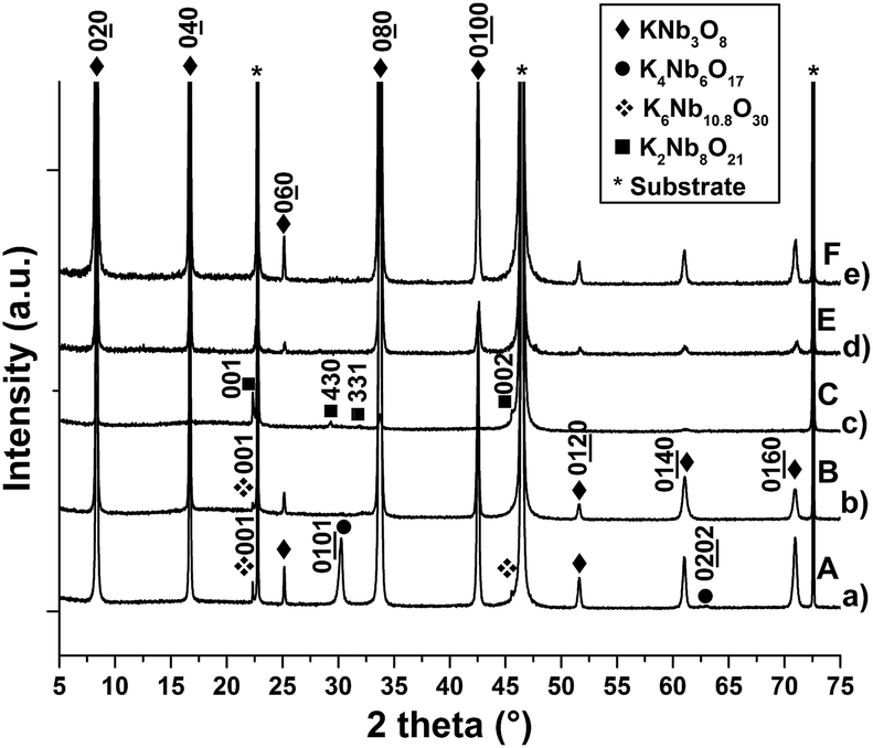 | ||
| Fig. 2 XRD diagrams in θ/2θ mode of KNb3O8 thin films, with or without other phases, grown on (100)STO by PLD with various elaboration parameters (cf. Table 2): (a) film A, (b) film B, (c) film C, (d) film E, (e) film F (substrate: *). | ||
Thus, the amount of potassium in this film is too high for the targeted compound. It is surprising to observe the growth of the K4Nb6O17 phase since the composition of the film if far from that of this compound. Actually, we have observed that this phase has the ability to grow in a very large composition range.52 To decrease the amount of potassium relatively to that of Nb, a film was synthesized with a higher target–substrate distance (DTS = 55 mm, film B, Fig. 2b). Film B is mainly constituted of the KNb3O8 phase. Displaying the intensity of the diagram in logarithmic scale allows to observe a peak located at 2θ = 22.31° (d = 3.98 Å), the intensity of which is 160 counts per s while that of the (020)KNb3O8 peak is 88![[thin space (1/6-em)]](https://www.rsc.org/images/entities/char_2009.gif) 500 counts per s. This peak corresponds to the (001)K6Nb10.88O30 TTB phase, which is therefore still present. From this configuration, additional increase of DTS (Fig. 2c, film C) leads to a depletion of potassium in the film and to the growth of the K2Nb8O21 niobate.51,53 Using a target with a lower K amount (films D and E, target K0.45NbO2.5, DTS = 70 mm) also leads to the growth of the KNb3O8 phase together with a small amount of K2Nb8O21 (Fig. 2d and SI1†). For these two films, the presence of K2Nb8O21 is not observed in the XRD diagrams but is evidenced by SEM micrographs (see below). Finally, pure KNb3O8 films were obtained from the same target of composition K0.45NbO2.5 with a lower target–substrate distance (DTS = 55 mm, film F, Fig. 2e). SEM micrographs display that the microstructure of KNb3O8 on STO, for all samples synthesized with a fluence fixed at 1.85 J cm−2 (films A–D), is made of elongated and parallelepiped-shaped crystals of dimensions 500 nm in length, and 50–75 nm in width (Fig. 3a–c and SI2 ESI†). Two variants of elongated crystals are observed, corresponding to two in-plane orientations (marked by blue arrows in Fig. 3b), one growing parallel to the [010]STO direction, and the other one at 90° in regards to the first variant.
500 counts per s. This peak corresponds to the (001)K6Nb10.88O30 TTB phase, which is therefore still present. From this configuration, additional increase of DTS (Fig. 2c, film C) leads to a depletion of potassium in the film and to the growth of the K2Nb8O21 niobate.51,53 Using a target with a lower K amount (films D and E, target K0.45NbO2.5, DTS = 70 mm) also leads to the growth of the KNb3O8 phase together with a small amount of K2Nb8O21 (Fig. 2d and SI1†). For these two films, the presence of K2Nb8O21 is not observed in the XRD diagrams but is evidenced by SEM micrographs (see below). Finally, pure KNb3O8 films were obtained from the same target of composition K0.45NbO2.5 with a lower target–substrate distance (DTS = 55 mm, film F, Fig. 2e). SEM micrographs display that the microstructure of KNb3O8 on STO, for all samples synthesized with a fluence fixed at 1.85 J cm−2 (films A–D), is made of elongated and parallelepiped-shaped crystals of dimensions 500 nm in length, and 50–75 nm in width (Fig. 3a–c and SI2 ESI†). Two variants of elongated crystals are observed, corresponding to two in-plane orientations (marked by blue arrows in Fig. 3b), one growing parallel to the [010]STO direction, and the other one at 90° in regards to the first variant.
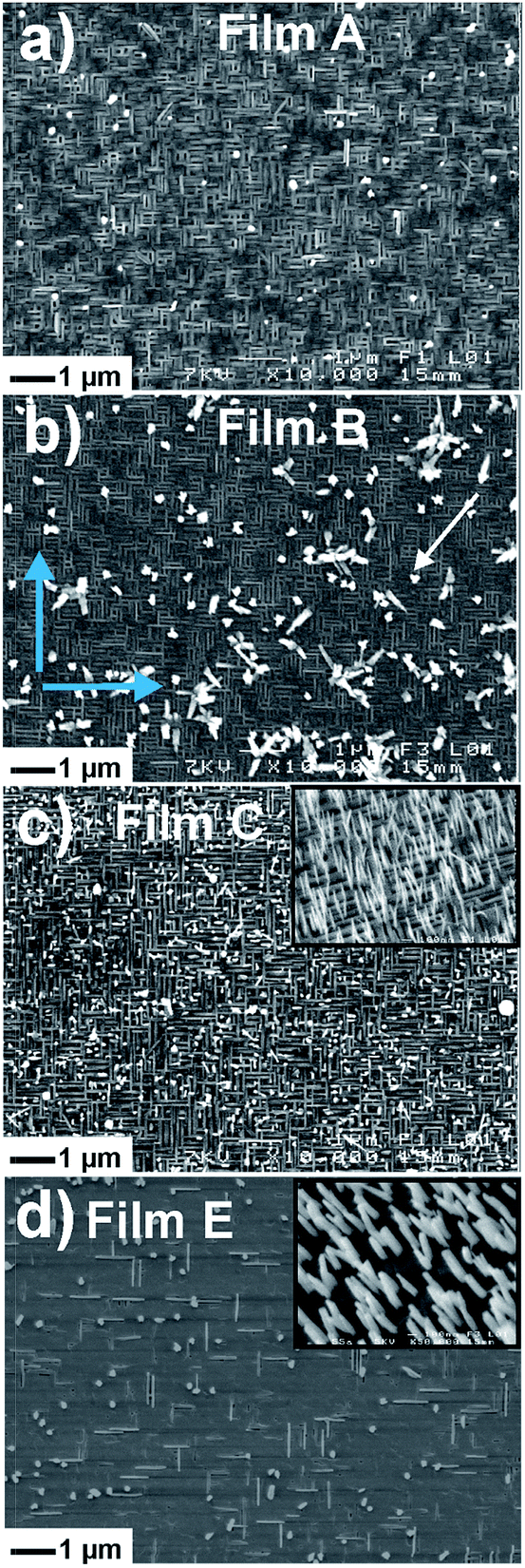 | ||
| Fig. 3 SEM micrographs of the KNb3O8 thin films, denoted A (a), B (b), C (c), E (d) in text and Table 2, grown on (100)STO. The blue arrows in (b) show the two in-plane elongation directions of the KNb3O8 crystals growing at 90° from each other. The insets in (c) and (d) are SEM micrographs of the films C and E tilted at 45° showing the growth of vertical ribbons and rods. | ||
The samples made at fluence of 1.95 J cm−2 (films E and F) have a different morphology. Indeed, they are constituted of macroscopic flat lamellas that are irregular in shape but higher in dimensions (0.5–1 μm) (Fig. 3d). It has been reported that when the fluence is higher, the kinetic energies of ablated species are increased. As a consequence, the fluence is known to affect the growth mode of the film, that follows either the Volmer-Weber mode, with islands formation, (3 dimensions (3D) growth), or Frank–van der Merwe mode (layer-to-layer formation, 2D) or Stranski–Krastanov mode (2D + 3D).54,55 In the present case, the microstructures displayed in Fig. 3a–c would correspond to the first growth mode, and the morphology of the parallelepiped crystals reflects the anisotropy of the crystal structure. Madaro et al.35 have synthesized KNb3O8 plate-like crystals by molten salt synthesis and shown that morphology of crystals depends both of temperature and salt/oxide weight ratio. They have evidenced that the plates have the [010]-preferential orientation and that the length of the plates grows along the [001] direction. They suggested that this direction which corresponds to the lower connectivity between the corner-sharing NbO6-octahedra, is perpendicular to the facets with lower surface energy. Indeed, the particle shape is thermodynamically controlled by the Wulff construction which is the surface that minimizes the total surface free energy of a crystal, as a function of crystallographic orientation.56 Therefore, crystals with anisotropic crystalline structure have generally an anisotropic shape.57 In the case of flat lamellas (films E and F), the growth mode would follow the Frank–van der Merwe mode and the anisotropy of the crystal dimensions is also present, but the films being very flat, the SEM contrast is very low and limits the observation. The thicknesses of the films B and E are about 205–215 nm and 120–135 nm, respectively (Fig. SI3 ESI†).
3.2. Transmission electron microscopy characterization
As shown above, depending on the fluence as a unique parameter, two types of films were observed, differing strongly in their morphology. Also, SEM photographs show some outgrowths perpendicular to the film surface. TEM was used to characterize these features. | ||
| Fig. 4 (a) BF micrograph of some KNb3O8 crystals of the film D; the blue arrow shows the elongation direction of the crystals. (b) Corresponding EDP along the [010] zone axis. Dashed lines show diffusive lines present in the pattern, that can be better seen in the inset. (c) DF micrograph of KNb3O8 crystals obtained by selecting the KNb3O8 (100) reflection labeled by a white arrow in the EDP in the inset. (d) DF micrograph of the same crystals obtained by selecting a diffuse line labeled by a white arrow in the EDP in the inset. (e) BF micrograph of KNb3O8 crystals of the film E. (f) Corresponding EDP along the [010] zone axis. | ||
Electron diffraction experiments (Fig. 5b), performed on 10 different nanoribbons and 10 different nanorods, have evidenced that these nanoribbons and nanorods are actually made of the K2Nb8O21 phase, with the [001] direction parallel to elongation direction (Fig. 5a), that corresponds to the peak located at 2θ = 22.42° (d = 3.96 Å) in the XRD pattern (Fig. 2c). Most of these nanoobjects present structural disorder along (001) planes, as evidenced by diffusion lines in the electron diffraction pattern (Fig. 5b). These results are in agreement with the work of Xu et al. who have synthesized nanoribbons and nanorods of this phase by a molten salt route.60,61 Recently, Paria Sena et al. have solved the crystalline structure of the K2Nb8O21 phase in the K–Nb–Ta–O system, and demonstrated that this structure is a pseudo-superstructure of the TTB phase, with the following lattice parameters a ∼ 2√2 aTTB ∼ 37.4 Å, b ∼ bTTB, and c ∼ cTTB.53 Therefore, both TTB phase and its superstructure have the same growth behavior, i.e. very anisotropic crystal growth with their [001] out-of-plane growth direction corresponding to their elongation direction. Accurate study of the growth of TTB nanorods and of K2Nb8O21 nanoribbons will be the subject of another article.52
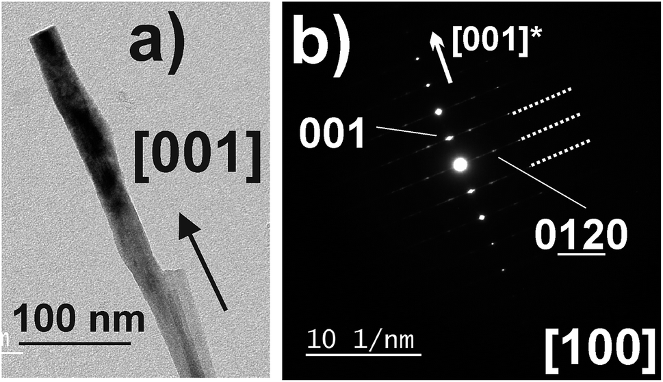 | ||
| Fig. 5 (a) BF micrograph of a K2Nb8O21 vertical ribbon. (b) Corresponding EDP along the [100] zone axis. Dashed lines show diffusive lines present in the pattern. | ||
3.3. Epitaxy of KNb3O8 thin films
Fig. 6a shows the results of the epitaxy study of the (010) oriented KNb3O8 phase on (100)STO (film B). Same results were obtained for film E (Fig. SI4 ESI†). The φ-scan performed on the {240} planes of the KNb3O8 phase shows 4 peaks separated by 90°, located at the same azimuths that the characteristic peaks of the {110} planes of the STO substrate. As KNb3O8 is orthorhombic, these 4 peaks correspond to two in-plane orientation families, the first of it diffracts at 0° and 180°, and the second one at −90° and 90°. This result is consistent with the observation of two types of crystallites elongated along 2 perpendicular directions (Fig. 3a). The coincidence between the lattice of STO and that of KNb3O8 is illustrated on the Fig. 6b: the two variants are oriented relatively to the substrate, and the coincidences between the c parameter of each of them with the c and b parameters of STO are schemed by red (variant 1) and blue (variant 2) segments. This epitaxy is governed by the following relationships,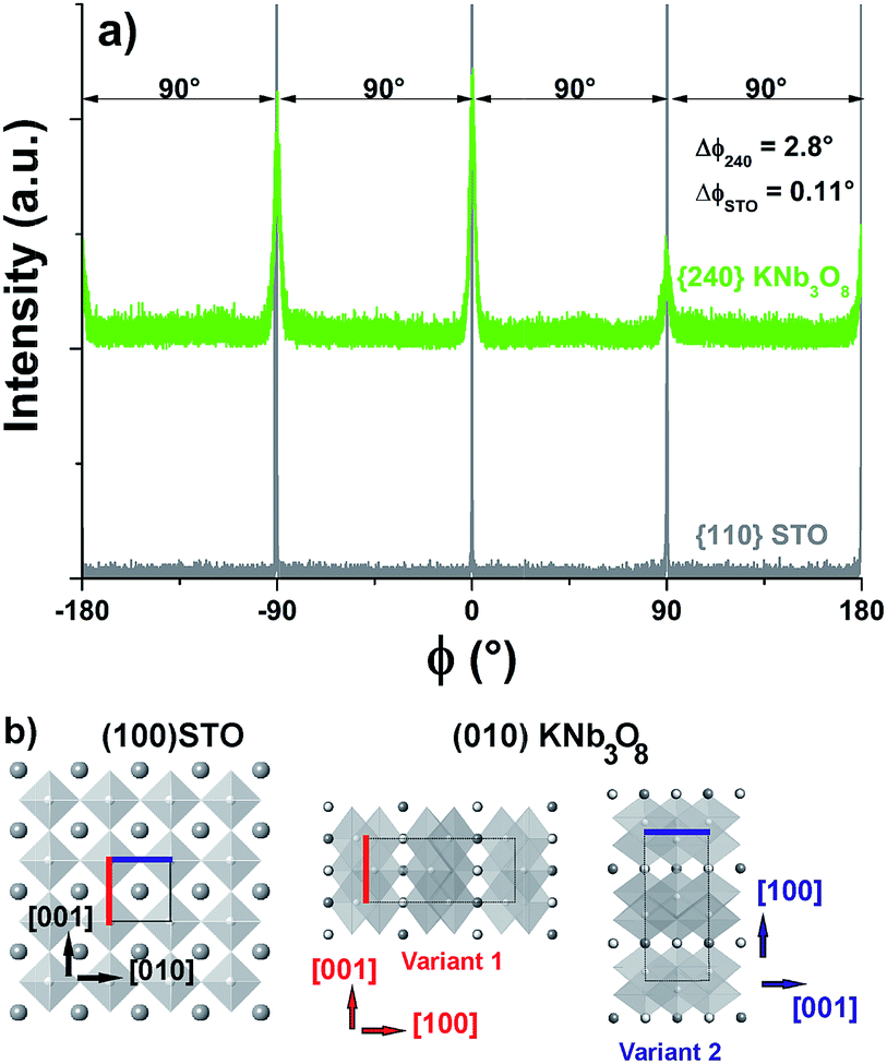 | ||
| Fig. 6 (a) φ-Scans of the {240} planes of the KNb3O8 phase (green line) and of the {110} planes of the (100)STO substrate (grey line) (film B). (b) Scheme of (100)STO substrate and of the two corresponding orientations of KNb3O8 crystals on (100)STO (view along the normal to the substrate, i.e. along the [010] direction of STO, and along the [010] direction of the KNb3O8 phase). The variant 1 is clamped on the substrate in reason of the low mismatch between its c edge relatively to that of the c edge of STO (red segments). The same phenomena is observed for variant 2 (c edge close to b edge of STO, blue segments). | ||
for variant 1:
(010)KNb3O8//(100)STO
[001]KNb3O8//[001]STO
[100]KNb3O8//[010]STO
and for variant 2:
(010)KNb3O8//(100)STO
[001]KNb3O8//[010]STO
[100]KNb3O8//[001]STO
Epitaxial growth is due on one hand to the low mismatch between the lattice parameter of the substrate and the c parameter of KNb3O8 ((aSTO − cKNb3O8)/aSTO × 100 = 2.7%), and on the other hand, to the low mismatch between 9 lattice units of the substrate and 4 lattice units of the film along the second parameter ((9aSTO − 4aKNb3O8)/(9aSTO) = −1.33%). This last relationships belongs to the frame of the domain matching epitaxy, in which m lattice units of the film match with p lattice units of the substrate. The values of m and p are defined as the minimum integers which satisfy the relation: m dKNb3O8 = p dSTO, dKNb3O8 and dSTO being the respective atomic distances in the film and substrate parallel directions.62,63
The rocking-curve (ω-scan) around the 020 reflection of KNb3O8 reveals a medium value of the mosaicity (Δω = 1.1° for film B, and 1.85° for film E, whereas for STO Δω = 0.034°; Fig.SI5 ESI†) showing some misorientation of this phase on the substrate.
It is probable that the growth of KNb3O8 on polycrystalline or amorphous substrates will lead to the [010] preferential orientation as well, as for other lamellar phases with large interlamellar distance,64 but with no-ordering in the plane. Therefore, the ability of KNb3O8 to grow with an in-plane orientation on a single-crystalline substrate is interesting to increase properties compared to those of textured films.
3.4. Exchange properties
Hosogi et al. have shown that the exchanged layered Sn2+/K4Nb6O17 niobate had visible-range light absorption bands leading to photocatalytic properties under visible light, with a reduction of the energy gap from 3.5 to 2.8 eV.65 From these results, we studied the ability to exchange K+ by Sn2+ in KNb3O8 films. Fig. 7 displays XRD patterns of the film F before protonation (Fig. 7a), after protonation (Fig. 7b and c) and after exchange experiments (Fig. 7d). After a day in nitric acid, the XRD peaks of the film F2 are noticeably shifted to lower angle values and splitted in 3 contributions, labelled by H, H′ and H′′ in Fig. 7b. After a few hours in a desiccator, the film was re-examined by XRD, and in the resulting XRD pattern (Fig. 7c), both H′ and H′′ peaks have vanished or almost vanished while the intensity of the peaks H was considerably increased. The shift of the 020 peak corresponds to an increase of the intereticular distance d020 from 10.59 to 11.23 Å, therefore to an increase of the interlamellar spacing from 21.18 to 22.46 Å. This increase is due to the larger size of the H3O+ ion (280 pm, hydrated value) compared to that of the K+ ion (152 pm). This result is in full agreement with what was observed for a KNb3O8 powder after being exchanged in acid nitric to form the H3ONb3O8 phase (see Table 1) with an increase of the lattice parameter b to the value 22.47 Å.12,32,42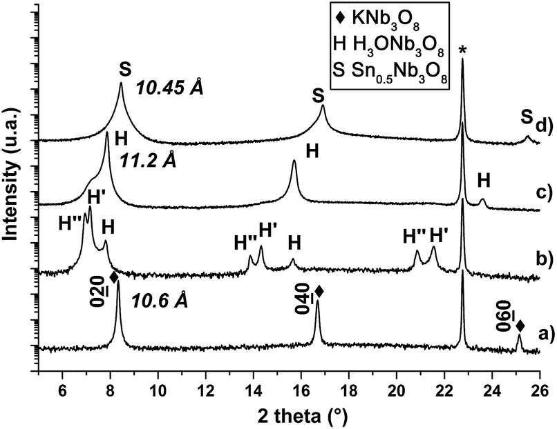 | ||
| Fig. 7 XRD diagrams in θ/2θ mode: (a) KNb3O8 film (film F); (b) same film (F2) after 24 h in a HNO3 solution (6 N); (c) same film (F3) after 8 h in air in a desiccator; (d) same film after 64 h in a SnCl2/HCl solution (substrate: *). | ||
The presence of H′ and H′′ peaks is most likely due to the intercalation of some species that have induced swelling of the lattice, characterized by an increase of the lattice parameter b to 24.68 Å (d020 = 12.34 Å) and 25.44 Å (d020 = 12.72 Å), respectively. The vanishing of these H′ and H′′ peaks after the stay of the sample in anhydrous atmosphere for a few hours suggests that these intercalated species are probably water and/or hydrated hydronium ions, as proposed by Takahashi et al. that have observed the same phenomena after the protonation of KTiNbO5 niobate.66 We performed infra-red spectrometry on a H3ONb3O8 film, just after protonation, and after few hours in a desiccator (Fig. SI6 ESI†). Some absorptions bands observed in the spectrum of the just-protonated film are not present for the dehydrated film, as it was reported for other crystalline hydrates, and attributed to water and/or hydrated hydronium ions.67,68 After dehydration, more matter intercalated with H3O+ ions is afterwards diffracting, involving the increase of the peak H intensity in XRD diagram. The film F2 was analysed by TEM-EDXS and found to be fully free of potassium, demonstrating the total exchange of the potassium ions by the hydronium ions (Fig. SI7 ESI†). From TEM, the lattice parameters were measured as being a = 9.1 Å and c = 3.84 Å (Fig. SI8 ESI†). Fig. 7d shows the XRD pattern of the H3ONb3O8 film subsequently immersed 64 h in a tin chloride solution (film F3). The evolution of the XRD patterns of this film was checked daily and was no longer modified after 3 days in the solution. It is observed that the 020 peak shifts now to a higher angle value, corresponding to a decrease of the intereticular distance from 11.23 Å (b = 22.46 Å) to 10.45 Å (b = 20.9 Å). This results corresponds to the decrease of the radius of the intercalated ion (83 pm for Sn2+) relatively to that of H3O+. The Fig. 8a shows the EDP of a part of the film after the two exchange reactions, corresponding to the diffraction of several crystals. By using a smaller selected area aperture, contribution of both variants are separated in Fig. 8b and c. These patterns are close to that displayed in Fig. 4f, with the lattice parameters a = 9.23 Å and c = 3.93 Å that are slightly higher than the values of the parent phase H3ONb3O8, and show that the crystallinity of the phase was preserved. DF micrographs taken by selecting a reflection for each variant (Fig. 8d and e) show that the microstructure built from of rectangular lamellas growing at 90° from each other is also preserved. The Fig. SI7 ESI† shows the TEM-EDXS spectra of film F3 compared to that of the films KNb3O8 and H3ONb3O8, demonstrating the complete exchange of K+ by Sn2+. The composition measured by TEM-EDXS is about Sn0.6Nb3Ox, therefore close to what is expected for a complete exchange with respect of electroneutrality. These two exchange reactions were carried out at room temperature, without stirring and in a relative short time, relatively to other exchange reactions performed on powder that take 2–3 days for protonation6,12,19 and several days for exchange.12,23
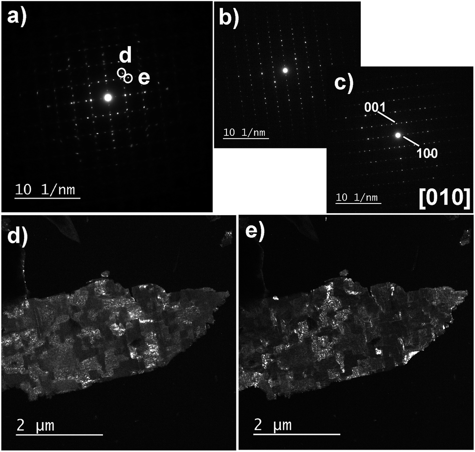 | ||
| Fig. 8 (a) EDP of a part of the film F3, i.e. film F after protonation and intercalation. (b and c) EDPs registered in the same area with a smaller SAED aperture, showing [010] zone axis of two SnNb3O8 crystals oriented at 90° from each other. (d and e) DF micrographs obtained by selecting the {401} reflections labeled by the letters (d) and (e) in Fig. 8a. | ||
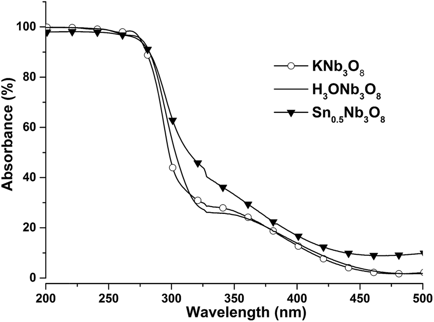
Fig. SI9 ESI† shows that the thin film grown on silica with the same deposition parameters than the film F grown on STO is a single-phase (010)KNb3O8 film. As emphasized above, the film is (010) preferentially oriented even if the substrate is amorphous. This film was successfully protonated before exchange of the potassium ions for the tin ions as shown in Fig. SI9 ESI.† In order to determine if crystal damage results from the exchange, we have performed high resolution transmission electron microscopy (HRTEM) on the KNb3O8 film, and on the SnNb3O8 film (Fig. SI10 ESI†). The micrographs and their fast Fourier transforms show that the SnNb3O8 film does not present crystal damage. Fig. 9 shows the absorbance spectra of the KNb3O8 thin film grown on silica, before and after protonation, and after exchange. The spectra of the H3ONb3O8 and Sn0.5Nb3O8 films are red-shifted relatively to that of the KNb3O8 film towards the visible range. The corresponding energy gaps were estimated to be 3.9 eV for KNb3O8 film (for 3.7 eV for powder),6 3.78 eV for H3ONb3O8 film, and 3.57 eV for Sn0.5Nb3O8 film. The effect of Sn exchange on the oxide band gap value was previously studied for the other layered potassium niobate in this system, i.e. K4Nb6O17 compound, by Hosogi et al.65 These authors reported that the Sn2+/K4Nb6O17 gap was 0.7 eV narrower than that of K4Nb6O17, while in the present work, Sn0.5Nb3O8 film gap was narrower of only 0.33 eV. Nevertheless, these first results are promising for synthesis of exchange-Nb3O8 films with visible-range activity. According to the large amount of species that were intercalated in KNb3O8 powder in the past, the present results are also promising for formation of new intercalated KNb3O8 thin films for numerous applications as catalysis, electrochemistry, depollution of waste water, etc. In addition, lamellar-shaped films are expected to show better photocatalytic properties than the rod-shaped films. Indeed, the effect of the shape of powder KNb3O8 and HNb3O8 crystals on photocatalytic properties was recently studied by Li et al. and Liu et al.6,10 Both groups found that belt shaped crystals present higher photocatalytic properties than the rod-like crystals.
 | ||
| Fig. 9 Absorbance spectra of KNb3O8, H3ONb3O8 and Sn0.5Nb3O8 films. | ||
4. Conclusions
Thin films of epitaxially grown KNb3O8 phase were synthesized by PLD, with the ability to change the morphology of the crystals constituting the film, from parallelepiped-shaped rods to thin lamellas, by changing the laser fluence. The rods are actually built from alternated slabs of KNb3O8 phase and of a poorly crystallized K2Nb8O21 phase. On the contrary, the lamellas are single phased and well-crystallized and present larger dimensions. We believe that this lamellar morphology of the film would be benefit on the properties as it was observed in the past for KNb3O8 crystals synthesized by molten salt method. The ability to exchange K+ by H3O+ and then Sn2+ was observed for KNb3O8 films, leading to potential properties based on intercalation of various species in the Nb3O8− matrix as it was reported for powder. Perspectives of this work is to study these intercalation properties on cheaper polycrystalline and amorphous substrates, and also by low temperature deposition methods as chemical solution deposition.Acknowledgements
The authors are grateful to F. Gouttefangeas, L. Joanny, J. Le Lannic, and I. Péron from CMEBA facility (ScanMAT, University of Rennes 1) for the assistance in SEM observations and SEM-EDXS analyses, and to Pr. Olivier Guillou for the access to IR spectrometer. TEM was performed on THEMIS platform (ScanMAT, University of Rennes 1). The RBS experiments were performed under the convention for SAFIR@ALTAÏS between the Université Pierre et Marie Curie and the University of Namur. Dr A. Perrin is warmly acknowledged for the fruitful discussions. ScanMAT (CMEBA, THEMIS) thanks Région Bretagne, Rennes Métropole and European Union for financial support (CPER-FEDER 2007–2014). VD acknowledges the Région Bretagne, Rennes Métropole and CNRS for their financial supports.References
- G. Centi and S. Perathoner, Workshop Innov. Appl. Layer. Mater. Catal. Nanotechnol., Microporous Mesoporous Mater., 2008, 107, 3–15 CrossRef CAS.
- V. Nicolosi, M. Chhowalla, M. G. Kanatzidis, M. S. Strano and J. N. Coleman, Science, 2013, 340, 1226419 CrossRef.
- M. H. Han, E. Gonzalo, G. Singh and T. Rojo, Energy Environ. Sci., 2015, 8, 81–102 CAS.
- R. Ma and T. Sasaki, Acc. Chem. Res., 2015, 48, 136–143 CrossRef CAS PubMed.
- M. Gasperin, Acta Crystallogr., Sect. B: Struct. Crystallogr. Cryst. Chem., 1982, 38, 2024–2026 CrossRef.
- X. Li, H. Pan, W. Li and Z. Zhuang, Appl. Catal., A, 2012, 413–414, 103–108 CAS.
- G. Blasse and F. Vantol, Solid State Commun., 1995, 95, 465–468 CrossRef CAS.
- X. Kong, D. Hu, P. Wen, T. Ishii, Y. Tanaka and Q. Feng, Dalton Trans., 2013, 42, 7699–7709 RSC.
- G. Zhang, J. Gong, X. Zou, F. He, H. Zhang, Q. Zhang, Y. Liu, X. Yang and B. Hu, Chem. Eng. J., 2006, 123, 59–64 CrossRef CAS.
- X. Liu, W. Que and L. B. Kong, J. Alloys Compd., 2015, 627, 117–122 CrossRef CAS.
- Z. J. Yang, Y. F. Li, Q. B. Wu, N. Ren, Y. H. Zhang, Z. P. Liu and Y. Tang, J. Catal., 2011, 280, 247–254 CrossRef CAS.
- R. Nedjar, M. Borel and B. Raveau, Mater. Res. Bull., 1985, 20, 1291–1296 CrossRef CAS.
- A. S. Dias, S. Lima, D. Carriazo, V. Rives, M. Pillinger and A. A. Valente, J. Catal., 2006, 244, 230–237 CrossRef CAS.
- A. Takagaki, C. Tagusagawa, S. Hayashi, M. Hara and K. Domen, Energy Environ. Sci., 2010, 3, 82–93 CAS.
- S. Masud, M. Zarei, M. L. Lopez, J. Gardea-Torresdey, C. V. Ramana and G. B. Saupe, Mater. Sci. Eng., B, 2010, 174, 66–70 CrossRef CAS.
- T. Shibata, G. Takanashi, T. Nakamura, K. Fukuda, Y. Ebina and T. Sasaki, Energy Environ. Sci., 2011, 4, 535–542 CAS.
- M. Zarei-Chaleshtori, M. Hosseini, R. Edalatpour, S. M. S. Masud and R. R. Chianelli, Microchem. J., 2013, 110, 361–368 CrossRef CAS.
- P. Zhou, Q. Li, J. He, D. Li and Z. Li, Russ. J. Phys. Chem. A, 2015, 89, 2097–2104 CrossRef CAS.
- N. Lee and Y.-M. Chung, Appl. Surf. Sci., 2016, 370, 160–168 CrossRef CAS.
- S. Liang, L. Wen, S. Lin, J. Bi, P. Feng, X. Fu and L. Wu, Angew. Chem., 2014, 126, 2995–2999 CrossRef.
- X. Wang, W. Hou, H. Wang and Q. Yan, Catal. Commun., 2002, 3, 275–280 CrossRef CAS.
- N. Belmokhtar, R. Brahimi, R. Nedjar and M. Trari, Mater. Sci. Semicond. Process., 2015, 39, 433–440 CrossRef CAS.
- V. R. L. Constantino, M. A. Bizeto and H. F. Brito, J. Alloys Compd., 1998, 278, 142–148 CrossRef CAS.
- T. Nakato, K. Kuroda and C. Kato, Chem. Mater., 1992, 4, 128–132 CrossRef CAS.
- S. Wang, C. Liu, L. Liu, X. Zhang, J. Gong and Z. Tong, Synth. React. Inorg., Met.-Org., Nano-Met. Chem., 2012, 42, 251–255 CrossRef CAS.
- R. Nedjar, M. Borel and B. Raveau, Z. Anorg. Allg. Chem., 1986, 541, 198–204 CrossRef.
- R. Nedjar, M. Borel and B. Raveau, J. Solid State Chem., 1987, 71, 451–457 CrossRef CAS.
- M. A. Bizeto, D. L. A. De Faria and V. R. L. Constantino, J. Mater. Sci. Lett., 1999, 18, 643–646 CrossRef CAS.
- X. Zhang, L. Liu, J. Ma, X. Yang, X. Xu and Z. Tong, Mater. Lett., 2013, 95, 21–24 CrossRef CAS.
- H. Pan, X. Li, Z. Zhuang and C. Zhang, J. Mol. Catal. A: Chem., 2011, 345, 90–95 CrossRef CAS.
- X. Li, H. Pan, Q. Hu and C. Zhang, J. Alloys Compd., 2011, 509, 6252–6256 CrossRef CAS.
- X. Liu, W. Que, Y. Xing, X. Yin, Y. He and H. M. A. Javed, J. Cryst. Growth, 2015, 419, 149–152 CrossRef CAS.
- H. Nakayama, M. Nose, S. Nakanishi and H. Iba, J. Power Sources, 2015, 287, 158–163 CrossRef CAS.
- K. Nassau, J. Shiever and J. L. Bernstein, J. Electrochem. Soc., 1969, 116, 348–353 CrossRef CAS.
- F. Madaro, R. Saeterli, J. R. Tolchard, M.-A. Einarsrud, R. Holmestad and T. Grande, CrystEngComm, 2011, 13, 1304–1313 RSC.
- S. Suzuki, K. Teshima, A. Yamaguchi, K. Yubuta, T. Shishido and S. Oishi, CrystEngComm, 2012, 14, 987–992 RSC.
- G. Zhang, F. He, X. Zou, J. Gong, H. Tu, H. Zhang, Q. Zhang and Y. Liu, J. Alloys Compd., 2007, 427, 82–86 CrossRef CAS.
- T. M. Duarte, L. M. C. Honorio, A. S. Brito, J. K. D. Souza, E. Longo, R. L. Tranquilin, A. G. Souza, I. M. G. Santos and A. S. Maia, in Brazil Mrs Meeting 2014, 2015, vol. 97, p. 012001 Search PubMed.
- C. M. Papa, A. J. Cesnik, T. C. Evans and K.-S. Choi, Langmuir, 2015, 31, 9502–9510 CrossRef CAS PubMed.
- J. F. Liu, X. L. Li and Y. D. Li, J. Cryst. Growth, 2003, 247, 419–424 CrossRef CAS.
- Z. Y. Zhan, C. Y. Xu, L. Zhen, W. S. Wang and W. Z. Shao, Ceram. Int., 2010, 36, 679–682 CrossRef CAS.
- L. Li, J. Deng, J. Chen, X. Sun, R. Yu, G. Liu and X. Xing, Chem. Mater., 2009, 21, 1207–1213 CrossRef CAS.
- L. Li, J. Deng, R. Yu, J. Chen, X. Wang and X. Xing, Inorg. Chem., 2010, 49, 1397–1403 CrossRef CAS PubMed.
- B. Gao, J. Fu, K. Huo, W. Zhang, Y. Xie and P. K. Chu, J. Am. Ceram. Soc., 2011, 94, 2330–2338 CrossRef CAS.
- A. Rousseau, V. Laur, M. Guilloux-Viry, G. Tanné, F. Huret, S. Députier, A. Perrin, F. Lalu and P. Laurent, Thin Solid Films, 2006, 515, 2353–2360 CrossRef CAS.
- C. Maréchal, E. Lacaze, W. Seiler and J. Perriére, Phys. C, 1998, 294, 23–32 CrossRef.
- E. Irle, R. Blachnik and B. Gather, Thermochim. Acta, 1991, 179, 157–169 CrossRef CAS.
- M. Gasperin and M. Le Bihan, J. Solid State Chem., 1982, 43, 346–353 CrossRef CAS.
- G. Fallon, B. Gatehouse and L. Guddat, J. Solid State Chem., 1986, 61, 181–187 CrossRef CAS.
- N. Kumada and N. Kinomura, Eur. J. Solid State Inorg. Chem., 1997, 34, 65–72 CAS.
- P. Appendino, M. Montorsi and M. Vallino, Ann. Chim., 1976, 66, 417–427 CAS.
- A. Waroquet, PhD Thesis Dissertation, Université de Rennes 1, 2015.
- R. Paria Sena, A. A. Babaryk, S. Khainakov, S. Garcia-Granda, N. S. Slobodyanik, G. Van Tendeloo, A. M. Abakumov and J. Hadermann, Dalton Trans., 2016, 45, 973–979 RSC.
- H. Fujioka, in Handbook of Crystal Growth, North-Holland, Boston, 2nd edn, 2015, pp. 365–397 Search PubMed.
- C. Xu, S. Wicklein, A. Sambri, S. Amoruso, M. Moors and R. Dittmann, J. Phys. D: Appl. Phys., 2014, 47, 034009 CrossRef.
- G. Wulff, Z. Kristallogr. - Cryst. Mater., 2015, 34, 449 Search PubMed.
- Handbook of crystal growth, G. Dhanaraj, K. Byrappa, V. Prasad and M. Dudley, Springer Berlin Heidelberg, Berlin, Heidelberg, 2010 Search PubMed.
- Q. Simon, V. Dorcet, P. Boullay, V. Demange, S. Députier, V. Bouquet and M. Guilloux-Viry, Chem. Mater., 2013, 25, 2793–2802 CrossRef CAS.
- M. Lundberg and M. Sundberg, J. Solid State Chem., 1986, 63, 216–230 CrossRef CAS.
- C.-Y. Xu, L. Zhen, L. Yang, K. He, W.-Z. Shao and L.-C. Qin, Ceram. Int., 2008, 34, 435–437 CrossRef CAS.
- C.-Y. Xu, L. Zhen, R. Yang and Z. L. Wang, J. Am. Chem. Soc., 2007, 129, 15444–15445 CrossRef CAS PubMed.
- J. Narayan, K. Dovidenko, A. K. Sharma and S. Oktyabrsky, J. Appl. Phys., 1998, 84, 2597–2601 CrossRef CAS.
- M. Nistor, N. B. Mandache, J. Perrière, C. Hebert, F. Gherendi and W. Seiler, Thin Solid Films, 2011, 519, 3959–3964 CrossRef CAS.
- R. Abe, M. Hara, J. N. Kondo, K. Domen, K. Shinohara and A. Tanaka, Chem. Mater., 1998, 10, 1647–1651 CrossRef CAS.
- Y. Hosogi, H. Kato and A. Kudo, J. Phys. Chem. C, 2008, 112, 17678–17682 CAS.
- H. Takahashi, M. Kakihana, Y. Yamashita, K. Yoshida, S. Ikeda, M. Hara and K. Domen, Phys. Chem. Chem. Phys., 2000, 2, 4461–4464 RSC.
- A. S. Gilbert and N. Sheppard, J. Chem. Soc. D, 1971, 337–338 RSC.
- M. Hashimoto, G. Koyano and N. Mizuno, J. Phys. Chem. B, 2004, 108, 12368–12374 CrossRef CAS.
Footnote |
| † Electronic supplementary information (ESI) available: RBS spectrum of KNb3O8 film on sapphire; XRD, SEM (film D); cross-sectional SEM (films B and D); phi-scan (film E); rocking-curves (films B and E); IR spectra (film F2); EDXS spectra (films F, F2, F3); brightfield micrograph and electron diffraction pattern (film F2); XRD of KNb3O8 film on SiO2; HRTEM (films F, F2). See DOI: 10.1039/c7ra00261k |
| This journal is © The Royal Society of Chemistry 2017 |