
 Open Access Article
 This Open Access Article is licensed under a
 Creative Commons Attribution 3.0 Unported Licence
Resistive switching and related magnetization switching in Pt/BiFeO3/Nb:SrTiO3 heterostructures
Meng Zhaoab,
Yongdan Zhu†
 *ab,
Yuan Zhanga,
Tingting Zhanga,
Da Qiua,
Guohong Laia,
Cheng Hua,
Qiangwen Wangb,
Feng Zhangb and
Meiya Li*b
*ab,
Yuan Zhanga,
Tingting Zhanga,
Da Qiua,
Guohong Laia,
Cheng Hua,
Qiangwen Wangb,
Feng Zhangb and
Meiya Li*b
aSchool of Information Engineer, Hubei University for Nationalities, Enshi, 445000, Hubei, P. R. China
bSchool of Physics and Technology, Key Laboratory of Artificial Micro/Nano Structures of the Ministry of Education, Wuhan University, Wuhan 430072, P. R. China. E-mail: yongdan_zhu@whu.edu.cn; myli@whu.edu.cn
First published on 27th April 2017
Abstract
BiFeO3 (BFO) thin films were epitaxially grown on a 0.7 wt% Nb-doped (001) SrTiO3 (NSTO) single-crystal substrate by pulsed laser deposition to form a Pt/BFO/NSTO heterostructure. This heterostructure exhibits stable bipolar resistive switching behavior with a maximum Roff/Ron ratio of 105, well retention and multilevel memory properties. Meanwhile, the saturation magnetization (Ms) of BFO film shows reversible switching upon different resistance states. The BFO film shows high saturation magnetization at a high resistance state, while it shows low saturation magnetization at a low resistance state. These resistive and magnetization switching properties are attributed to the modulation effect of the ferroelectric polarization reversal on the width of depletion region and the height of potential barrier via the charge trapping and detrapping process combined with the migration of oxygen vacancies at the BFO/NSTO interface. This study demonstrates that Pt/BFO/NSTO heterostructure has potential application in nonvolatile resistive switching memory and novel magnetoelectric coupling devices.
1. Introduction
Recently, nonvolatile resistive switching (RS) effects have attracted considerable attention due to their possible applications in the next generation of resistance random access memory with high speed, high density and low power consumption.1–3 Up to now, the resistive switching effect has been widely observed in several kinds of materials such as ferroelectric materials, magnetic materials and photoelectric materials.4–15 It has also been found that some other physical parameters could be changed simultaneously during the resistive switching process, which provides us with a promising method to design multifunctional devices. For instance, the electrical manipulation of room temperature ferromagnetism and resistive switching were observed in many thin films such as TiO2,6 ZnO,7,15 NiO,8–10 CFO11 and BFO,13 which is likely to be a powerful supplement to the magnetoelectric coupling effect. Various models, such as formation and rupture of conductive filaments, oxygen vacancy migration and charge trapping/detrapping, have been proposed for the origin of RS and magnetization switching, but the understanding of resistive and magnetization switching is still under debate due to the diversity of materials and preparation methods.4–15 Therefore, the correlation and modulation between RS and magnetism switching is one of the important issues to be studied at present.BFO has been widely investigated as a promising multiferroic material because of the coexistence of ferroelectricity and magnetism, which shows potential applications in multifunctional devices.16–18 The research of BFO has been carried out in our previous studies, in which the BFO films with good ferroelectricity have been prepared successfully through pulsed laser deposition method.12,19–21 Recently, BFO is also found to exhibit various RS behaviors due to different device structure and preparation process, which has attracted significant attention. The unipolar, bipolar and nonpolar RS behaviors have been found in the epitaxial and polycrystalline thin films even in the nano-islands and nanocapacitor arrays device structures of BFO, whose mechanisms have been mostly attributed to conductive filament, oxygen vacancy migration, charge trapping/detrapping process.12,14,22–26 However, very few works focused on the correlation and regulation behaviors between RS and magnetism switching in BFO. Recently, Sun et al., reported magnetic-field controlled RS behaviors in Ag/BiFeO3/γ-Fe2O3/FTO device, in which the extra opposite direction electrical field play a vital role in controlling the RS with the magnetic field.24 Li et al., observed resistance and magnetization switching induced by electric field in epitaxial Mn:ZnO/BiFeO3 multiferroic heterostructures at room temperature. They suggested that the main RS and magnetic variation mechanisms were mainly ascribed to the variation of oxygen vacancies regulated by ferroelectric polarization at the Mn:ZnO/BFO interface.25 Chen et al. reported the magnetization switching in the Au/BiFe0.9Mn0.1O3/Pt thin film device modulated by unipolar RS process and reveal that such a magnetization switching is dominated by the conversion of Fe ion valence state between Fe2+ and Fe3+, which is accompanied with the formation and the rupture of the conduction filaments during the RS process.13 However, our and related studies have demonstrated that the BFO/NSTO heterostructure exhibits bipolar RS effect and the ferroelectric polarization reversal on the interface play a dominant role on the RS behavior, which has a completely different mechanism from the conductive filament model.4,12,14 Furthermore, study on the modulation of RS and magnetism of pure BFO films has not been reported. Therefore, in this paper, we have demonstrated the resistive and magnetism switching and the correlation between them in the Pt/BFO/NSTO heterostructure. The RS effect and the associated magnetisms as well as its modulation characteristics were investigated. The physical mechanisms of the RS and the associated magnetism modulation were explored.
2. Experimental section
The BFO films were epitaxially prepared on 0.7% Nb-doped SrTiO3(100) single crystal substrates by pulsed laser deposition using a KrF excimer laser (Lambda Physik Compex 205) with a wavelength of 248 nm and a pulse frequency of 4 Hz. During deposition, the substrate temperature, oxygen partial pressure, and deposition time were maintained at 670 °C, 15 Pa, and 45 min, respectively. After deposition, the films were cooled to room temperature at 4 °C min−1 under an oxygen pressure of 1 atm. Pt top electrodes were deposited by DC magnetron sputtering through a multi-hole shadow mask with a 0.2 mm hole diameter, while the In bottom electrode was pressed on the bottom of the NSTO substrate to form an ohmic contact. The crystallographic orientation and morphology of these films were analyzed by X-ray diffraction (XRD, D8-Advance, Bruker, Germany) and scanning electron microscopy (SEM, S4800, Hitachi, Japan). Additionally, the film compositions and the chemical states of the elements were analyzed by X-ray photoelectron spectroscopy (XPS). The RS characteristics were obtained by Keithley 4200 semiconductor characterization system. The magnetic properties were measured by physical property measurement system (PPMS). All these measurements were carried out at room temperature.3. Results and discussion
Fig. 1(a) shows the XRD θ–2θ scan of the BFO/NSTO heterostructure, the inset is the ϕ-scans of the BFO (011) and NSTO (011) planes, respectively. The figure shows the (001) and (002) diffraction peak of BFO film and no impurity phase was observed, indicating the c-axis orientation of the film. A cross-sectional SEM image of the heterostructure shown in Fig. 1(b) gives the BFO film a thickness of about 150 nm. In order to determine the surface oxidation states of the BFO film, XPS measurement was performed and the results are shown in Fig. 1(c) and (d). The Fe2p3/2 and O1s core-level XPS spectrum were analyzed through the Gaussian curve fitting method, and the background signal has been deducted using the Shirley method. Fig. 1(c) shows the Fe2p3/2 core-level XPS spectrum of the BFO film at initial state, which is observed around 710.0 eV. And the Fe2p3/2 broadband can be divided into two subbands centered at 709.2 eV for the Fe2+ and 710.8 eV for the Fe3+, respectively. These chemical bonding features of the Fe2p3/2 are in accordance with what reported by Chen et al.13 As shown in Fig. 1(d), the O1s core-level XPS spectra of the BFO film can be divided into two peaks located at 529.1 eV and 531.3 eV, respectively, which usually referred to as the lattice oxygen peak and nonlattice oxygen. The results above indicate that a certain number of oxygen vacancies exist in these BFO film, which might be inevitably introduced in the preparation process.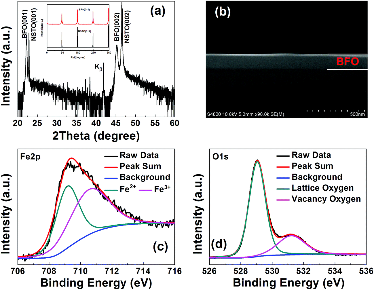 | ||
| Fig. 1 (a) XRD θ–2θ scan of the BFO/NSTO heterostructure, the inset is the ϕ-scans of the BFO (011) and NSTO (011) planes, respectively. (b) The cross-sectional SEM image of the heterostructure. Core-level XPS spectrum of Fe2p3/2 (c) and O1s (d) of the BFO film. Each spectrum is fitted with the Gaussian curve fitting method. | ||
Fig. 2(a) shows typical current–voltage (I–V) characteristics of the Pt/BFO/NSTO heterostructure on a semi-log scale, the inset shows a schematic illustration of the device. A positive direction of the current was defined as from the top electrode towards the bottom electrode. The voltages were applied by the sequence of 0 V → +3 V → 0 V → −5 V → 0 V, where the arrows indicate the sweeping direction. The device exhibits typical bipolar RS behavior without a forming process, which is opposite to the results of Chen et al. when using Au/BiFeMnO3/Pt structure, indicating a different RS mechanism from the conductive filament proposed by Chen.13 As shown in Fig. 2(b), the resistances at HRS-1, HRS-2 and LRS remain unchanged after continuously reading at −0.1 V for 103 s, revealing good retention characteristics, which is comparable with that obtained in the Pt/BFO/NSTO heterostructures reported by Hu et al.12 and Wang et al.14 Furthermore, our Pt/BFO/NSTO heterostructure shows multilevel RS behavior by applied different reset voltages (Vreset). As illustrated in Fig. 2(c), the applied sweeping voltage was applied as +3 V → 0 V → Vreset → 0 V → +3 V. When the Vreset is −1 V, no obvious RS window in the I–V curve is observed. However, with the increase in the Vreset, the RS window increases and the device exhibit multilevel RS effect. It is also found that in the negative region of the I–V loop, an obvious negative differential resistance phenomenon is demonstrated when the Vreset exceeds −2 V. The differential resistance phenomenon has also been reported in other articles, which can be explained by the variance of space charge region and trapping/detrapping of electrons by interface state.6,8,27
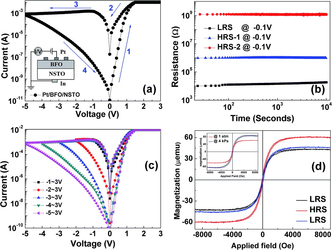 | ||
| Fig. 2 (a) Typical I–V characteristics of the Pt/BFO/NSTO heterostructure in a semi-log scale, the inset shows a schematic illustration of the device. (b) Retention characteristics of the device at HRS-1, HRS-2 and LRS. (c) Multilevel RS behavior of the device. (d) Magnetic loops of the device at HRS and LRS. The inset is magnetic loops of BFO film that cooling in different oxygen pressure of 1 atm and 4 kPa. | ||
As mentioned above, BFO is a typical antiferromagnetic material in bulk form and weak ferromagnetic material in the film form.28 Therefore, it is essential to investigate the effects of RS on the magnetic properties of the BFO film. To obtain strong magnetic signals induced by the RS effect, a Pt/BFO/NSTO heterostructure with 14 resistance cells are switched consistently for the magnetization measurements. A maximum magnetic field of 1 T in the direction perpendicular to the film surface is applied during the measurements. The diamagnetic signals of the substrate are deducted from the raw hysteresis loops and all the measurements were carried out at room temperature. Fig. 2(d) shows the magnetization loops of the BFO film at HRS and LRS. We can see that the saturation magnetization (Ms) of the BFO film shows reversible switching upon different resistance states, giving low Ms of 45 μemu at LRS while high Ms of 60 μemu at HRS. The rate of change in the Ms value at LRS and HRS can reach up to 33%, which is essential for practical applications. The coexistence of resistive and magnetization switching in the BFO film provides a possible way to design switchable multilevel memory and multi-field signal detection devices via both electricity and magnetism.
Previous studies have shown that the variation of magnetism in the oxide heterostructure is closely relevant to the content of oxygen vacancies in the oxide film.6,8,11 In order to investigate the role of the oxygen vacancies in regulation of the magnetism of the Pt/BFO/NSTO structure, we prepared another BFO sample under the same deposition conditions which was cooled in lower oxygen pressure of 4 kPa. As shown in the inset of Fig. 2(d), the magnetization of the sample in a higher cooling oxygen pressure of 1 atm is obviously smaller than that in a lower cooling oxygen pressure of 4 kPa. As the previous study has shown that the cooling process in a lower oxygen pressure can introduce more oxygen vacancies in the interior of the BFO films than that in a higher oxygen pressure.29 This might imply that the concentration of oxygen vacancies in the BFO films show a close relationship with the corresponding magnetism.
In order to further investigate the physical mechanism related to resistive and magnetization switching of the Pt/BFO/NSTO heterostructure, analysis on the internal conductive transport properties is necessary. The most possible conductive mechanisms include space-charge-limited conduction (SCLC), Schottky emission (SE) and Poole–Frenkel emission (PF).30–32 Fig. 3(a) plots the I–V curves of the Pt/BFO/NSTO heterostructure at positive bias region. It shows that the I–V transport characteristics belongs to the SCLC, which is consistent with other research reports.27 This suggests that the defects in the films such as oxygen vacancies play an important role in the transport process. Fig. 3(b) shows the ln(−I) vs. ln(−V) plot based on the data from Fig. 2(a) (0 V to −1 V) in the negative bias region of the LRS. The curve shows linear behavior with a slope of 2, corresponding to the SCLC mechanism. Fig. 3(c) and (d) show the ln(I/V) versus V1/2 plots based on the data from Fig. 2(a) (−1 to −5 V and −5 V to 0 V, respectively). The curves show linear behavior, corresponding to the PF emission mechanism. Therefore, the conduction behavior of the set process and the LRS can be explained using SCLC mechanism, and the HRS in the negative voltage region can be explained by PF emission. This behavior is also consistent with that reported previously on interfacial effects, where oxygen vacancy migration and charge trapping/detrapping at the interface drive RS in various heterostructures.6,8,11,30
 | ||
| Fig. 3 Plots of the I–V curves in Fig. 2(a) on different scales to reveal their conduction mechanisms: (a) positive bias region plotted in log–log scale; (b) ln(−I) vs. ln(−V) in the negative bias region (0 to −1 V) at LRS. (c) ln(I/V) vs. (−V)1/2 in the negative bias region (−1 to −5 V). (d) ln(I/V) vs. (−V)1/2 in the negative bias region (−5 to 0 V). | ||
Based on the experimental results and analysis above, the correlation changes of the resistance and magnetism of the devices can be attributed to the modulation effect of the ferroelectric polarization reversal on the width of depletion region and the height of potential barrier via the charge trapping and detrapping process combined with the migration of oxygen vacancies at the BFO/NSTO interface. The Fig. 4 shows the schematic diagrams of the energy band of RS and magnetization switching of the Pt/BFO/NSTO device. As shown in Fig. 4(a), when the positive voltage is applied to the device, the ferroelectric polarization in the BFO film points downward. Because of the ferroelectric field effect, the oxygen vacancies migrate towards the interface of the BFO/NSTO and the electrons in NSTO would inject into the depletion layer at the interface, resulting in the decreases in the depletion width and the barrier height. Subsequently, the electrons would pass over the barrier and inject into the BFO films, and eventually, be trapped by the oxygen vacancies, which correspond to the RS behavior from HRS to LRS. As can be seen in Fig. 4(b), when the reverse voltage was applied to the device, the ferroelectric polarization in the BFO films points upward, resulting in the increase in the depletion width and the height of the barrier. At the same time, the electrons might be detrapped and migrate towards the bottom electrode while the oxygen vacancies migrate backwards into the BFO films, which correspond to the RS from LRS to HRS.
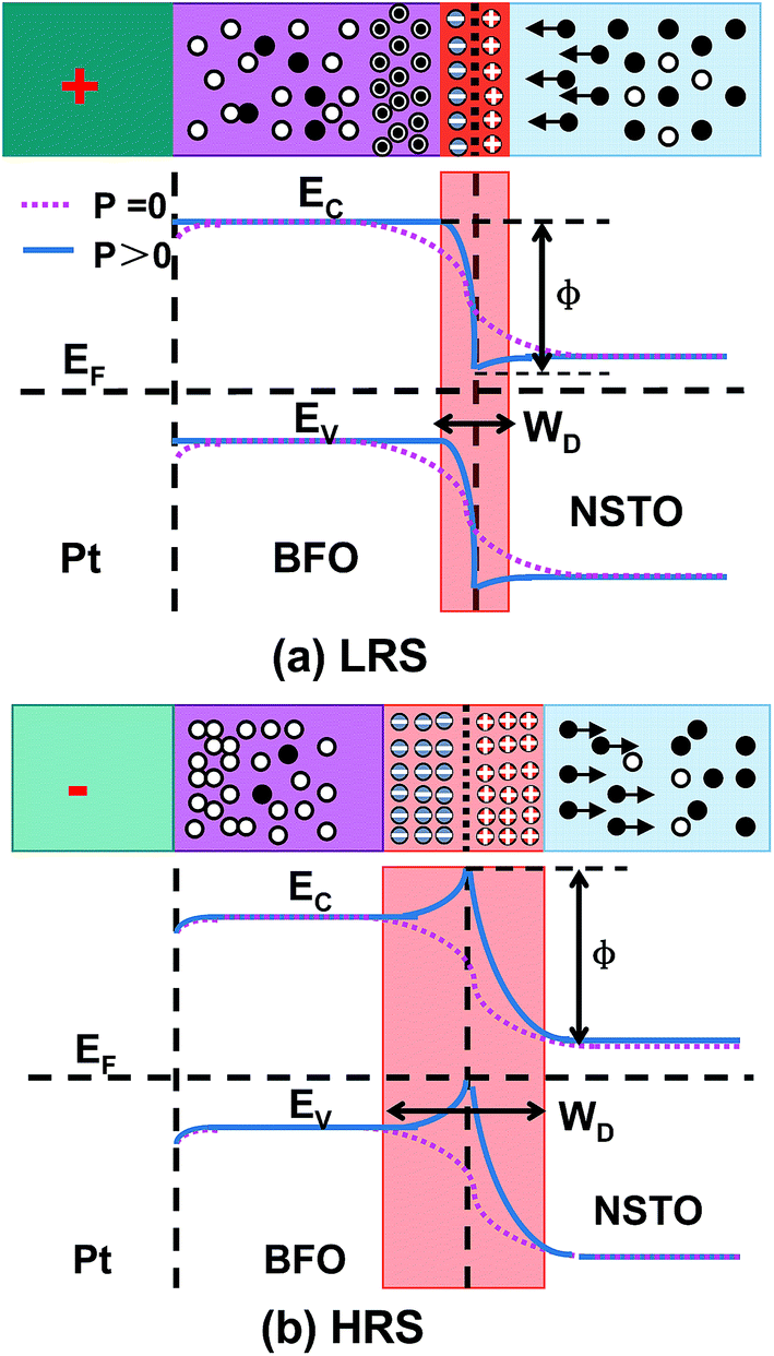 | ||
| Fig. 4 Schematic charge distribution and energy diagrams of the Pt/BFO/NSTO heterostructure at LRS and HRS. The “plus” and “minus” symbols represent ionized acceptors and donors; the white circle and black dot symbols represent holes and electrons, respectively; the circle with the black dot in its center symbols represent electrons trapped by the oxygen vacancies. | ||
Typical BFO crystal exhibits a rhombohedral phase (R3c) and a G-type antiferromagnetic structure with spiral spin modulation cycle of 62 nm, which usually can not show strong ferromagnetism.28 However, in the previous studies, the observed ferromagnetic behaviors of BFO thin films was attributed to the effect of the mismatch strain or the change of Fe ion valence state.33–36 Based on the first-principle calculations, Chen et al. found that Mn doping in the BFO films could lead to easy conversion of Fe ion between Fe3+ and Fe2+ because of the impurity energy level.13 Thus, the initial states of these films exhibit ferromagnetism. As for our BFO films, we speculate that the origin of ferromagnetism may be due to the change of valence state of iron ions because of inevitable oxygen vacancies introduced in the deposition process. Under the positive voltage, the device is set from HRS to LRS. Due to the ferroelectric field effect, the oxygen vacancies migrate towards the bottom electrode and gathering at the interface, while the injected electrons would neutralize the positive charge of the oxygen vacancies, and thus the number of oxygen vacancies in the internal of BFO films would decrease. The reduction of oxygen vacancies results in oxidation of partial Fe2+ to Fe3+, which would weaken the double exchange interaction between Fe2+ and Fe3+. Accordingly, the Ms in the LRS decreases. However, when the device is reset from LRS to HRS under the negative voltage, the oxygen vacancies at the interface detrap electrons and migrate backwards into the BFO films, which increases the concentration of oxygen vacancies in BFO films. Thus, partial Fe3+ are reduced to Fe2+, which could enhance the double exchange interaction between Fe2+ and Fe3+. Then the Ms in the HRS increases. Therefore, we achieve the regulation of both RS and Ms by the electric field, which exhibits nonvolatile, reversible and repeatable characteristics.
4. Conclusions
In conclusion, our Pt/BFO/NSTO device shows stable bipolar resistive switching characteristics with maximum Roff/Ron ratio of 105, good retention and multilevel memory properties. Moreover, the saturation magnetization of BFO film shows reversible switching associated with its resistance states. These resistive and magnetization switching characteristics can be attributed to the modulation effect of the ferroelectric polarization reversal on the width of depletion region and the height of potential barrier via the charge trapping and detrapping process combined with the migration of oxygen vacancies at the BFO/NSTO interface. The results of this study extend the application field of BFO in multiferroic RS multifunctional devices.Acknowledgements
This work was supported by the National Natural Science Foundation of China (Grant No. 11504101, 51372174, and 11364018), the Natural Science Foundation of Hubei Province (Grant No. 2014CFB610) and the Excellent Young Innovation Team Project of Hubei Province (Grant No. T201429).References
- G. I. Meijer, Science, 2008, 319, 1625 CrossRef CAS PubMed.
- D. B. Strukov, G. S. Snider, D. R. Stewart and R. S. Williams, Nature, 2008, 453, 80 CrossRef CAS PubMed.
- A. Sawa, Mater. Today, 2008, 11, 28 CrossRef CAS.
- T. L. Qu, Y. G. Zhao, D. Xie, J. P. Shi, Q. P. Chen and T. L. Ren, Appl. Phys. Lett., 2011, 98, 173507 CrossRef.
- L. Wang, K. Jin, C. Ge, C. Wang, H. Guo, H. Lu and G. Yang, Appl. Phys. Lett., 2013, 102, 252907 CrossRef.
- S. Ren, H. Qin, J. Bu, G. Zhu, J. Xie and J. Hu, Appl. Phys. Lett., 2015, 107, 062404 CrossRef.
- S. Ren, L. Zhang, J. Dong, Y. Huang, J. Guo, L. Zhang, J. Zhao, X. Zhao and W. Chen, J. Mater. Chem. C, 2015, 3, 4077 RSC.
- M. Zhao, Y. Zhu, Q. Wang, M. Wei, X. Liu, F. Zhang, C. Hu, T. Zhang, D. Qiu, M. Li and R. Xiong, Appl. Phys. Lett., 2016, 109, 013504 CrossRef.
- Y. Q. Xiong, W. P. Zhou, Q. Li, M. C. He, J. Du, Q. Q. Cao, D. H. Wang and Y. W. Du, Appl. Phys. Lett., 2014, 105, 032410 CrossRef.
- Y. Luo, D. Zhao, Y. Zhao, F. Chiang, P. Chen, M. Guo, N. Luo, X. Jiang, P. Miao, Y. Sun, A. Chen, Z. Lin, J. Li, W. Duan, J. Cai and Y. Wang, Nanoscale, 2015, 7, 642 RSC.
- Q. Wang, Y. Zhu, X. Liu, M. Zhao, M. Wei, F. Zhang, Y. Zhang, B. Sun and M. Li, Appl. Phys. Lett., 2015, 107, 063502 CrossRef.
- Z. Q. Hu, Q. Li, M. Y. Li, Q. W. Wang, Y. D. Zhu, X. L. Liu, X. Z. Zhao, Y. Liu and S. X. Dong, Appl. Phys. Lett., 2013, 102, 102901 CrossRef.
- G. Chen, G. Bi, L. Song, Y. Weng, D. Pan, Y. Li, S. Dong, T. Tang, J. M. Liu and J. G. Wan, Appl. Phys. Lett., 2016, 109, 112903 CrossRef.
- C. Wang, K. Jin, Z. Xu, L. Wang, C. Ge, H. Lu, H. Guo, M. He and G. Yang, Appl. Phys. Lett., 2011, 98, 192901 CrossRef.
- Y. Huang, Y. Wu, X. Wang, S. Zhang, X. Shia and H. Zeng, RSC Adv., 2016, 6, 17867 RSC.
- T. Zhao, A. Scholl, F. Zavaliche, K. Lee, M. Barry, A. Doran, M. Cruz, Y. Chu, C. Ederer and N. Spaldin, Nat. Mater., 2006, 5, 823 CrossRef CAS PubMed.
- R. Ramesh and N. A. Spaldin, Nat. Mater., 2007, 6, 21 CrossRef CAS PubMed.
- Y. H. Chu, L. W. Martin, M. B. Holcomb, M. Gajek, S. J. Han, Q. He, N. Balke, C. H. Yang, D. Lee and W. Hu, Nat. Mater., 2008, 7, 478 CrossRef CAS PubMed.
- Z. Hu, M. Li, Y. Zhu, S. Pu, X. Liu, B. Sebo, X. Zhao and S. Dong, Appl. Phys. Lett., 2012, 100, 252908 CrossRef.
- B. F. Yu, M. Y. Li, J. Wang, Z. Q. Hu, X. L. Liu, Y. D. Zhu and X. Z. Zhao, Thin Solid Films, 2012, 520, 4089 CrossRef CAS.
- B. Yu, M. Li, Z. Hu, L. Pei, D. Guo, X. Zhao and S. Dong, Appl. Phys. Lett., 2008, 93, 182909 CrossRef.
- J. Luo, S. Lin, Y. Zheng and B. Wang, Appl. Phys. Lett., 2012, 101, 062902 CrossRef.
- J. H. Jeon, H. Y. Joo, Y. M. Kim, D. H. Lee, J. S. Kim, Y. S. Kim, T. Choi and B. H. Park, Sci. Rep., 2016, 6, 23299 CrossRef CAS PubMed.
- B. Sun, Y. Liu, W. Zhao and P. Chen, RSC Adv., 2015, 5, 13513 RSC.
- D. Li, W. Zheng, D. Zheng, J. Gong, L. Wang, C. Jin, P. Li and H. Bai, ACS Appl. Mater. Interfaces, 2016, 8, 3977 CAS.
- L. Zhao, Z. Lu, F. Zhang, G. Tian, X. Song, Z. Li, K. Huang, Z. Zhang, M. Qin, S. Wu, X. Lu, M. Zeng, X. Gao, J. Dai and J. M. Liu, Sci. Rep., 2015, 5, 09680 CrossRef CAS PubMed.
- P. Wang, P. Li, Y. Zhi, D. Guo, A. Pan, J. Zhan, H. Liu, J. Shen and W. Tang, Appl. Phys. Lett., 2015, 107, 262110 CrossRef.
- Y. H. Chu, L. W. Martin, M. B. Holcomb and R. Ramesh, Mater. Today, 2007, 10, 16 CrossRef CAS.
- G. L. Yuan, L. W. Martin, R. Ramesh and A. Uedono, Appl. Phys. Lett., 2009, 95, 012904 CrossRef.
- H. Peng, G. Li, J. Ye, Z. Wei, Z. Zhang, D. Wang, G. Xing and T. Wu, Appl. Phys. Lett., 2010, 96, 192113 CrossRef.
- T. Fujii, M. Kawasaki, A. Sawa, Y. Kawazoe, H. Akoh and Y. Tokura, Phys. Rev. B: Condens. Matter Mater. Phys., 2007, 75, 165101 CrossRef.
- A. Odagawa, H. Sato, I. H. Inoue, H. Akoh, M. Kawasaki, Y. Tokura, T. Kanno and H. Adachi, Phys. Rev. B: Condens. Matter Mater. Phys., 2004, 70, 224403 CrossRef.
- J. Wang, J. B. Neaton, H. Zheng, V. Nagarajan, S. B. Ogale, B. Liu, D. Viehland, V. Vaithyanathan, D. G. Schlom, U. V. Waghmare, N. A. Spaldin, K. M. Rabe, M. Wuttig and R. Ramesh, Science, 2003, 299, 1719 CrossRef CAS PubMed.
- W. Eerenstein, F. D. Morrison, J. Dho, M. G. Blamire, J. F. Scott and N. D. Mathur, Science, 2005, 307, 1203 CrossRef CAS PubMed.
- C. Ederer and N. A. Spaldin, Phys. Rev. B: Condens. Matter Mater. Phys., 2005, 71, 224103 CrossRef.
- S. K. Kim, H. M. Jang and J. Chang, Journal of Magnetics, 2006, 11, 108 CrossRef.
Footnote |
| † These authors contribute equally to this work. |
| This journal is © The Royal Society of Chemistry 2017 |