
 Open Access Article
 This Open Access Article is licensed under a Creative Commons Attribution-Non Commercial 3.0 Unported Licence
Stretchable, alternating-current-driven white electroluminescent device based on bilayer-structured quantum-dot-embedded polydimethylsiloxane elastomer†
Soon Moon Jeong‡
 *a,
Seongkyu Song‡a,
Hyunmin Kima,
Seong-Ho Baeka and
Joon Seop Kwakb
*a,
Seongkyu Song‡a,
Hyunmin Kima,
Seong-Ho Baeka and
Joon Seop Kwakb
aDivision of Nano and Energy Convergence Research, DGIST, Daegu 711-873, Republic of Korea. E-mail: smjeong@dgist.ac.kr
bDepartment of Printed Electronics Engineering, Sunchon National University, Sunchon, Jeonnam 540-742, Republic of Korea
First published on 27th January 2017
Abstract
In this work, we demonstrate neutral/pure/cool white light due to color conversion from quantum dot (QD)-embedded, polydimethylsiloxane (PDMS)-based alternating-current-driven electroluminescent (ACEL) devices. White light generation is achieved by the spontaneously formed bilayer-structure emitting layer (b-EML) comprising QDs embedded in PDMS containing Cu-doped zinc sulfide (ZnS:Cu) particles (EL emitting layer), without ZnS:Cu (color conversion layer). Red light is generated by CdSe/CdZnS QDs, which partially absorbs electrically excited blue-green EL. This study examines the use of spontaneously formed b-EML as a means of alleviating the problems resulting from QD aggregation in PDMS and its effects on electro-optical performance of ACEL devices under stretching conditions.
Introduction
Mechanical stretchability is an essential requirement of various optoelectronic devices for overcoming the limitation of rigidity and brittleness in conventional devices. One strategy to achieve such stretchability in inorganic electronics is the use of semiconductor nanomaterials configured into “wavy” shapes. Intense research has been performed to develop stretchable structures by either employing intrinsically stretchable materials or different device configurations (e.g., buckled and wavy structures).1 The mechanical conformability in these devices could enable a wide range of potential applications requiring novel functions such as flexing, twisting, stretching, and folding.1,2To develop fully stretchable device structures, a polydimethylsiloxane (PDMS)-supported zinc sulfide (ZnS) composite structure, composed of both ZnS and PDMS (ZnS + PDMS), has recently received considerable attention because of the resultant intrinsic stretchability and electroluminescence3–5 as well as mechanically excited luminescence (i.e., mechanoluminescence).5–12 With the use of transparent stretchable electrodes (e.g., silver nanowires), this PDMS-based structure in the form of a powder-based ZnS + PDMS film exhibits alternating-current electroluminescence (ACEL) characteristics with good performance in large strain cycles. In this case, the PDMS acts as both a dielectric material and a binder. Although the low dielectric constant of PDMS reduces its suitability for use in bright EL devices, more recently, this problem has been overcome by adding barium titanate (BaTiO3) particles to the composite, which leads to a focused electric field to the electroluminescent (EL) particles for improved light emission.4 For better stretchability, the application of an ionic conductor as binders or electrodes has also been reported.13,14 However, different color control technologies or white ACEL devices with this structure have not yet been demonstrated. The simplest approach for different color control involves control of the concentration of different-color-emitting phosphors.7,9,15,16 For example, white EL can be realized by mixing blue and orange phosphors. However, sulfide-based red-emitting phosphors are chemically unstable and show luminescence saturation with an increasing applied current when incorporated into white LEDs.17,18 Another simple approach involves the use of a down conversion method based on long-wavelength light emission by absorbing short-wavelength light.15,16 There are several types of wavelength-converter materials including semiconductors and organic dyes. Organic dyes possess good photoluminescent properties, but organic molecules lack long-term stability owing to their photooxidative and thermally unstable characteristics.16,18,19 In contrast, nanocrystal quantum dots (QDs) have been considered as the most promising down conversion materials in light-emitting applications because of their high PL quantum yield, broad absorption spectrum, size-tunable emission, high resistance to photo-oxidation, and good color saturation. Several studies have attempted to realize white light from inorganic LEDs by using QDs as a down converter material.18,20–25
In this study, we demonstrate a stretchable, AC-driven white EL device based on spontaneously formed bilayer-structured emitting layer (b-EML) comprising QDs embedded with PDMS containing ZnS (bottom layer, ZnS + PDMS:QDs) and without ZnS (upper layer, PDMS:QDs). In general, lumpy aggregates of QDs induce lower extraction of EL owing to reabsorption.26 It is therefore desirable to employ color conversion materials in the form of thin layers, if QD aggregation is inevitable.16 In this regard, the proposed bilayer structure exhibits two novel functions: it enables efficient light conversion without leakage of EL by covering the phosphor particles completely and acts as a thin color conversion layer reducing light loss from the usually formed QDs aggregates in the polymer matrix.23–28 We also demonstrated that white ACEL devices emit natural/pure/cool white light using this approach, which is expected to be a viable and common method for broader color expression in future ACEL applications.
Experimental
ACEL device fabrication
The ACEL device comprised three layers, PDMS(AgNW + PDMS)/b-EML/(AgNW + PDMS)PDMS, which is an EL emissive stretchable structure. The detailed fabrication is illustrated in Scheme 1 and Fig. S1 (ESI†). First two AgNW-embedded PDMS plates (approximately 300 μm-thick) using a transferring process from poly(methyl methacrylate) (PMMA) (approximately 200 nm) coated glass to PDMS. Initially, AgNWs dispersed in ethanol (AgNWs-40, ACS Material) were spin-coated onto a PMMA-coated glass substrate (300 and 100 rpm for the top and bottom plates, respectively) and subsequently dried at 100 °C for 1 min. Then, a part of the AgNWs was removed with tape to form an electrode with an active emitting area of 1 × 2 cm2 at the intersection of the bottom and top AgNW strips. Liquid PDMS (ELASTOSIL RT601, Wacker) with a curing agent at a weight ratio of 9![[thin space (1/6-em)]](https://www.rsc.org/images/entities/char_2009.gif) :1 was casted on top of the AgNW film with subsequent curing at 70 °C for 35 min under Al mold pressure for uniform thickness. After being peeled off the glass, the AgNWs were embedded at the surface of the cured PDMS, forming a conductive and stretchable layer. For the bilayer-structured emitting layer, first QDs dispersed in toluene (20 mg ml−1, ECOFLUX) and liquid PDMS were mixed at a weight ratio of 1:0.9 and dried in a vacuum oven overnight in order to evaporate the solvent (0.9 is a considered value for the addition of curing agent (0.1) in the next procedure). After evaporating the toluene, the QDs + PDMS and liquid PDMS were mixed at a weight ratio of 1:0.9 once more, and blue-green phosphor (GG24, Global Tungsten & Powders Corp.) was uniformly mixed, and then, curing agent (0.2) was added for a total weight ratio of 7:3 (QDs + PDMS:phosphor). Note that the weight ratio of the liquid PDMS and the curing agent is maintained at 9:1. Here, the final weight ratio of QDs + PDMS:curing-agent:phosphor is 1.8:0.2:(6/7) for QD-ACEL(B) and QD-ACEL(C) devices. Basically, we used the same QDs + PDMS as the base material and controlled the PDMS weight in the 2nd mixing procedure to prepare QDs embedded PDMS with different concentrations. Thus, for QD-ACEL(A), the PDMS with a weight ratio of 2.7 is added to QDs + PDMS during the 2nd mixing procedure. This QDs + PDMS + phosphor mixture is subsequently sandwiched between previously prepared AgNW-embedded PDMS layers and is cured overnight in an oven at 70 °C.
:1 was casted on top of the AgNW film with subsequent curing at 70 °C for 35 min under Al mold pressure for uniform thickness. After being peeled off the glass, the AgNWs were embedded at the surface of the cured PDMS, forming a conductive and stretchable layer. For the bilayer-structured emitting layer, first QDs dispersed in toluene (20 mg ml−1, ECOFLUX) and liquid PDMS were mixed at a weight ratio of 1:0.9 and dried in a vacuum oven overnight in order to evaporate the solvent (0.9 is a considered value for the addition of curing agent (0.1) in the next procedure). After evaporating the toluene, the QDs + PDMS and liquid PDMS were mixed at a weight ratio of 1:0.9 once more, and blue-green phosphor (GG24, Global Tungsten & Powders Corp.) was uniformly mixed, and then, curing agent (0.2) was added for a total weight ratio of 7:3 (QDs + PDMS:phosphor). Note that the weight ratio of the liquid PDMS and the curing agent is maintained at 9:1. Here, the final weight ratio of QDs + PDMS:curing-agent:phosphor is 1.8:0.2:(6/7) for QD-ACEL(B) and QD-ACEL(C) devices. Basically, we used the same QDs + PDMS as the base material and controlled the PDMS weight in the 2nd mixing procedure to prepare QDs embedded PDMS with different concentrations. Thus, for QD-ACEL(A), the PDMS with a weight ratio of 2.7 is added to QDs + PDMS during the 2nd mixing procedure. This QDs + PDMS + phosphor mixture is subsequently sandwiched between previously prepared AgNW-embedded PDMS layers and is cured overnight in an oven at 70 °C.
 | ||
| Scheme 1 Schematic of the ACEL device fabrication process. (a) Spin-coating of the AgNW solution (dispersed in ethanol) onto the PMMA (200 nm) coated glass at 100 and 300 rpm for the bottom and top electrodes, respectively. After evaporating the ethanol at 100 °C for 1 min, (b) a part of the AgNWs was removed with tape to form patterned electrodes. Then, the PDMS solution was dropped onto the AgNW-coated glass, and (c) two flat PDMS base plates (top and bottom) with uniform thickness were fabricated after curing at 70 °C for 35 min using an Al mold. After the delamination of the PDMS, (d) the QDs + ZnS + PDMS mixture was dropped and a flat EML layer was constructed using the Al mold (70 °C overnight). (e) The film was cut to the desired sample dimensions. | ||
Electro-optical characterization
The EL spectra were measured under a sinusoidal voltage of 400 V with various frequencies (50, 100, 300, 500, 800, 1000, 1500, and 2000 Hz) from a function generator (AFG3102, Tektronix) with a voltage amplifier (623B, Trek). During stretching, the current was measured using a current meter (3706A, Keithley), and the light emission was observed using the combination of a spectrometer (QEPro, Ocean Optics, Inc.) and a vertically aligned optical fiber equipped with a collimating lens. To measure the brightness, a spectroradiometer (PR-670, Photo Research Inc.) was used. The CIE coordinates were calculated from the measured EL spectra, and the correlated color temperatures (CCTs) were calculated using McCamy approximation. The optical absorption, transmittance, and photoluminescence (PL) were measured using a UV-Vis-NIR light source (DH-2000-BAL, Ocean Optics), diode laser (TEM-F-405, EFORCE), and spectrometer (USB4000-XR1-ES, Ocean Optics).Two-photon excitation fluorescence (TPEF) microscopy
A 100 fs, 80 MHz commercial Ti:sapphire oscillator (Insight Deepsee Dual, Spectra-Physics) was employed as a pump source. For 3D image scanning, the beam was guided to a commercial galvanoscanner (Fluoview 1000, Olympus) assembled to inverted confocal microscopes (IX83, Olympus), where a photomultiplier tube (R3896 PMT, Hamamatsu) was used to detect the epi-scattered TPEF photons. A wavelength of 800 nm (∼1 mW at the sample) was chosen to obtain comparable TPEF intensities at 520 nm (FF01-520/15, Semrock) with a bandwidth of 15 nm associated with the two-photon absorption (400 nm) of the QDs. The zoomed-in TPEF views in PDMS:QDs were extracted from the 3D image stacks scanned in the z-direction with a 3 μm depth interval.Results and discussion
An optical microscope image shown in Fig. 1a represents the spontaneously formed b-EML, which consists of ZnS + PDMS:QDs or PDMS:QDs. The bilayer is formed by sinking ZnS in the liquid PDMS owing to the larger specific gravity of ZnS (4.10) than that of PDMS (1.03).29 This b-EML is sandwiched between silver nanowires (AgNWs) buried at the surface of the cured PDMS that allow electrical conduction and transmittance under the stretching condition (Fig. 1b). This optical image also shows well-laminated PDMS/(AgNW + PDMS)/b-EML/(AgNW + PDMS)/PDMS layers prepared by using the molding fabrication process. As an EL light source, we used ZnS doped with a Cu phosphor (ZnS:Cu) that generates blue-green light (Fig. 1c) and found that the ZnS particle is composed of two phases, namely cubic (F![[4 with combining macron]](https://www.rsc.org/images/entities/char_0034_0304.gif) 3m) and hexagonal (P63mc) structures (Fig. 1d). For color conversion, we used commercially available CdSe/CdZnS core/shell QDs with long chain amine ligand (diameters of ∼7 nm, ECOFLUX, Fig. 1e). Fig. 1f shows EL and PL spectra from ZnS and QDs, respectively, which shows blue-green and red colors, respectively. The broadband absorption of QDs is also introduced over the entire wavelength range, which can generate excitons from QDs. The simple principle for white EL is also denoted by an arrow in Fig. 1a: some of the blue-green EL is absorbed in the QDs and re-emitted as red light with a longer wavelength. As a result, white light composed of two main wavelengths could be achieved by combining the blue-green and red light.
3m) and hexagonal (P63mc) structures (Fig. 1d). For color conversion, we used commercially available CdSe/CdZnS core/shell QDs with long chain amine ligand (diameters of ∼7 nm, ECOFLUX, Fig. 1e). Fig. 1f shows EL and PL spectra from ZnS and QDs, respectively, which shows blue-green and red colors, respectively. The broadband absorption of QDs is also introduced over the entire wavelength range, which can generate excitons from QDs. The simple principle for white EL is also denoted by an arrow in Fig. 1a: some of the blue-green EL is absorbed in the QDs and re-emitted as red light with a longer wavelength. As a result, white light composed of two main wavelengths could be achieved by combining the blue-green and red light.
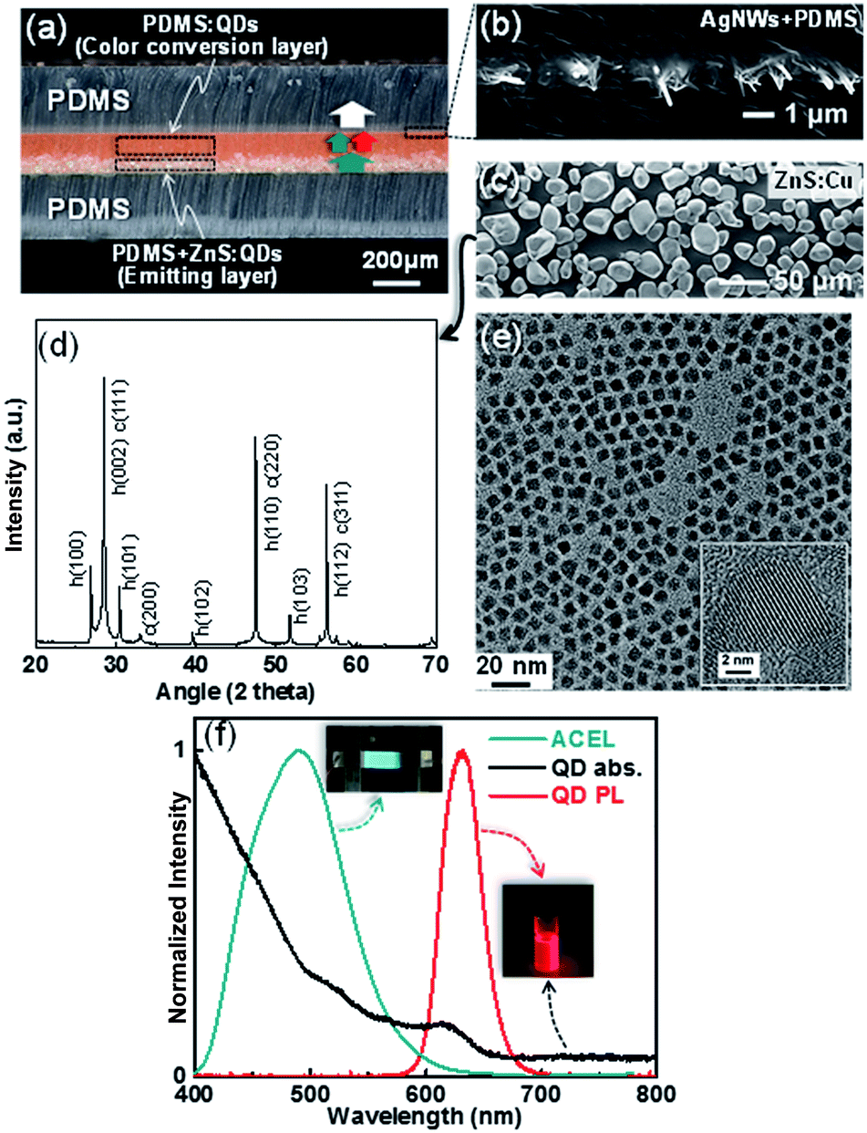 | ||
| Fig. 1 (a) Optical microscope image of the proposed ACEL device and experimental approach used in this study; some of the blue-green EL is absorbed in the PDMS:QDs and re-emitted as red light with a longer wavelength, forming white light composed of blue-green and red light. (b) Cross-sectional SEM image showing AgNW-embedded PDMS. (c) SEM image and (d) X-ray diffraction results of ZnS:Cu phosphors used in this work. (e) TEM image of QDs. (f) Absorption (black) and PL (red) spectra obtained from QDs dispersed in toluene. The EL spectrum obtained from the reference ZnS + PDMS sample is also shown by the blue-green line (insets: EL and PL images of EL device and colloidal QDs, respectively). | ||
It is important that the QDs have a well distributed PDMS film homogeneously inside because the status of the QDs considerably affects the light extraction and color conversion characteristics. We therefore prepared two simplified PDMS-supported PDMS:QD films with different mixing weight ratios of QDs (PDMS:QDs-A, PDMS:QDs-B) by removing ZnS phosphors and AgNWs, which can be regarded as additional factors (Table 1). We used a molding process to prepare a PDMS/PDMS:QDs/PDMS three-layered stacking structure. The center-positioned PDMS:QDs are prepared by directly dispersing the colloidal QDs (solvent: toluene) into the PDMS monomer because toluene is also a good solvent for the PDMS. Fig. 2a and b shows the cross-sectional optical images of the two prepared samples with an approximately 125 μm-thick PDMS:QD layer sandwiched by two PDMS layers with stretching characteristics (inset of Fig. 2c). With the naked eye, we could observe the background image by transparent PDMS:QDs samples (Fig. 2c). However, we found that the transmittance of each sample was just 35% and 48% (at 550 nm), respectively, which indicates scattering characteristics (Fig. 2d). Basically, if there are no scattering centers in the films, the transmittance over the 650 nm wavelength range should be at a similar level as that of bare PDMS because QD absorption starts from 650 nm and increases over a shorter wavelength region (green line, Fig. 2d). To observe the in situ QDs distribution films inside, we employed two-photon excitation fluorescence (TPEF) microscopy that offers inherent ∼300 (in-plane) × 1000 (depth) nm resolution. This technique is beneficial for in-plane observation of the light-emitting particles without slicing the samples. An 800 nm wavelength was chosen as the two-photon excitation source for red emissions from the QDs. Fig. 2e and f show the TPEF image of the QD in-plane distribution of the two samples. Micrometer-sized (approximately 4–5 μm) particles were mostly distributed in the films because of QD aggregation (Fig. 2g). In particular, in the case of highly concentrated QDs (PDMS:QDs-A), large aggregates (>5 μm) are sparsely observed (upper, Fig. 2g), which means that the concentration of QDs plays a major role in determining the aggregate size. As a result, the transmittance decreases with the introducing QDs because a few micrometer-sized lumpy aggregates induce scattering of the incident light. Furthermore, this possibly results in lower extraction efficiency in ACEL devices owing to reabsorption during scattering.
| Samples | Mixing weight ratio | Average thickness (μm) | ||
|---|---|---|---|---|
| QDs solution (2 wt%) | PDMS | PDMS:QDs | Total | |
| Reference (pure PDMS) | — | — | — | 195.9 |
| PDMS:QDs-A | 1 | 2 | 129.0 | 730.7 |
| PDMS:QDs-B | 1 | 4 | 125.3 | 717.7 |
 | ||
| Fig. 2 (a) and (b) Optical microscope images of PDMS:QDs sandwiched by PDMS. (c) Photograph of the three prepared samples (bare PDMS, PDMS:QDs-A, PDMS:QDs-B) containing different amount of QDs. (d) Transmittance of three samples. Absorption of QDs also shown as green line to verify the effects of QDs on transmittance. (e) and (f) TPEF images showing QD distribution inside the PDMS:QD layer. (g) Line profiles denoted as dotted line in (e) and (f). | ||
In principle, the transparency of the PDMS:QDs should be further improved to avoid problems of scattering and reabsorption when applied to devices. A few approaches have been proposed to disperse QDs in polymers uniformly through ligand exchange,30 the use of hydrophobic polymers,23 and additional silica encapsulation of QDs.24 However, there has been no systematic, fundamental work on avoiding QDs flocculation when they are embedded in a polymer matrix. Hence, it is promising to use aggregated QDs themselves without any complex pre- or post-treatment if the aggregated state does not seriously affect device performance. Thin film type scattering layers generally have larger light extraction than thick film ones because of reduced scattering and reflection. Hence, we adopted a spontaneously formed PDMS:QD layer as a thin color conversion layer positioned within the EML even though the existence of this layer increased the driving voltage owing to its own thickness. Apart from the scattering effect, we also note that the size of QD aggregates is smaller than that of the phosphor particles (average diameter of ∼25 μm). It should be noted that mixed colors are seen as a uniform color to the naked eye owing to the color-mixing concept; recognition of the small emission centres is not possible.7 Therefore, it can be mentioned that QD aggregation does not seriously affect the uniformity of the emitting area. In this sense, the use of QDs for color conversion in a stretchable ACEL device is a promising concept, particularly for white light.
Thus far, we described the QDs distribution within the PDMS. We now discuss effects of QDs for white light in ACEL device. To observe the effect of PDMS:QDs on performance for different colors, ACEL devices with different b-EML conditions were prepared (Table 2), which are hereafter referred to as QD-ACEL-A, QD-ACEL-B, and QD-ACEL-C. The average thickness b-EML for each device is 168.8 μm, 190.3 μm, and 187.8 μm, respectively; the thickness was controlled for comparison with the reference device (no QDs, 169.9 μm) (Table 2). Fig. 3a shows the CIE coordinates of EL with varying electrical frequencies under different b-EML conditions. As the electrical frequency increases, the CIE coordinates of each sample shifts lower in the color space owing to an increase in the blue component of EL spectra. Because the Cu-doped ZnS phosphor used in the present work is highly susceptible to electrical frequencies, the emission color changes from green to blue with the increase in the blue peak as the excitation forces increase owing to existence of two emission bands (blue and green) in the phosphor (Fig. 3b).5,7–11 In the present work, since QD acts as an emitter as well as a broadband absorber, the resultant emitting color is highly dependent on the electrical frequency affecting ZnS:Cu ACEL. For example, at a low electrical frequency (50 Hz), the blue-green peak normalized QD peak intensities of the QD-ACEL samples (QD-ACEL-A, B and C) are 1.25, 0.74, and 1.52, respectively (Fig. 3c, upper), whereas they increase with electrical frequency (2 kHz) to 2.09, 1.30 and 2.70, which is an increase of approximately 70% (Fig. 3c, bottom). Since the absorption of QDs increases in the shorter wavelength region, QD absorption becomes more effective at high electrical frequencies resulting in increase in the QD peak. Consequently, this wavelength dependent absorption induces a down shift of the CIE coordinates approaching various white colors, showing that the CIE coordinates of the samples are (0.3269, 0.3314), (0.2813, 0.3239), and (0.3671, 0.3479). These three white colors also have different correlated color temperatures (CCTs), which can be described as cool and neutral white (Fig. 3d). In particular, we note that QD-ACEL-A shows a white color that is very close to pure white (namely, equal energy point) at a 2 kHz electrical frequency condition. We also compared the voltage dependencies of the three QD-ACEL devices with that of the reference under the same electrical frequency (2 kHz, Fig. 3e). The brightness of the reference does not exhibit a large difference from those of other published papers on PDMS-supported ACEL devices. PDMS is not a good choice of binder material for high brightness EL because its low dielectric constant (2.8) only yields a brightness value of around 10 cd m−2. A high dielectric material such as BaTiO3 can improve the brightness to over 100 cd m−2.4 However, the employment of QDs decreases the brightness of ACEL (QD-ACEL-A) when compared with the reference with similar b-EML thickness. The other QD-ACEL devices (QD-ACEL-B and QD-ACEL-C) show similar brightness values, but these values are lower than those of the reference and QD-ACEL-A, because of the weaker electric field resulting from the thicker b-EML. Consequently, brightness was lost to some extent by introducing QDs although this yielded various white colors. In the present work, however, we noted that the decrease in brightness can be improved if we successfully disperse QDs into PDMS. If we employ the uniformly distributed PDMS:QD composites, we can improve the brightness of the QD-ACEL devices by minimizing the reabsorption and scattering effects, which would lead to a decrease in brightness. We also found that the difference in peak wavelengths between QDs dispersed in toluene (630 nm, Fig. 1f) and PDMS (642 nm, Fig. 3c). The difference could be a result of the aggregation of QDs in PDMS and the effect of the changed surface and surrounding medium, which affected the excitonic binding energy of the QDs to some extent.17,28 We also comment on the high driving voltage owing to the positioning of the color conversion layer within the EML. In general, the brightness of ACEL devices is mainly determined by the EML thickness.15 It is always desirable to have high brightness for EL even under low AC voltage. However, brightness and color conversion efficiency are inversely related. Decreasing the EML thickness increases the EL brightness by increasing the electric field, but simultaneously decreases the color conversion of EL by decreasing the number of QDs, whereas increasing the EML thickness creates the opposite situation. Moreover, the transmittance of the AgNW-embedded PDMS film was only ∼47% (at 550 nm) even in the thin AgNW electrode, which is one major obstacle to improving the brightness (Fig. S2, ESI†). Hence, to resolve the large driving voltage, QD aggregation should be improved to increase the effective color conversion area even in thinner PDMS:QD layers. Also, from the view point of AgNW electrodes, the transmittance should be improved to minimize the negative effect on EL brightness. Ionic conductors with high transmittance13 can be used as alternative electrodes for improved brightness. A study on the dispersion of QDs and the application of ionic conductors is currently in progress.
| Samples | Mixing weight ratio | Average thickness (μm) | |||
|---|---|---|---|---|---|
| QDs solution (2 wt%) | PDMS | b-EML (ave.) | AgNW/PDMS (upper) | Total | |
| Reference | — | — | 169.9 | 303.7 | 746.9 |
| QD-ACEL-A | 1 | 2 | 190.3 | 277.3 | 744.6 |
| QD-ACEL-B | 1 | 4 | 168.8 | 277.7 | 723.3 |
| QD-ACEL-C | 1 | 2 | 187.8 | 285.7 | 747.4 |
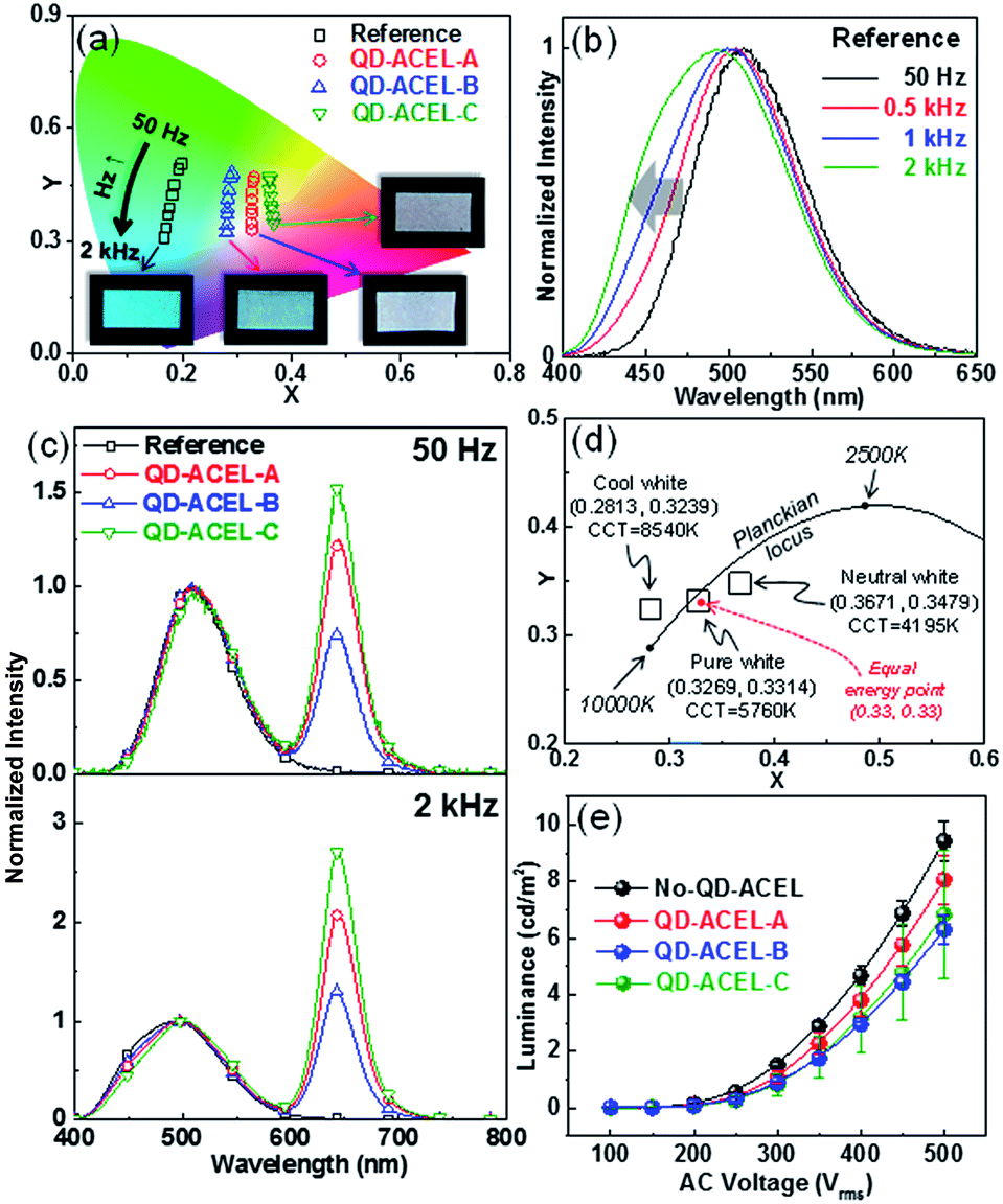 | ||
| Fig. 3 (a) CIE coordinates (x, y) calculated from the EL spectra (400 V) of four ACEL devices with different amounts of QDs and b-EML thicknesses under various electrical frequencies (insets: EL images at 2 kHz). (b) EL spectra obtained from the reference sample under different electrical frequencies. As the frequency increases, the blue component of spectrum also increases. (c) Blue-green peak normalized EL spectra obtained from EL devices driven by 50 Hz (upper) and 2 kHz (bottom) under same 400 V conditions. (d) Magnified CIE coordinates of various white EL under 2 kHz frequency condition. (e) Voltage–luminance data (at 2 kHz). | ||
Based on various white colors emitted from ACEL devices, we now describe the changes in the performance when the devices are stretched. Because current ACEL devices mainly consist of stretchable PDMS and AgNW electrodes, white EL is sustained without short circuit even when the device is manually stretched (Fig. 4a). To verify the effects of stretching, we observed the major factors such as luminous intensity, electrical current, and CIE coordinates. Maximum luminous intensity variation is observed when the device is stretched under the constant applied voltage. Because the sandwich structure of the device in the AC field can be treated as a capacitor, one can intuitively consider that the highest EL intensity should be observed at the maximum elongation condition owing to the minimized active layer (b-EML) thickness, which corresponds to an increased capacitance of the active layer. The increased capacitance enabled a larger AC current flow through the dielectric layer, resulting in an increased EL intensity. However, in our observations, the intensity of the spectra increases up to 40% elongation and decreases with further increase in the stretching distance (Fig. 4b and c). This result can be explained by the increase in the AgNW resistance as the stretching distance increases. In general, the emission intensity of the ACEL device, a type of field-driven device, is mainly determined by the bias voltage rather than by the conductive components of the current. Hence, even when the AgNW resistance was increased with increased stretching distance, the EL intensity and current were more sensitive to changes in the electric field. However, if the resistance increases, the actual voltage can be reduced through the generation of a voltage drop in the increased AC current condition at the 2 kHz frequency. Hence, the behaviours of the EL intensity and AC current over 40% elongation were decreased by the stretching distance, which corresponded to the simultaneously measured EL and AC current (Fig. 4c and d).
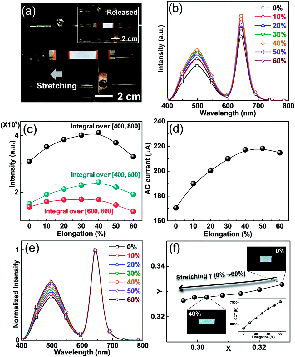 | ||
| Fig. 4 (a) Photograph of the white light emitting ACEL device (QD-ACEL-A) under released (inset) and stretched condition (40%). EL spectra (b), integrated values (c) and current behavior (d) under stretching conditions from 0 to 60%. (e) Red peak normalized spectra. Blue-green spectrum gradually increases as stretching distance increases. (f) Changes in CIE coordinates and CCT (inset) during stretching up to 60%. | ||
Besides this tendency, we also observe different behaviours in the two peaks originating from ZnS:Cu and QDs, namely the blue-green and red peaks. We integrated the area of each spectrum to visualize their tendencies (Fig. 4c). We found that the blue-green spectrum gradually increases up to 40% elongation whereas the red one does not show noticeable difference between the 20 and 40% elongation. To explain these behaviours, there are two issues to be discussed. In the initial stage, the blue-green spectrum increases as the stretching distance increase because an increase in the capacitance results in a larger AC current flow. In the case of the red one, however, a gradual increase is observed up to 30% elongation without noticeable changes. This phenomenon can be explained by reduction of thickness of the b-EML layer by the increase in the stretching distance. Because the spontaneously formed color conversion layer (PDMS:QDs), a part of b-EML, also decreases with elongation, the decrease in the ACEL passing distance results in a reduction of absorption, which would lead to a reduced red and increased blue spectrum.
We also noted the color changes of ACEL during the stretching. Based on the reduced thickness of the color conversion layer during stretching, the relative peak intensity of the blue-green peak linearly increases with the stretching distance (Fig. 4e) although the integration value of the EL intensity shows saturation behaviour (Fig. 4c). This preferential intensity change in the blue-green spectrum also affects the color conversion characteristics, as shown in Fig. 4f. Basically, the color is not affected by the absolute intensity of the spectrum. Therefore, the CIE coordinates shift to the bluish region owing to an increase in the blue-green intensity, as shown in normalized in red. The CCT values increase with the elongation distance because the increase in the blue color denotes a high color temperature (inset of Fig. 4f). Thus far, the color characteristics for stretchable light-emitting devices have not been considered as a major topic since most devices only include a single color emitting material. The stretching induced color changes, occurring from the multi-wavelength light, seem to be inevitable if we employ multi-layered structures such as the b-EML layer used in the present work. However, it is believed that such small color deviation is not serious under a dynamically deformed situation.
Conclusions
In this study, we demonstrated neutral/pure/cool white light from a stretchable ACEL device comprising mainly PDMS that can endure large strain. The white light could be obtained by the spontaneously formed bilayer structure containing QD-embedded PDMS acting as a color-conversion layer, which partially absorbs electrically excited blue-green EL. We observed micrometer-sized QD particles in the PDMS owing to their aggregation. However, we also found that this size of QD aggregates does not seriously affect white ACEL performance because human recognition of the small emission centres is not possible. We believe that our method, as demonstrated here, could be a viable and common method for manipulating broader color expression, and it will easily find applications in a broad range of applications involving stretchable devices.Acknowledgements
This work was supported by the Mid-career Researcher Program (NRF-2014R1A2A2A01003133) through the National Research Foundation of Korea (NRF) grant. This work was also supported by the DGIST R&D Program (16-NB-04) through DGIST, which is funded by the Ministry of Science, ICT and Future Planning (MSIP). J. S. K. acknowledges partial support from Basic Science Research Program through the NRF of Korea (NRF-2014R1A6A1030419).References
- J. A. Rogers, T. Someya and Y. Huang, Science, 2010, 327, 1603 CrossRef CAS PubMed; S. I. Park, Y. Xiong, R. H. Kim, P. Elvikis, M. Meitl, D. H. Kim, J. Wu, J. Yoon, C. J. Yu, Z. Liu, Y. Hung, K. C. Hwang, P. Ferreira, X. Li, K. Choquette and J. A. Rogers, Science, 2009, 325, 977 CrossRef PubMed; J. A. Rogers and H. H. Lee, in Unconventional Nanopatterning Techniques and Applications, ed. J. A. Rogers and H. H. Lee, John Wiley & Sons, Inc., New Jersey, United States of America, 2009, ch. 17 Search PubMed.
- T. Sekitani, H. Nakajima, H. Maeda, T. Fukushima, T. Aida, K. Hata and T. Someya, Nat. Mater., 2009, 8, 494 CrossRef CAS PubMed; J. Liang, L. Li, X. Niu, Z. Yu and Q. Pei, Nat. Photonics, 2013, 7, 817 CrossRef.
- J. Wang, C. Yan, K. J. Chee and P. S. Lee, Adv. Mater., 2015, 27, 2876 CrossRef CAS PubMed; J. Wang and P. S. Lee, Nanophotonics, 2016, 5, 81 Search PubMed.
- F. Stauffer and K. Tybrandt, Adv. Mater., 2016, 28, 7200 CrossRef CAS PubMed.
- S. M. Jeong, S. Song and H. Kim, Nano Energy, 2016, 21, 154 CrossRef CAS.
- D. Peng, B. Chen and F. Wang, ChemPlusChem, 2015, 80, 1209 CrossRef CAS.
- S. M. Jeong, S. Song, S. K. Lee and N. Y. Ha, Adv. Mater., 2013, 25, 6194 CrossRef CAS PubMed.
- M. C. Wong, L. Chen, M. K. Tsang, Y. Zhang and J. Hao, Adv. Mater., 2015, 27, 4488 CrossRef CAS PubMed.
- S. M. Jeong, S. Song, K. I. Joo, J. Kim, S. H. Hwan, J. Jeong and H. Kim, Energy Environ. Sci., 2014, 7, 3338 CAS.
- L. Chen, M. C. Wong, G. Bai, W. Jie and J. Hao, Nano Energy, 2015, 14, 372 CrossRef CAS.
- S. M. Jeong, S. Song, S. K. Lee and B. Choi, Appl. Phys. Lett., 2013, 102, 051110 CrossRef.
- G. Bai, M. K. Tsang and J. Hao, Adv. Funct. Mater., 2016, 26, 6330 CrossRef CAS.
- J. Wang, C. Yan, G. Cai, M. Cui, A. L. S. Eh and P. S. Lee, Adv. Mater., 2016, 28, 4490 CrossRef CAS PubMed.
- C. H. Yang, H. Chen, J. Zhou, Y. M. Chen and Z. Suo, Adv. Mater., 2016, 28, 4480 CrossRef CAS PubMed.
- Y. A. Ono, in Electroluminescent Displays, ed. H. L. Ong, World Scientific Publishing, Singapore, 1995, ch. 9 Search PubMed.
- E. F. Schubert, in Light-Emitting Diodes, ed. E. F. Schubert, Cambridge Univ. Press, Cambridge, UK, 2nd edn, 2006, ch. 21 Search PubMed.
- H. S. Jang, H. Yang, S. W. Kim, J. Y. Han, S. G. Lee and D. Y. Jeon, Adv. Mater., 2008, 20, 2696 CrossRef CAS PubMed.
- X. Wang, W. Li and K. Sun, J. Mater. Chem., 2011, 21, 8558 RSC.
- H. F. Xiang, S. C. Yu, C. M. Che and P. T. Lai, Appl. Phys. Lett., 2003, 83, 1518 CrossRef CAS; C. Zhang and A. J. Heeger, J. Appl. Phys., 1998, 84, 1579 CrossRef.
- J. Lim, S. Jun, E. Jang, H. Baik, H. Kim and J. Cho, Adv. Mater., 2007, 19, 1927 CrossRef CAS.
- X. Wang, X. Yan, W. Li and K. Sun, Adv. Mater., 2012, 24, 2742 CrossRef CAS PubMed.
- I. S. Sohn, S. Unithrattil and W. B. Im, ACS Appl. Mater. Interfaces, 2014, 6, 5744 CAS.
- J. H. Kim, W. S. Song and H. Yang, Opt. Lett., 2013, 38, 2885 CrossRef CAS PubMed.
- J. Ziegler, S. Xu, E. Kucur, F. Meister, M. Batentschuk, F. Gindele and T. Nann, Adv. Mater., 2008, 20, 4068 CrossRef CAS.
- J. H. Kim and H. Yang, Nanotechnology, 2014, 25, 225601 CrossRef PubMed.
- P. Tao, Y. Li, R. W. Siegel and L. S. Schadler, J. Mater. Chem. C, 2013, 1, 86 RSC; E. Jang, S. Jun, H. Jang, J. Lim, B. Kim and Y. Kim, Adv. Mater., 2010, 22, 3076 CrossRef CAS PubMed.
- T. Nann and W. M. Skinner, ACS Nano, 2011, 5, 5291 CrossRef CAS PubMed.
- S. Kim, T. Kim, M. Kang, S. K. Kwak, T. W. Yoo, L. S. Park, I. Yang, S. Hwang, J. E. Lee, S. K. Kim and S. W. Kim, J. Am. Chem. Soc., 2012, 134, 3804 CrossRef CAS PubMed.
- S. M. Jeong, S. Song, H. Kim, K. I. Joo and H. Takezoe, Adv. Funct. Mater., 2016, 26, 4848 CrossRef CAS.
- W. Zou, Z. J. Du, H. Q. Li and C. Zhang, J. Mater. Chem., 2011, 21, 13276 RSC.
Footnotes |
| † Electronic supplementary information (ESI) available: Experimental details for QDs + ZnS + PDMS solution preparation process and transmittance of AgNW-embedded PDMS. See DOI: 10.1039/c7ra00195a |
| ‡ These authors contributed equally to this work. |
| This journal is © The Royal Society of Chemistry 2017 |