DOI:
10.1039/C7RA00165G
(Paper)
RSC Adv., 2017,
7, 10369-10375
Cation dependent charge transport in linear dicarboxylate based isotypical 1D coordination polymers†
Received
5th January 2017
, Accepted 1st February 2017
First published on 7th February 2017
Abstract
Two new mixed-ligand one-dimensional coordination polymers (1D CPs) [Cd(adc)(4-phpy)2(H2O)2], (1) and [Zn(adc)(4-phpy)2(H2O)2], (2) (H2adc = acetylenedicarboxylic acid and 4-phpy = 4-phenylpyridine) have been synthesized and well characterized by elemental analysis, infrared spectroscopy, single crystal X-ray diffraction, powder X-ray diffraction (PXRD) and thermogravimetric analysis (TGA). Both compounds 1 and 2 are isostructural and fabricate 3D supramolecular networks by the combination of hydrogen bonding and C–H⋯π interactions. Interestingly, these two materials exhibit electrical conductivity and reveal Schottky barrier diode behavior. To shed light on the charge transport mechanism of the compounds, the mobility, transit time, diffusion length and density of states at a quasi Fermi level have been derived. The analysis indicates that compound 1 has higher mobility (9.15 × 10⁻⁷ m2 V−1 s−1) and diffusion length (1.116 μm) in comparison to compound 2 (mobility and diffusion length are 5.44 × 10⁻⁷ m2 V−1 s−1 and 1.050 μm respectively). Compound 1, with the larger cation and shorter H-bonding distance, shows higher electrical conductivity, which is 2.55 times greater than compound 2.
Introduction
Coordination polymers are inorganic–organic solid state materials containing metal ion centers or metal clusters linked by organic ligands extending in an array forming crystalline and highly ordered structures with high thermal stability.1–7 The design and synthesis of metal–organic coordination polymers or metal–organic frameworks (MOFs) have recently attracted immense interest, owing to their potential applications in gas storage,8–10 separation,11–14 magnetism,15–19 drug delivery,20–22 catalysis23–25 and sensing applications.26–28 Although it is a great challenge, by judicious choice of various ligands differing in lengths and functionalities, numerous MOFs with desired structures and properties have been obtained. However, utilization of MOFs in the fabrication of electronic devices is still at the age of infancy, because these materials exhibit low electronic conductivity. Low conductivity of MOFs is a direct consequence of the engineering of these materials as they are typically constructed from hard metal ions linked by redox-inactive organic ligands, ensuing a poor conjugation pathway for charge transport.29 Nevertheless, in the past few years, new approaches have been recognized for the construction of MOFs that exhibit high electrical conductivity.30–32
A successful approach in the construction of thermodynamically stable coordination polymers is to utilize dicarboxylate ligands with rigid backbone that are capable of binding metal ions.33,34 These ligands would be good linear spacer and have been widely used due to their diverse coordination modes and bridging ability with metal ions. Recently, our group used linear dicarboxylate ligands to successfully synthesize a series of coordination polymers bonded through halogen–halogen interactions for the uptake of CO2 gas.35 Of various dicarboxylate ligands, utilization of acetylenedicarboxylate (−O2CCCCO2−) seems to be scarce in the literature.36 Herein, we report two acetylenedicarboxylate based one-dimensional coordination polymers (1D CPs), [Cd(adc)(4-phpy)2(H2O)2], (1) and [Zn(adc)(4-phpy)2(H2O)2], (2) (H2adc = acetylenedicarboxylic acid and 4-phpy = 4-phenylpyridine) assembled through weak interactions to form three-dimensional (3D) aggregates. Interestingly, these materials exhibit electrical conductivity of the order 10−7 S cm−1 which is in the range of semiconductor and reveal Schottky barrier diode behavior. However, conductivity and photosensitivity of 1 are enhanced in both dark and under illumination because of the lesser band gap and increased charge transport due to the photon excitation. The mobility, diffusion length, density of states (DOS) at quasi Fermi level indicates the better charge transport for the device fabricated with 1. In these materials, as the metal carboxylate chains are not expected to transport charge, the increase in conductivity of 1 is associated with increase in size of the ionic radii of the Cd2+ compared to Zn2+.29,37 Besides, ionic radii and conductivity have been correlated with the simultaneous decrease in H-bonding distance among the adjacent layers in 1. Indeed, the H-bonding distance decreases from 2.72 Å in 2 to 2.68 Å in 1. Therefore, larger size of cation and shorter H-bonding distance among the layers lead to the higher electrical conductivity in compound 1. Electrical conductivity of 1 is 2.55 times greater than 2. Mobility of compound 1 is also enhanced by 68% compared to 2.
Experimental section
Materials and physical method
The all chemicals purchased were reagent grade and were used without further purification. Elemental analysis (carbon, hydrogen and nitrogen) was performed on a Perkin-Elmer 240C elemental analyzer. Infrared spectrum in KBr (4500–500 cm−1) was recorded using a Perkin-Elmer FT-IR spectrum RX1 spectrometer. Thermogravimetric analyses were recorded on a Perkin-Elmer Pyris Diamond TG/DTA in the temperature range 30–600 °C under a nitrogen atmosphere. The powder XRD data was collected on a Bruker D8 Advance X-ray diffractometer using Cu Kα radiation (λ = 1.548 Å) generated at 40 kV and 40 mA. The PXRD spectrum was recorded in a 2θ range of 5–50. Solid state electronic absorption spectra were recorded on a PerkinElmer UV/VIS Spectrophotometer (LAMBDA 35). Solid state emission spectra were recorded on a HORIBA Jobin Yvon (Fluoromax-4) fluorescence spectrophotometer. The optical characterization was studied with the help of Shimadzu 2401 PC UV-vis spectrophotometer, in the range of 250–800 nm. Electrochemical impedance spectroscopy (EIS) study is done by Agilent 4295A LCR instrument.
Synthesis of compounds 1 and 2
Synthesis of compound 1. A solution of 4-phpy (31 mg, 0.2 mmol) in MeOH (2 mL) was slowly and carefully layered to a solution of Cd(NO3)2·4H2O (62 mg, 0.2 mmol), in H2O (2 mL) using 2 mL 1![[thin space (1/6-em)]](https://www.rsc.org/images/entities/char_2009.gif) :1 (=v/v) buffer solution of MeOH and H2O followed by layering of H2adc (23 mg, 0.2 mmol) neutralized with Et3N (0.027 mL, 0.2 mmol) in 2 mL EtOH. The colorless block crystals of [Cd(adc)(4-phpy)2(H2O)2], 1 were obtained after three days (69 mg, yield 60%). Elemental analysis (%) calcd for C26H22CdN2O6: C 54.65, H 3.85, N 4.90; found: C 54.95, H 3.67, N 4.54. IR (KBr pellet, cm−1): 1592 νas(COO−), 1317 νsys(COO−).
:1 (=v/v) buffer solution of MeOH and H2O followed by layering of H2adc (23 mg, 0.2 mmol) neutralized with Et3N (0.027 mL, 0.2 mmol) in 2 mL EtOH. The colorless block crystals of [Cd(adc)(4-phpy)2(H2O)2], 1 were obtained after three days (69 mg, yield 60%). Elemental analysis (%) calcd for C26H22CdN2O6: C 54.65, H 3.85, N 4.90; found: C 54.95, H 3.67, N 4.54. IR (KBr pellet, cm−1): 1592 νas(COO−), 1317 νsys(COO−).
Compound 2. It was synthesized by a similar procedure as adopted for 1 except using Zn(NO)3·6H2O (60 mg, 0.2 mmol). Colorless block shaped crystals [Zn(adc)(4-phpy)2(H2O)2], 2 were obtained after few days. (68 mg, yield 65%). Elemental analysis (%) calcd for C26H22ZnN2O6: 59.40, H 4.20, N 5.35; found: C 59.57, H 4.15, N 5.56. IR (KBr pellet, cm−1): 1590 νas(COO−), 1322 νsys(COO−).
General X-ray crystallography
Single crystal of the compound 1 and 2 having suitable dimensions, was used for data collection using a Bruker SMART APEX II diffractometer equipped with graphite-monochromated Mo Kα radiation (λ = 0.71073 Å). The molecular structure was solved using the SHELX-97 package.38 Non-hydrogen atoms were refined with anisotropic thermal parameters. Hydrogen atoms were placed in their geometrically idealized positions and constrained to ride on their parent atoms. The crystallographic data for 1 and 2 are summarized in Table S1† and selected bond lengths and bond angles are given in Tables S2 and S3.†
Device fabrication and characterization
To fabricate the Schottky device, at first, indium tin oxide (ITO) coated glass substrate was cleaned in isopropanol and ultrasonicated in a bath for 15 min. Then it was further cleaned in acetone and de-ionized water sequentially. This cleaned ITO coated glass was dried in vacuum chamber. At the same time well dispersed solutions of the sample 1 and 2 in the dimethyl sulfoxide (DMSO) medium were prepared and spin coated onto the dried ITO glass at 400 rpm for 1 min with the help of SCU 2700 spin coating unit. This spin coating step was repeated for 4 times. After drying in vacuum, the film thickness was measured as 10 μm by surface profiler. At the last step of fabrication, aluminum (Al) electrodes were deposited onto the film by a Vacuum Coating Unit 12A4D of HINDHIVAC under pressure 10−6 Torr. The area of the Al electrodes was maintained as 7.065 × 10⁻⁶ m2 by the shadow mask. Current–voltage measurements of the fabricated device were done by a Keithley 2400 source meter by two-probe technique under dark and illumination at room temperature.
Electrical characterization
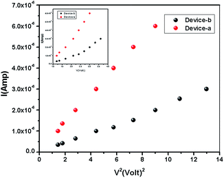
To study the current–voltage (I–V) characteristics, two devices of Al/compound 1/ITO (Device-a) and Al/compound 2/ITO (Device-b) were fabricated. A bias voltage varying from −6 V to +6 V was applied to the devices at room temperature under dark and light condition. The structure of Device-a (or Device-b) is shown on Fig. S1† including the direction of light.
Results and discussion
Structural descriptions of [Cd(adc)(4-phpy)2(H2O)2], (1) and [Zn(adc)(4-phpy)2(H2O)2], (2)
Single crystal X-ray crystallography revealed that both 1 and 2 are isotypical. However, compound 1 crystallizes in the triclinic space group P![[1 with combining macron]](https://www.rsc.org/images/entities/char_0031_0304.gif) with Z = 2. Asymmetric unit in 1 contains distorted octahedral Cd(II) centre ligated by two O atoms from two adc anions in monodentate fashion (Cd–O, 2.289(3)–2.292(3) Å) and two N atoms from two 4-phpy ligands (Cd–N, 2.339(4)–2.343(5) Å) in the equatorial plane, and by O atoms from two aqua ligands at the axial sites (Cd–O, 2.301(3)–2.306(3) Å) (Fig. 1a). The connectivity of the neighboring carboxylate oxygen atoms with Cd(II) centers results in a 1-D coordination polymer. The aqua ligands makes a strong intermolecular hydrogen bond with coordinated O atom of bridging adc ligands with the O⋯O separation of 2.68–2.71 Å (Fig. 1b). In addition, these 1D chains are self-assembled through weak C–H⋯π interactions along the 4-phpy ligands with edge-to-face distances are in the range of 3.306–3.375 Å (Fig. 1c) in ac plane. Thus, 1D zigzag chains aggregate through hydrogen-bonding and C–H⋯π interactions to form a 2D architecture. Moreover, these 1D chains undergo further edge-to-face weak C–H⋯π interactions (3.188–3.506 Å) among the 4-phpy ligands forming 2D network in bc plane (Fig. 1d). These cooperative hydrogen bonding and C–H⋯π interactions (Tables S4 and S5, ESI†) fabricate a 3D supramolecular arrangement by stacking the 1D chains together (Fig. S2, ESI†).
with Z = 2. Asymmetric unit in 1 contains distorted octahedral Cd(II) centre ligated by two O atoms from two adc anions in monodentate fashion (Cd–O, 2.289(3)–2.292(3) Å) and two N atoms from two 4-phpy ligands (Cd–N, 2.339(4)–2.343(5) Å) in the equatorial plane, and by O atoms from two aqua ligands at the axial sites (Cd–O, 2.301(3)–2.306(3) Å) (Fig. 1a). The connectivity of the neighboring carboxylate oxygen atoms with Cd(II) centers results in a 1-D coordination polymer. The aqua ligands makes a strong intermolecular hydrogen bond with coordinated O atom of bridging adc ligands with the O⋯O separation of 2.68–2.71 Å (Fig. 1b). In addition, these 1D chains are self-assembled through weak C–H⋯π interactions along the 4-phpy ligands with edge-to-face distances are in the range of 3.306–3.375 Å (Fig. 1c) in ac plane. Thus, 1D zigzag chains aggregate through hydrogen-bonding and C–H⋯π interactions to form a 2D architecture. Moreover, these 1D chains undergo further edge-to-face weak C–H⋯π interactions (3.188–3.506 Å) among the 4-phpy ligands forming 2D network in bc plane (Fig. 1d). These cooperative hydrogen bonding and C–H⋯π interactions (Tables S4 and S5, ESI†) fabricate a 3D supramolecular arrangement by stacking the 1D chains together (Fig. S2, ESI†).
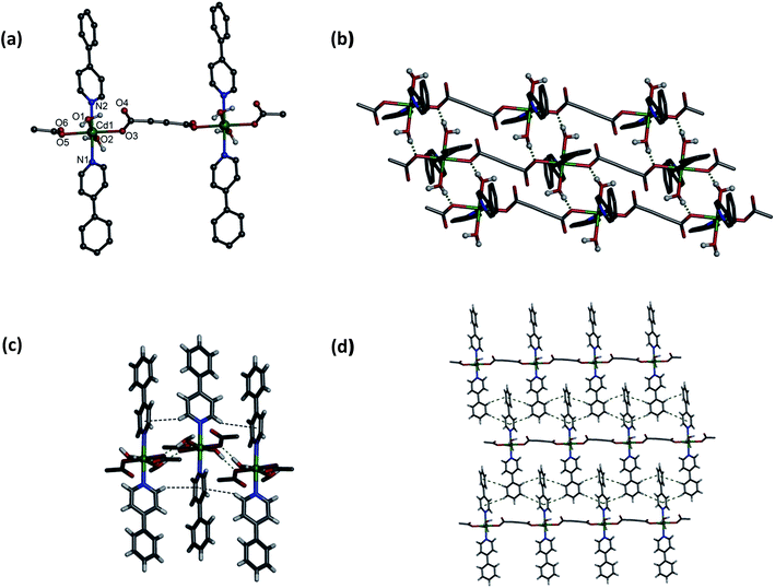 |
| | Fig. 1 (a) A portion of 1D coordination polymer of 1. (b) View of 2D network formed by hydrogen bonding. (c) C–H⋯π interactions in 1 viewed along b-axis. (d) 2D network formed by C–H⋯π interactions by 1D chains viewed along a-axis. | |
On the other hand, compound 2 crystallizes in the monoclinic space group C2/c with Z = 4. Each Zn(II) center in 2 adopts a distorted octahedral geometry and is bonded to two O atoms from two adc anions in monodentate fashion (Zn–O, 2.131(3) Å) and two N atoms from two 4-phpy ligands (Zn–N, 2.139(2)–2.150(3) Å) in the equatorial plane, and by O atoms from two aqua ligands at the axial sites (Zn–O, 2.104(2) Å) (Fig. 4). The bond lengths are comparable to the reported distances in the literatures.39 Overall topology of the compound 2 is isotypical with 1. However, H-bonded O⋯O separation is 2.72 Å in 2, which is little higher than that of 1. Unlike 1, the edge-to-face C–H⋯π distances are symmetrical in both sides of the ring and span in the range of 3.169–3.409 Å. This symmetry has been removed in compound 1.
 |
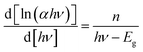
| | Fig. 2 The plot of d[ln(αhν)]/d[hν] versus hν. The plot of ln(αhν) versus ln(hν − Eg) [inset]. | |
 |
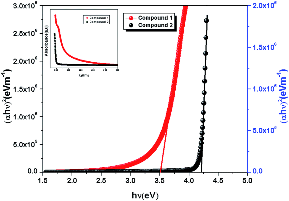
| | Fig. 3 Band gap determination of compound 1 and 2 using Tauc's equation. The absorbance data of 1 and 2 [inset]. | |
 |
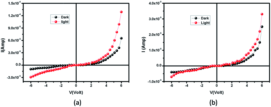
| | Fig. 4 I–V plot under dark and illumination for (a) compound 1 and (b) 2. | |
TGA and PXRD analysis
To check the thermal stability of the compounds, thermogravimetric analyses (TGA) were performed with the powdered sample within the temperature range 30 °C to 600 °C under N2 atmosphere. The results of TGA experiments indicate that the compound 1 is stable upto 100 °C whereas compound 2 is thermally stable upto 140 °C (Fig. S3†). Powder X-ray diffraction (PXRD) has been carried out at room temperature. All of the major peaks of PXRD patterns of as-synthesized 1 and 2 match quite well with those simulated from single crystal data indicating phase purity of the bulk (Fig. S4 and S5†).
Optical characterization
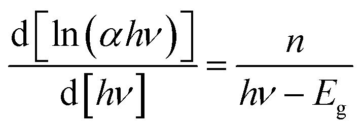
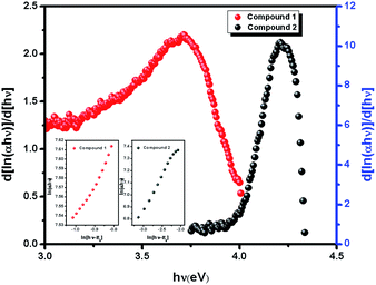
To measure the optical band gap corresponding to the excitation of electron from valance band to conduction band, the optical absorbance spectra of the synthesized materials have been recorded. The optical band gap of the compounds 1 and 2 are calculated using the Tauc's equation.40where α is the absorption coefficient, c is a constant and Eg is the band gap. The value of n may vary for different types of transition. The eqn (1) may be rewritten as:41| |
 | (2) |
In the plot of d[ln(αhν)]/d[hν] versus hν [Fig. 2], a discontinuity is observed. The discontinuity at a particular energy gives the approximate value of band gap. Using the value of approximate band gap (Eg), ln[(αhν)] versus ln[hν − Eg] is plotted [inset of Fig. 2]. The slope of the curve provides the value of n. Here the slope (∼0.5) suggests that the transitions are directly allowed for both the materials. The more accurate band gap of the compounds were calculated by extrapolating the linear portion of (αhν)2 versus hν [Fig. 3]. The value of optical direct band gap of 1 and 2 are evaluated as 3.51 eV and 4.21 eV. Inset of Fig. 3 shows the optical absorbance versus wavelength for the compounds 1 and 2.
Electrical characterization
The current–voltage (I–V) characteristics of compounds 1 and 2 were recorded under dark and illuminated conditions (Fig. 4). In both the conditions, 1 shows higher magnitude of current. At room temperature, the conductivity of 1 under dark and illuminated conditions are calculated as 1.53 × 10⁻⁷ S cm−1 and 3.04 × 10⁻⁷ S cm−1 respectively, whereas the values of these parameters of 2 are 5.90 × 10⁻⁸ S cm−1 and 7.78 × 10⁻⁸ S cm−1 respectively. Interestingly, it has been observed that both the conductivity and photosensitivity are enhanced for 1 in both the conditions. Here, 1 exhibits the photosensitivity of the order of 1.99, which is ∼51% higher than the value, 1.32 obtained in 2.
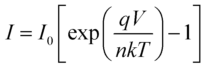
To get better realization of the charge transport mechanism in the device, the thermionic emission (TE) theory is adopted. According to TE theory the current of a diode can be expressed as:42
| |
 | (3) |
where
| |
 | (4) |
here,
I0,
q,
k,
T,
A,
A*,
η and
ϕB stand for the reverse saturation current, electronic charge, Boltzmann constant, temperature in Kelvin, effective diode area (7.065 × 10
−6 m
2), effective Richardson constant (1.20 × 10
6 A m
−2 K
−2), ideality factor and the effective barrier height at zero bias respectively.
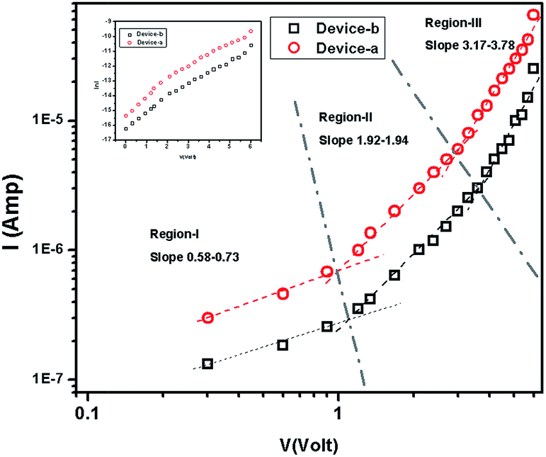
The I–V characteristics of 1 and 2 are presented in Fig. 5. The diverse conduction mechanisms of the devices are obtained from the different regions of the graph. Here Fig. 5 exhibits three different regions under forward bias. The slope of the region-I is less than 1 which is due to ohmic conduction mechanism (I ∝ V) in the low voltage regime. In the region-II, with the slope 1.92–1.94, the conduction mechanism is governed by SCLC mechanism dominated by discrete trapping level (I ∝ V2). The region-III, with the slope 3.17–3.78, is influenced by SCLC mechanism (I ∝ Vn) due to exponential distribution of traps.
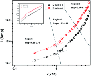 |
| | Fig. 5 Logarithmic plot of I–V characteristics in dark condition for 1 and 2. lnI versus V plot [inset]. | |
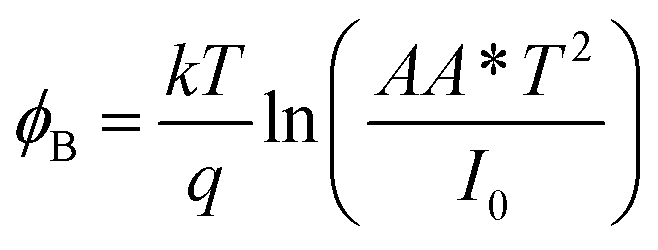
The reverse saturation current is determined from the straight line intercept of lnI–V plot (inset of Fig. 5). The zero bias barrier height is calculated using the following expression.
| |
 | (5) |
The barrier heights of 1 and 2 have been obtained as 0.72 eV and 0.75 eV respectively. Significantly, the lower barrier height of 1 indicates the lower turn-on voltage and higher image force barrier lowering. So the compound 1 is expected to be better candidate for the fast switching device.43
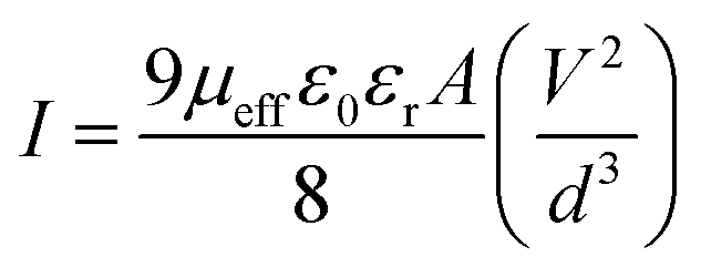
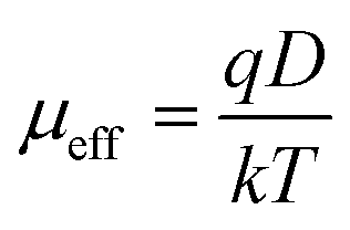
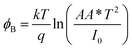
To get the better insight of the charge transport mechanism in the SCLC region (region-II), the effective carrier mobility is estimated from I versus V2 plot (Fig. 6) using the Mott–Gurney equation.44
| |
 | (6) |
where,
ε0 is the free space permittivity,
εr is the dielectric constant of the compounds (10.26 and 5.99 for
1 and
2 respectively),
μeff is the effective mobility of electron and
d is the thickness (∼10 μm) of the thin film. The effective area is assumed as 7.065 × 10
−6 m
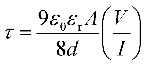
2. The transit time (
τ) of the charge carrier is estimated with the help of following equation [inset of
Fig. 6].
45| |
 | (7) |
 |
| | Fig. 6 I–V2 plot for 1 and 2 in the SCLC region (region-II). I–V plot for determination of the transient time from the SCLC region-II [inset]. | |
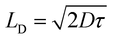
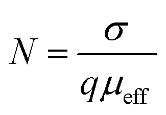
To calculate the diffusion length of charge carrier, Einstein–Smoluchowski equation is used.45
| |
 | (8) |
and
| |
 | (9) |
where,
D is the diffusion co-efficient. The carrier concentration (
Nc) near the junction of the devices
1 and
2 is estimated by using the following equation,
| |
 | (10) |
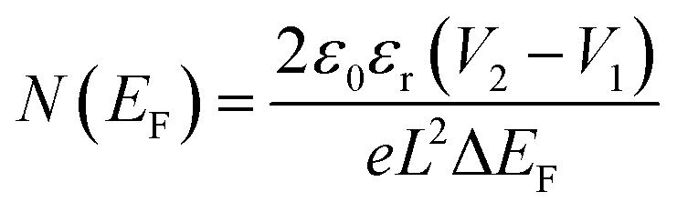
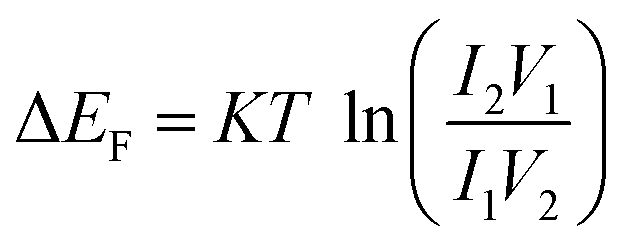
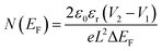
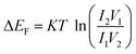
The values of carrier mobility, transient time and diffusion length are summarized in Table 1 with other parameters. It has been observed that the charge carrier mobility of 1 is enhanced up to 68% compared to 2, whereas the diffusion length is increased by 6%. Though the transient time is decreased for 1, but the μτ product is enhanced for 1. The charge carrier for 1 is also enhanced up to 54% compared to 2. The credibility of the compounds depends not only on the charge carrier mobility but also on DOS (density of states) near the Fermi level. The DOS near the Fermi level is determined from the SCLC region of I–V characteristic using den Boer method.46
| |
 | (11) |
where
L is the thickness of the film, Δ
EF is the shift in the quasi-Fermi level,
V1 and
V2 different voltages applied to the diode in the SCLC region (region-II).
| |
 | (12) |
where,
I2 and
I1 are the current values measured at voltages
V2 and
V1 respectively.
Table 1 Comparison of I–V characteristic parameters of 1 and 2
| Sample |
Barrier height |
μeff (m2 V−1 s−1) |
τ (s) |
(μτ) (m2 V−1) |
DOS (V−1 m−3) |
LD (μm) |
Turn on voltage |
SCLC conductivity (S cm−1) |
Nc (m−3) |
| 1 |
0.72 |
9.15 × 10⁻⁷ |
2.63 × 10⁻⁵ |
2.406 × 10⁻¹¹ |
2.576 × 1039 |
1.116 |
0.9746 |
3.885 × 10⁻⁸ |
10.45 × 10¹⁹ |
| 2 |
0.75 |
5.44 × 10⁻⁷ |
3.92 × 10⁻⁵ |
2.132 × 10⁻¹¹ |
3.525 × 1039 |
1.050 |
1.082 |
1.522 × 10⁻⁸ |
6.78 × 10¹⁹ |
Beyond the turn-on voltage, the current increases exponentially with forward bias voltage due to space charge limited conduction (SCLC). Higher number of DOS at Fermi level generally indicates the occurrence of more number of trapping states. More trapping states directly influence the performance of device by degrading its quality. Here the DOS at Fermi level is decreased for 1. Therefore, from all the measured values listed in Table 1, it is very clear that the device fabricated by compound 1 is better than 2. The performance indicating parameters like, mobility, diffusion length, DOS are improved for 1.
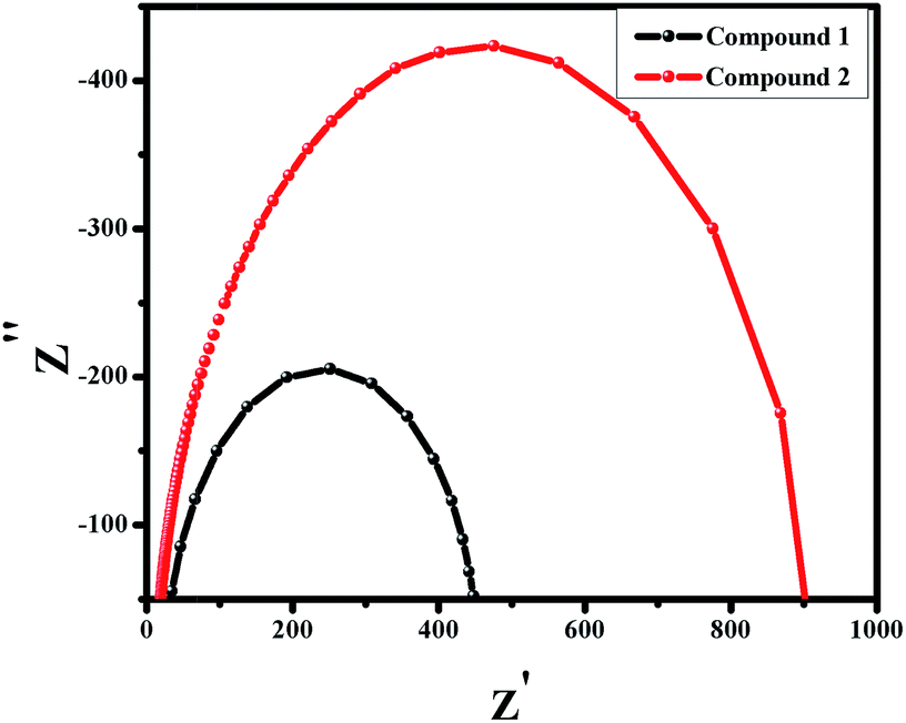
Electrochemical impedance spectroscopy
Electrochemical Impedance spectroscopy (EIS) study is done in the regime of frequency 100 Hz to 1 MHz under 0.5 V bias voltage. Fig. 7 illustrates the nyquist plot of the compounds 1 and 2. It clearly indicates that the semicircle for 1 possesses lesser area than 2. This smaller semicircle depicts the bulk resistance (intercept of semicircle on the Z′ axis) of 1 which is lower than 2. This lower bulk resistance for compound 1 indicates better possibility of charge transfer and reduction of chances of charge recombination.
 |
| | Fig. 7 Nyquist plot for compound 1 and 2. | |
Conclusions
In summary, we have synthesized two 1D coordination polymers from linear dicarboxylate adc by varying metal ion from Cd(II) to Zn(II). The 1D chains herein stack together by the combination of H-bonding and C–H⋯π interactions to form 3D supramolecular structures. These two materials exhibit electrical conductivity and reveal Schottky barrier diode behavior. However, compound 1 shows enhanced photosensitivity, higher mobility, diffusion length and lower DOS at Fermi levels compared to compound 2. Improved charge transport has also been reflected in the device fabricated with 1. Therefore, it appears that compound 1 shows better device applicability compared to 2.
Acknowledgements
This work was supported by SERB, India (Grant No. SB/FT/CS-185/2012) and F. A. thanks UGC, New Delhi, for a Maulana Azad National Fellowship.
References
- S. R. Batten, S. M. Neville and D. R. Turner, Coordination Polymers: Design, Analysis and Application, Royal Society of Chemistry, London, 2009 Search PubMed.
- Design and Construction of Coordination Polymers, ed. M.-C. Hong and L. Chen, John Wiley & Sons, Inc., Hoboken, New Jersey, 2009 Search PubMed.
- Metal–Organic Frameworks. Applications from Catalysis to Gas Storage, ed. D. Farrusseng, Wiley-VCH Verlag GmbH, Weinheim, 2011 Search PubMed.
- G. R. Desiraju, J. J. Vittal and A. Ramanan, Crystal Engineering. A Textbook, World Scientific, Singapore, 2011 Search PubMed.
- A. D. Katsenis, E. K. Brechin and G. S. Papaefstathiou, in Metal–Organic Framework Materials, ed. L. R. MacGillivray and C. M. Lukehart, John Wiley and Sons, UK, 2014 Search PubMed.
- S. Kitagawa, R. Kitaura and S.-I. Noro, Angew. Chem., Int. Ed., 2004, 43, 2334–2375 CrossRef CAS PubMed.
- M. O'Keeffe and O. M. Yaghi, Chem. Rev., 2012, 112, 675–702 CrossRef PubMed.
- J. J. Perry, J. A. Perman and M. J. Zaworotko, Coord. Chem. Rev., 2009, 38, 1400–1417 CAS.
- H.-C. Zhou and S. Kitagawa, Chem. Soc. Rev., 2014, 43, 5415–5418 RSC.
- T. A. Makal, J. Li, W. Lu and H.-C. Zhou, Chem. Soc. Rev., 2014, 43, 5657–5678 RSC.
- J. Duan, M. Higuchi, S. Horike, M. L. Foo, K. P. Rao, Y. Inubushi, T. Fukushima and S. Kitagawa, Adv. Funct. Mater., 2013, 23, 3525–3530 CrossRef CAS.
- H. B. T. Jeazet, C. Staudt and C. Janiak, Dalton Trans., 2012, 41, 14003–14027 RSC.
- Z. Zhang, Y. Zhao, Q. Gong, Z. Li and J. Li, Chem. Commun., 2013, 49, 653–661 RSC.
- B. P. Biswal, H. D. Chaudhari, R. Banerjee and U. K. Kharul, Chem.–Eur. J., 2016, 22, 4695–4699 CrossRef CAS PubMed.
- M. Kurmoo, Chem. Soc. Rev., 2009, 38, 1353–1379 RSC.
- X. Zhang, V. Vieru, X. Feng, J.-L. Liu, Z. Zhang, B. Na, W. Shi, B.-W. Wang, A. K. Powell, L. F. Chibotaru, S. Gao, P. Cheng and J. R. Long, Angew. Chem., Int. Ed., 2015, 54, 9861–9865 CrossRef CAS PubMed.
- D. Aulakh, J. B. Pyser, X. Zhang, A. A. Yakovenko, K. R. Dunbar and M. Wriedt, J. Am. Chem. Soc., 2015, 137, 9254–9257 CrossRef CAS PubMed.
- F.-L. Liu, B. Kozlevčar, P. Strauch, G.-L. Zhuang, L.-Y. Guo, Z. Wang and D. Sun, Chem.–Eur. J., 2015, 21, 18847–18854 CrossRef CAS PubMed.
- Y.-K. Deng, H.-F. Su, J.-H. Xu, W.-G. Wang, M. Kurmoo, S.-C. Lin, Y.-Z. Tan, J. Jia, D. Sun and L.-S. Zheng, J. Am. Chem. Soc., 2016, 138, 1328–1334 CrossRef CAS PubMed.
- J. D. Rocca, D. Liu and W. Lin, Acc. Chem. Res., 2011, 44, 957–968 CrossRef PubMed.
- P. Horcajada, R. Gref, T. Baati, P. K. Allan, G. Maurin, P. Couvreur, G. Féerey, R. E. Morris and C. Serre, Chem. Rev., 2012, 112, 1232–1268 CrossRef CAS PubMed.
- T. Kundu, S. Mitra, P. Patra, A. Goswami, D. Díaz Díaz and R. Banerjee, Chem.–Eur. J., 2014, 20, 10514–10518 CrossRef CAS PubMed.
- A. Corma, H. Garcia and F. X. L. Xamena, Chem. Rev., 2010, 110, 4606–4655 CrossRef CAS PubMed.
- B. Gole, A. K. Bar, A. Mallick, R. Banerjee and P. S. Mukherjee, Chem. Commun., 2013, 49, 7439–7441 RSC.
- Z. Xu, L.-L. Han, G.-L. Zhuang, J. Bai and D. Sun, Inorg. Chem., 2015, 54, 4737–4743 CrossRef CAS PubMed.
- J. Rocha, L. D. Carlos, F. A. A. Paz and D. Ananias, Chem. Soc. Rev., 2011, 40, 926–940 RSC.
- J. Heine and K. Müller-Buschbaum, Chem. Soc. Rev., 2013, 42, 9232–9242 RSC.
- R. Haldar, R. Matsuda, S. Kitagawa, S. J. George and T. K. Maji, Angew. Chem., Int. Ed., 2014, 53, 11772–11777 CrossRef CAS PubMed.
- L. Sun, M. G. Campbell and M. Dincă, Angew. Chem., Int. Ed., 2016, 55, 3566–3579 CrossRef CAS PubMed.
- V. Stavila, A. A. Talin and M. D. Allendorf, Chem. Soc. Rev., 2014, 43, 5994–6010 RSC.
- B. Bhattacharya, A. Layek, M. M. Alam, D. K. Maity, S. Chakrabarti, P. P. Ray and D. Ghoshal, Chem. Commun., 2014, 50, 7858–7861 RSC.
- S. Roy, P. P. Ray, J. Ortega-Castro, A. Frontera and S. Chattopadhyay, Chem. Commun., 2015, 51, 12974–12976 RSC.
- J. L. C. Rowsell and O. M. Yaghi, Microporous Mesoporous Mater., 2004, 73, 3–14 CrossRef CAS.
- N. W. Ockwig, O. Delgado-Friedrichs, M. O'Keeffe and O. M. Yaghi, Acc. Chem. Res., 2005, 38, 176–182 CrossRef CAS PubMed.
- F. Ahmed, S. Roy, K. Naskar, C. Sinha, S. M. Alam, S. Kundu, J. J. Vittal and M. H. Mir, Cryst. Growth Des., 2016, 16, 5514–5519 CAS.
- D. R. Turner, J. Strachan-Hatton and S. R. Batten, CrystEngComm, 2008, 10, 34–38 RSC.
- S. S. Park, E. R. Hontz, L. Sun, C. H. Hendon, A. Walsh, T. Van Voorhis and M. Dincă, J. Am. Chem. Soc., 2015, 137, 1774–1777 CrossRef CAS PubMed.
- G. M. Sheldrick, Acta Crystallogr., Sect. A: Found. Crystallogr., 2008, 64, 112–122 CrossRef CAS PubMed.
- S. Yuan, Y.-K. Deng and D. Sun, Chem.–Eur. J., 2014, 20, 10093–10098 CrossRef CAS PubMed.
- J. Tauc, Amorphous and Liquid Semiconductors, Plenum Press, New York, 1974 Search PubMed.
- F. Yakuphanoglu, B. F. Senkal and A. Sarac, J. Electron. Mater., 2008, 37, 930–934 CrossRef CAS.
- E. H. Rhoderick and R. H. Williams, Metal–Semiconductor Contacts, Clarendon Press, Oxford, 2nd edn, 1988 Search PubMed.
- M. Das, J. Datta, A. Dey, R. Jana, A. Layek, S. Middy and P. P. Ray, RSC Adv., 2015, 5, 101582–101592 RSC.
- M. Soylu and B. Abay, Phys. E, 2010, 43, 534–538 CrossRef CAS.
- A. Dey, A. Layek, A. Roychowdhury, M. Das, J. Datta, S. Middya, D. Das and P. P. Ray, RSC Adv., 2015, 5, 36560–36567 RSC.
- W. den Boer, J. Phys., 1981, 42(C4), 451–454 Search PubMed.
Footnote |
| † Electronic supplementary information (ESI) available: Fig. S1–S2, Tables S1–S5, TGA, PXRD, FTIR and X-ray crystallographic data in CIF format for compounds 1–2. CCDC 1517763 and 1517764. For ESI and crystallographic data in CIF or other electronic format see DOI: 10.1039/c7ra00165g |
|
| This journal is © The Royal Society of Chemistry 2017 |
Click here to see how this site uses Cookies. View our privacy policy here. 
 Open Access Article
 This Open Access Article is licensed under a Creative Commons Attribution-Non Commercial 3.0 Unported Licence
 *b and
Mohammad Hedayetullah Mir
*b and
Mohammad Hedayetullah Mir