
 Open Access Article
 This Open Access Article is licensed under a
 Creative Commons Attribution 3.0 Unported Licence
Rock-salt-type nanoprecipitates lead to high thermoelectric performance in undoped polycrystalline SnSe†
Guodong Tang *a,
Qiang Wena,
Teng Yang*b,
Yang Caoa,
Wei Weia,
Zhihe Wang*c,
Zhidong Zhangb and
Yusheng Lia
*a,
Qiang Wena,
Teng Yang*b,
Yang Caoa,
Wei Weia,
Zhihe Wang*c,
Zhidong Zhangb and
Yusheng Lia
aDepartment of Materials Science and Engineering, Nanjing University of Science and Technology, Nanjing 210094, China. E-mail: tangguodong@njust.edu.cn
bShenyang National Laboratory for Materials Science, Institute of Metal Research, Chinese Academy of Sciences, 72 Wenhua Road, Shenyang 110016, China. E-mail: yangteng@imr.ac.cn
cNational Laboratory of Solid State Microstructures, Department of Physics, Nanjing University, Nanjing 210093, China. E-mail: zhwang@nju.edu.cn
First published on 24th January 2017
Abstract
We report a high ZT value of 1.3 at 850 K for undoped polycrystalline SnSe. The high thermoelectric performance is attributed to a synergistic combination of enhanced power factor and reduction of the lattice thermal conductivity. The presence of rock-salt cubic phase SnSe was identified by X-ray diffraction, transmission electron backscatter diffraction and selected area electron diffraction, which significantly contributes to the enhancement of electrical conductivity and power factor of orthorhombic SnSe material. This new material features a microstructural hierarchy of nanoprecipitates coupled with mesoscale microstructures which leads to a significant reduction of lattice thermal conductivity. As a result, a vast increase in ZT from 0.5 to 1.3 at 850 K was achieved. Our work sheds light on a new mechanism to enhance the thermoelectric properties of SnSe materials.
1. Introduction
As a type of clean energy-conversion system towards a global sustainable energy solution, thermoelectric materials have been the focus of attention. The efficiency of advanced thermoelectric materials is determined by its dimensionless figure of merit (ZT = S2σT/κ, where S, σ, κ, and T are the Seebeck coefficient, electrical conductivity, thermal conductivity, and absolute temperature, respectively). However, the widespread use of thermoelectric technology is constrained by a relatively low conversion efficiency of thermoelectric materials. As such, studies have been conducted to identify and develop new materials with high ZT values.1,2 Several innovative strategies including band engineering,3,4 artificial superlattice structures,5 energy filtering effect,6 and all-scale hierarchical architectures7 have emerged to enhance ZT. Meanwhile, organic polymer thermoelectric materials mainly including conducting polymers8,9 and their composites with inorganic fillers10,11 have sparked intense interest.SnSe, which is made of abundant earth elements, could be the future of low-cost thermoelectric energy generation.12–15 According to the recent work of Zhao et al.,12 SnSe single crystals show high ZT values of 2.6 and 2.3 along b and c axes, respectively, but these crystals yield a significantly reduced ZT value of 0.9 along the a axis at 923 K. Therefore, the thermoelectric properties of SnSe single crystals are highly anisotropic. Moreover, large-scale industrial applications of single-crystals-made thermoelectric devices are prevented by the high cost and big difficulty of single crystal growth. In contrast to single crystals, bulk polycrystalline materials can be easily scaled-up in production lines. However, ZT is very low in undoped polycrystalline SnSe due to its lower electrical conductivity and higher thermal conductivity. For instance, an undoped polycrystalline SnSe was reported to exhibit a very low ZT of 0.5 at about 850 K.16 ZT of ∼0.6 at about 750 K was achieved in Ag doped polycrystalline SnSe by increasing the carrier concentration.17 To facilitate widespread applications, polycrystalline bulk materials that can generate high ZT values must be developed.16–20 Nanostructured engineering has emerged as a promising means to enhance ZT by depressing thermal conductivity through a manipulation of thermal phonons, such as those in LAST1 and BiSbTe.19 The thermoelectric materials fabricated through nanostructured engineering are found to exhibit promising properties for thermoelectric applications.20 Furthermore, preparation cost is considered as another key factor to evaluate thermoelectric materials for practical use. Hydrothermal synthesis is a low-cost and rapid low-temperature method that can be applied to reduce the overall fabrication cost. Here, we used a method which consists of hydrothermal synthesis and spark plasma sintering to produce high-performance undoped polycrystalline SnSe. Interestingly, we found a large amount of cubic rock-salt SnSe phases present in the bulk polycrystalline SnSe material. A high thermoelectric performance ZT value of ∼1.3 at 850 K is achieved in this polycrystalline SnSe material, which is the highest ZT among all undoped polycrystalline SnSe. We demonstrate that the rock-salt-type nanoprecipitates lead to high thermoelectric performance of the polycrystalline SnSe material.
2. Results and discussion
Electron probe micro analyzer (EPMA) was carried out to determine the chemical composition of the sample. The actual chemical composition of the sample before and after SPS is SnSe1.01 and SnSe0.99, respectively. X-ray diffraction (XRD) results (Fig. S1†) indicate the coexistence of Fm![[3 with combining macron]](https://www.rsc.org/images/entities/char_0033_0304.gif) m cubic rock-salt phase and Pnma orthorhombic phase. Besides the pronounced peaks of Pnma orthorhombic phase, the main peaks of the Fmm cubic rock-salt phase can also be found in the XRD patterns. The lattice parameters extracted from the XRD Rietveld refinement are a = 11.51(5), b = 4.14(9), c = 4.45(5) Å and a = 5.89(7) Å for the orthorhombic and cubic rock-salt phases, respectively (Table S1†). To further confirm the existence of Fmm cubic rock-salt phase, we examined the microstructure of the sintered sample using transmission electron backscatter diffraction (t-EBSD). T-EBSD results provide a strong and direct experimental evidence for the existence of new Fmm cubic rock-salt phase (in red in Fig. 1) submerged within the Pnma phase (in blue in Fig. 1). Furthermore, t-EBSD analysis reveals that the relative amount of the cubic phase to the orthorhombic phase is around 25% (Fig. 1). The TEM images of the microstructures of the SnSe material are shown in Fig. 2. Nanoprecipitates in the matrix are clearly found (Fig. 2a and b), which appear as dark quasi-circular (oval) and elongated shape with 10–30 nm in size. Selected area electron diffraction (SAED) pattern was obtained from the marked grain of Fig. 2d. The SAED pattern (Fig. 2c) which consists of Bragg diffraction spots from the cubic rock-salt phase (marked yellow in Fig. 2c) and the Pnma orthorhombic phase (marked red in Fig. 2c) can be observed. Experimental and theoretical studies21,22 have shown that cubic rock-salt SnSe has an almost negligible energy difference from Pnma phase. Possible transition from Pnma to cubic SnSe phase will occur due to a strong correlation between the lattice constants of isostructural and chemically analogous cubic SnSe phase and Pnma phase (Fig. S2†).22 Recent papers showed that the cubic rock-salt SnSe can be induced by microstructure control.23 The size of the precipitated grains could very well play a key parameter in accessing the phase structures which may be kinetically stabilized above a certain size but thermodynamically stabilized below that size.24 Therefore, the size of SnSe nanoscale precipitates ranging from 10 nm to 30 nm is an important parameter to control crystal structure and to produce cubic rock-salt structure SnSe.24
m cubic rock-salt phase and Pnma orthorhombic phase. Besides the pronounced peaks of Pnma orthorhombic phase, the main peaks of the Fmm cubic rock-salt phase can also be found in the XRD patterns. The lattice parameters extracted from the XRD Rietveld refinement are a = 11.51(5), b = 4.14(9), c = 4.45(5) Å and a = 5.89(7) Å for the orthorhombic and cubic rock-salt phases, respectively (Table S1†). To further confirm the existence of Fmm cubic rock-salt phase, we examined the microstructure of the sintered sample using transmission electron backscatter diffraction (t-EBSD). T-EBSD results provide a strong and direct experimental evidence for the existence of new Fmm cubic rock-salt phase (in red in Fig. 1) submerged within the Pnma phase (in blue in Fig. 1). Furthermore, t-EBSD analysis reveals that the relative amount of the cubic phase to the orthorhombic phase is around 25% (Fig. 1). The TEM images of the microstructures of the SnSe material are shown in Fig. 2. Nanoprecipitates in the matrix are clearly found (Fig. 2a and b), which appear as dark quasi-circular (oval) and elongated shape with 10–30 nm in size. Selected area electron diffraction (SAED) pattern was obtained from the marked grain of Fig. 2d. The SAED pattern (Fig. 2c) which consists of Bragg diffraction spots from the cubic rock-salt phase (marked yellow in Fig. 2c) and the Pnma orthorhombic phase (marked red in Fig. 2c) can be observed. Experimental and theoretical studies21,22 have shown that cubic rock-salt SnSe has an almost negligible energy difference from Pnma phase. Possible transition from Pnma to cubic SnSe phase will occur due to a strong correlation between the lattice constants of isostructural and chemically analogous cubic SnSe phase and Pnma phase (Fig. S2†).22 Recent papers showed that the cubic rock-salt SnSe can be induced by microstructure control.23 The size of the precipitated grains could very well play a key parameter in accessing the phase structures which may be kinetically stabilized above a certain size but thermodynamically stabilized below that size.24 Therefore, the size of SnSe nanoscale precipitates ranging from 10 nm to 30 nm is an important parameter to control crystal structure and to produce cubic rock-salt structure SnSe.24
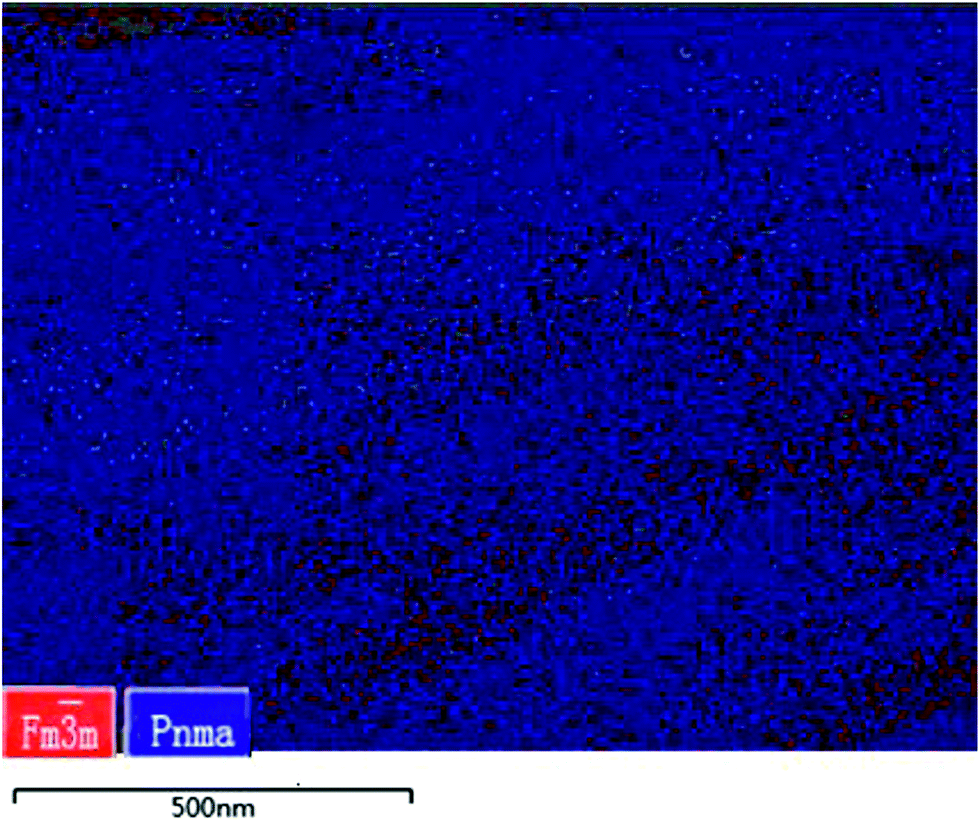 | ||
| Fig. 1 Phase map of polycrystalline SnSe with grains identified as Fmm cubic rock-salt phase in red and Pnma orthorhombic phases in blue from t-EBSD measurements. | ||
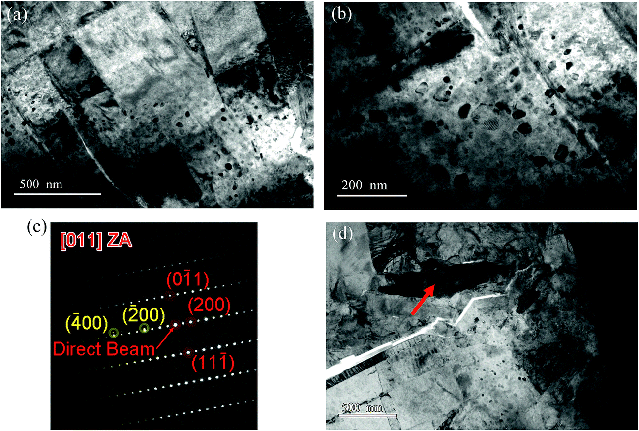 | ||
| Fig. 2 Microstructures of polycrystalline SnSe. (a) Low-magnification TEM image. (b) Medium-magnification TEM images. (c) The SAED pattern measured on the marked grain shown in (d), revealing the coexistence of cubic rock-salt phase (in yellow) and orthorhombic phase (in red). (d) TEM image revealing mesoscale grains. | ||
The curves of Seebeck coefficient (S) measured along the pressing direction are shown in Fig. 3a. S is positive and consistent with Hall measurements for p-type SnSe. The values of the current sample are lower than those observed in bulk polycrystalline SnSe and SnSe single crystals. This result can be attributed to the increase in carrier concentration identified by Hall measurements. S increases as temperature increases, reaching a maximum value at approximately 650 K. Seebeck coefficient peak is a sign of bipolar conduction onset. A slight structural change25 causes bipolar conduction as the temperature increases. The absolute value of S decreases, when the temperature reaches the intrinsic range of this material. At the intrinsic range of the temperature, the thermal excited electrons transfer from the valence band to the conduction band; in this manner, the same number of holes is produced. The contribution of a minority carrier adversely affects S. Compared with that of the SnSe single crystals, Seebeck coefficient peak of the current sample shifts to a higher temperature. The upturn of S above 800 K is related to the structural transition from Pnma to Cmcm.12,16 A structural transition from Pnma to Cmcm occurs at about 793 K, as indicated by the temperature dependence of specific heat for SnSe polycrystals in Fig. S3.†
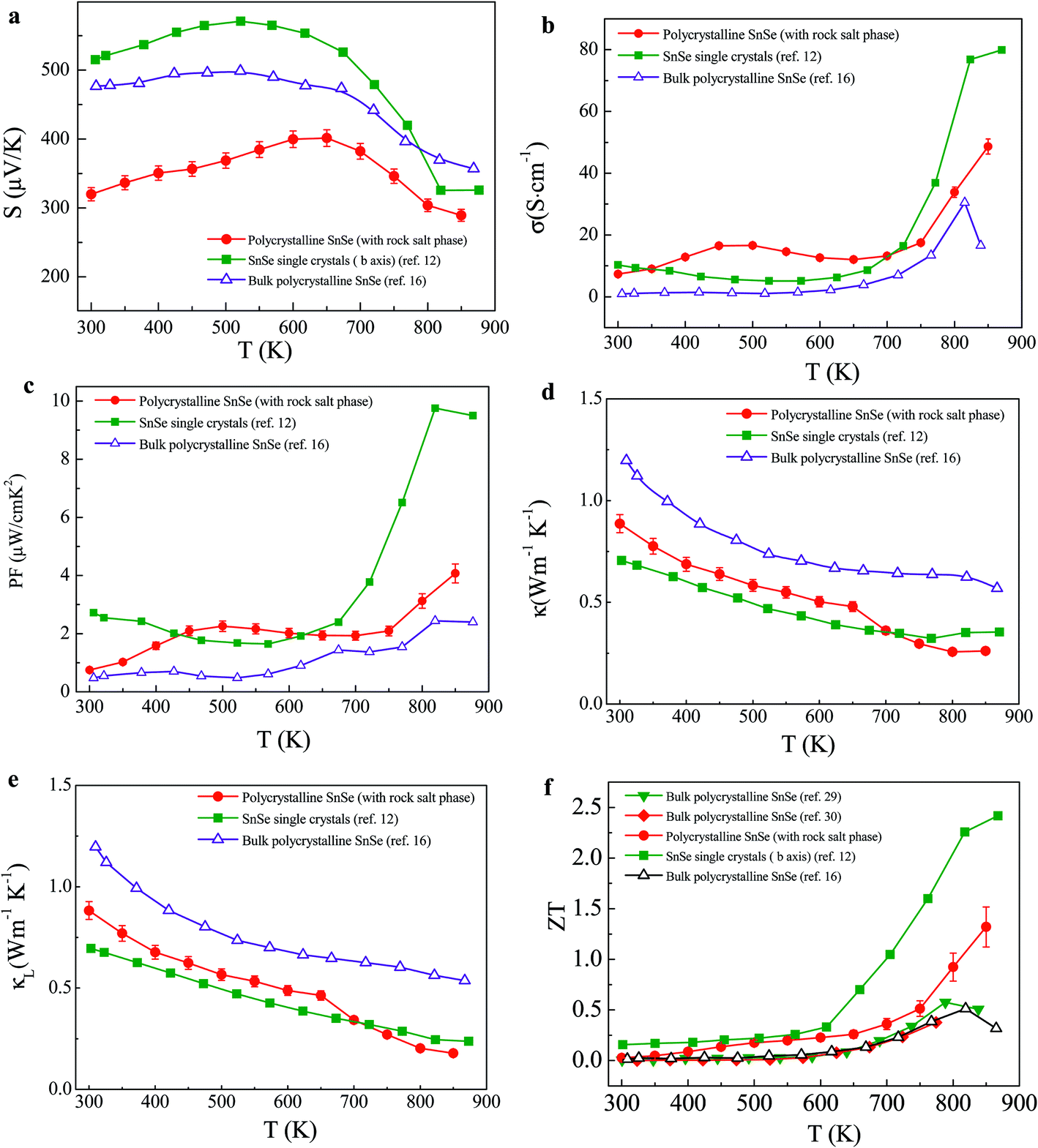 | ||
| Fig. 3 Temperature dependence of (a) Seebeck coefficient, (b) electrical conductivity; the inset is enlarged σ, (c) power factor, (d) total thermal conductivity, (e) lattice thermal conductivity, (f) ZT for polycrystalline SnSe measured along the pressing direction. | ||
Fig. 3b shows the temperature dependence of electrical conductivity σ of the polycrystalline SnSe material measured along the pressing direction. The data were compared with those previously reported in the bulk polycrystalline SnSe and SnSe single crystals. The behavior of electrical transport of this sample can be described as follows: a semiconducting transport behavior occurs from 300 K to 450 K; then changes to metallic-like behavior up to 650 K; and finally increases until 850 K. An increase in σ from 650 K to 850 K can be attributed to thermal excitation of carriers. σ of bulk polycrystalline SnSe previously reported16 is 0.9 S cm−1 at room temperature; this value increases to 16.5 S cm−1 at 840 K. Our polycrystalline SnSe typically exhibit a room-temperature electrical conductivity value of σ = 7.3 S cm−1, which increases to 48.6 S cm−1 at 850 K. The results demonstrate that σ obtained in our polycrystalline SnSe is significantly larger than those reported in other polycrystalline SnSe. Our theoretical calculation (see ESI†) shows that the Fmm phase has a much better electrical conductivity than the Pnma phase. T-EBSD analysis reveals that the islands of new cubic rock-salt phase (in red in Fig. 1) permeate through the Pnma matrix phase and it is reasonable to treat the two-phase composite as a percolation conduction network.26,27 According to the percolation model,26,27 one phase (Fmm) which has a relatively high electrical conductivity and a considerable amount of dispersion in a low-conductivity matrix (Pnma) can contribute to an improvement on the electrical conductivity of the Pnma matrix phase. Of course we should take into account the presence of numerous interfaces in the material which scatters carriers and impairs carrier mobility. Whether or not the interface carrier scattering can compromise the positive contribution of the cubic phase depends on the competition between carrier concentration and mobility.28 We believe that the σ enhancement due to the increased carrier concentration can surpass the reduction of carrier mobility due to the interface scattering. This can find some support from the followings: (1) the calculated electronic band structure in Fig. S4 in the ESI† shows that the band gap of the cubic phase is around 0.22 eV (in contrast to 0.61 eV of the orthorhombic phase), and the smaller the band gap, the larger the number of thermally activated carriers; (2) a large electronic density of states, which can be found in the cubic phase near the top/bottom of valence/conduction band due to band inversion induced by spin orbit coupling, can give rise to a big carrier concentration n. (3) This is also supported by the enhanced carrier concentration identified by our Hall measurements. The room-temperature carrier concentration is 5.6 × 10¹⁸ holes per cm3 for the polycrystalline SnSe material, which is larger by one order of magnitude than that of the reported polycrystalline bulk SnSe (∼4 × 10¹⁷ holes per cm3)16 and single crystals (∼4 × 10¹⁷ holes per cm3).12 Therefore, the introduction of cubic phase contributes to the improvement of electrical conductivity of orthorhombic SnSe material. As shown in Fig. 3b, σ of the polycrystalline SnSe material containing cubic rock-salt precipitates is enhanced upon that of the previously reported polycrystalline materials.16 The rock-salt phases lead to high electrical conductivity and ultimately contribute to the enhanced PF, in consistent with what's observed in Fig. 3c.
The temperature dependence of total thermal conductivity (κ) measured along the pressing direction is presented and compared with that of other polycrystalline materials16 and single crystals12 in Fig. 3d. A general and expected trend found for three kinds of materials is that κ drops with rising temperature. For the polycrystalline SnSe, it is shown in Fig. 3d that κ is comparable to the ultralow thermal conductivity of single crystals at the temperature below 700 K, and even lies below the κ of the single crystals above 700 K. For example, κ dropping from 0.88 W m−1 K−1 at 300 K to 0.26 W m−1 K−1 at 850 K was observed in our polycrystalline SnSe, in contrast to κ decreasing from 0.70 to 0.35 W m−1 K−1 in single crystals. The kink at around 650 K is related to the slight structural change.25 The extraordinarily low κ of the SnSe nanocrystals (0.26 W m−1 K−1), together with the enhancement of both electrical conductivity and PF due to the presence of Fmm cubic rocksalt phase, helps achieve high ZT in undoped polycrystalline SnSe. To comprehend the ultralow κ of the SnSe polycrystals, we calculated lattice thermal conductivity (κL) by first estimating carrier counterpart κe based on the Wiedeman–Franz law (κe = LT/ρ, L = 2.0 × 10⁻⁸ V2 K−2) and then subtracting κe from total thermal conductivity, namely, κL = κ − κe. The negligible difference between the total thermal conductivity κ and the lattice counterpart κL reveals that phonon transport dominates in κ (Fig. 3e). Compared with previously reported polycrystalline SnSe, κL of our polycrystalline SnSe is significantly reduced. The very large reductions in κL of our polycrystalline SnSe can be explained by the hierarchical microstructure consisting nanoprecipitates and mesoscale matrix grains. Nanoprecipitates are clearly evidenced in the TEM images (Fig. 2a and b). Besides nanoprecipitates, the presence of mesoscale grains (0.1–1.8 μm in size) is evident in Fig. 2a and d. In addition, SnSe exhibits intrinsically low thermal conductivity due to strong phonon anharmonicity.29 Therefore, nanoprecipitates combined with long-wavelength phonon scattering centers (mesoscale grains), and short-wavelength phonon scattering centers (an outcome of anharmonicity of chemical bonds in SnSe), define all-hierarchical architectures to scatter phonons. Therefore, a significant reduction of κL was obtained in the present undoped polycrystalline SnSe.
ZT as a function of temperature in our polycrystalline SnSe along the pressing direction is compared to those of both polycrystalline and SnSe single crystals previously reported (Fig. 3f). ZT values of our polycrystalline SnSe are lower than that of SnSe single crystals in the investigated temperature range,12 but significantly larger than those of previously reported SnSe polycrystalline materials.16,30,31 A vast increase of ZT from 0.5 to 1.3 at 850 K was achieved in our undoped polycrystalline SnSe along the pressing direction. Thermoelectric performance of our polycrystalline SnSe is much improved upon that of polycrystalline SnSe previously reported by others, mainly due to the rock-salt-type cubic nanoprecipitates newly identified in our polycrystalline SnSe material. This new phase significantly contributes to the enhancement of electrical conductivity and power factor of orthorhombic SnSe material. Our new polycrystalline material features a microstructural hierarchy of nanoprecipitates coupled with mesoscale microstructures which leads to significant reduction of lattice thermal conductivity. Good experimental repeatability for the high ZT was obtained, as evidenced by the measurements on several independently prepared samples (Fig. S6†).
Bulk polycrystalline SnSe shows anisotropy in their transport properties due to the anisotropic crystal structure of this compound.18 Our polycrystalline SnSe shows similar anisotropic transport properties. Fig. 4 shows the thermoelectric properties measured perpendicular to the pressing direction. The Seebeck coefficient, electrical conductivity, and thermal conductivity show obvious anisotropy (Fig. 4a–c). σ is higher perpendicular to the pressing direction than that along the pressing direction. However, ZT (Fig. 4d) along the pressing direction is a litter bit higher due to a much lower thermal conductivity, consistent with the previously reported polycrystalline SnSe doped with Ag.17
 | ||
| Fig. 4 Temperature dependence of (a) Seebeck coefficient, (b) electrical conductivity, (c) thermal conductivity, (d) ZT for polycrystalline SnSe perpendicular to the pressing direction (⊥). | ||
3. Conclusions
In summary, we have successfully fabricated high-performance polycrystalline SnSe materials by facile hydrothermal synthesis. We demonstrate that the presence of cubic rock-salt-type precipitate phase contributes significantly to the enhancement of both electrical conductivity and PF of the SnSe material. Nanoprecipitates coupled with mesoscale matrix grains lead to significant reduction of lattice thermal conductivity through hierarchical architecturing. The simultaneous optimization of both PF and lattice thermal conductivity help achieve remarkably high thermoelectric performance ZT of ∼1.3 at 850 K.4. Experimental section
Polycrystalline SnSe was synthesized using hydrothermal methods. SnCl2·2H2O (1.4 g) was first dissolved in 50 ml deionized water. The solution was then sonicated at room temperature for 10 min, followed by addition of 90 milllimoles of NaOH and sonicated for another 10 min. The mixture was then transferred to a Teflon-lined stainless steel autoclave of 100 ml capacity followed by the addition of 0.24 g Se, and then heated at 403 K for 36 h. After cooling to room temperature, the products were collected and thoroughly washed with absolute ethanol and deionized water for several times. The powders were dried at 333 K for 4 h with a vacuum dryer. The above steps were repeated to obtain more dried powders. The dried powders were loaded in a graphite die of 10 mm in diameter, then densified by spark plasma sintering at 693 K for 7 min under a uniaxial pressure of 50 MPa.The powder X-ray diffraction patterns were performed on a Bruker D8 Advance instrument with Cu Kα radiation (λ = 1.54060 Å) and scanning with a step size of 0.02°. Chemical composition of the sample was determined by electron probe micro analysis (EPMA). Transmission electron microscopy (TEM) investigations were conducted with a JEOL 2100F microscope and a FEI Tecnai 20 microscope; both were operated at 200 kV acceleration voltage. We prepared TEM samples by conventional standard methods. The preparation is accomplished by ion milling using a precision ion polishing system (PIPS, Model 691, Gatan, USA). T-EBSD measurements were performed on a Zeiss Auriga field emission scanning electron microscope equipped with a Nordlys-Nano EBSD detector. An accelerating voltage of 30 keV was used with a probe current of 1.6 nA and a step size of 4 nm. Sample was prepared for t-EBSD analysis by focused ion beam (FIB) milling using the in situ lift-out technique on a FEI Nova Nanolab DualBeam instrument.
The obtained SPS processed pellets were cut into bars with dimensionless of 10 × 3 × 3 mm. These bars were used for simultaneous measurements of the Seebeck coefficient and electrical conductivity using an Ulvac-Riko ZEM-3 instrument system under a helium atmosphere in the temperature range of 300–850 K. Electrical properties obtained from several independently prepared samples were similar. The thermal diffusivity coefficient D was measured at 300–850 K by the laser flash diffusivity method in a Netzsch LFA-457 instrument. The thermal diffusivity measurements were performed on coins of ϕ 6 mm and 1–2 mm thickness. The heat capacity Cp was measured using differential scanning calorimeter (DSC). The density ρ was determined using the dimensions and mass of the sample, and then reconfirmed using the Archimedes method. The thermal conductivity was calculated from κ = DCpρ. Thermal conductivities obtained from several independently prepared samples were similar. The Hall coefficient (RH) was determined using a physical properties measurement system. The carrier concentration (n) was calculated by using n = 1/eRH, where e is the electronic charge. The uncertainty for the electrical conductivity is 5%, the Seebeck coefficient 3%, the thermal conductivity 5%. The combined uncertainty for all measurements involved in the calculation of ZT is around 15%.
Acknowledgements
This work was supported by the National Natural Science Foundation of China (11204134), and Natural Science Foundation of Jiangsu Province (BK20161495). T. Y. and Z. D. Z. acknowledge the Major Program of Aerospace Advanced Manufacturing Technology Research Foundation NSFC and CASC, China (No. U1537204) and NSFC under Grant No. 51331006 for the financial support.Notes and references
- K. F. Hsu, S. Loo, F. Guo, W. Chen, J. S. Dyck, C. Uher, T. Hogan, E. K. Polychroniadis and M. G. Kanatzidis, Science, 2004, 303, 818 CrossRef CAS PubMed.
- L. D. Zhao, V. P. Dravid and M. G. Kanatzidis, Energy Environ. Sci., 2014, 7, 251 CAS.
- J. P. Heremans, V. Jovovic, E. S. Toberer, A. Saramat, K. Kurosaki, A. Charoenphakdee, S. Yamanaka and G. J. Snyder, Science, 2008, 321, 554 CrossRef CAS PubMed.
- Y. Z. Pei, X. Y. Shi, A. LaLonde, H. Wang, L. D. Chen and G. J. Snyder, Nature, 2011, 473, 66 CrossRef CAS PubMed.
- R. Venkatasubramanian, E. Siivola, T. Colpitts and B. O'Quinn, Nature, 2001, 413, 597 CrossRef CAS PubMed.
- J. P. Heremans, C. M. Thrush and D. T. Morelli, Phys. Rev. B: Condens. Matter Mater. Phys., 2004, 70, 115334 CrossRef.
- K. Biswas, J. Q. He, I. D. Blum, C. I. Wu, T. P. Hogan, D. N. Seidman, V. P. Dravid and M. G. Kanatzidis, Nature, 2012, 489, 414 CrossRef CAS PubMed.
- O. Bubnova, Z. U. Khan, A. Malti, S. Braun, M. Fahlman, M. Berggren and X. Crispin, Nat. Mater., 2011, 10, 429 CrossRef CAS PubMed.
- X. Hu, G. Chen, X. Wang and H. Wang, J. Mater. Chem. A, 2015, 3, 20896 CAS.
- L. Liang, C. Gao, G. Chen and C.-Y. Guo, J. Mater. Chem. C, 2016, 4, 526 RSC.
- C. Gao and G. Chen, Compos. Sci. Technol., 2016, 124, 52 CrossRef CAS.
- L. D. Zhao, S. H. Lo, Y. S. Zhang, H. Sun, G. J. Tan, C. Uher, C. Wolverton, V. P. Dravid and M. G. Kanatzidis, Nature, 2014, 508, 373 CrossRef CAS PubMed.
- L. D. Zhao, G. J. Tan, S. Q. Hao, J. Q. He, Y. L. Pei, H. Chi, H. Wang, S. K. Gong, H. B. Xu, V. P. Dravid, C. Uher, G. J. Snyder, C. Wolverton and M. G. Kanatzidis, Science, 2016, 351, 141 CrossRef CAS PubMed.
- K. L. Peng, X. Lu, H. Zhan, S. Hui, X. D. Tang, G. W. Wang, J. Y. Dai, C. Uher, G. Y. Wang and X. Y. Zhou, Energy Environ. Sci., 2016, 9, 454 CAS.
- G. D. Tang, W. Wei, J. Zhang, Y. S. Li, X. Wang, G. Z. Xu, C. Chang, Z. H. Wang, Y. W. Du and L. D. Zhao, J. Am. Chem. Soc., 2016, 138, 13647 CrossRef CAS PubMed.
- S. Sassi, C. Candolfi, J. B. Vaney, V. Ohorodniichuk, P. Masschelein, A. Dauscher and B. Lenoir, Appl. Phys. Lett., 2014, 104, 212105 CrossRef.
- C. L. Chen, H. Wang, Y. Y. Chen, T. Day and G. J. Snyder, J. Mater. Chem. A, 2014, 2, 11171 CAS.
- Q. Zhang, E. K. Chere, J. Y. Sun, F. Cao, K. Dahal, S. Chen, G. Chen and Z. F. Ren, Adv. Energy Mater., 2015, 5, 1500360 CrossRef.
- B. Poudel, Q. Hao, Y. Ma, Y. C. Lan, A. Minnich, B. Yu, X. Yan, D. Z. Wang, A. Muto, D. Vashaee, X. Y. Chen, J. M. Liu, M. S. Dresselhaus, G. Chen and Z. F. Ren, Science, 2008, 320, 634 CrossRef CAS PubMed.
- M. S. Dresselhaus, G. Chen, M. Y. Tang, R. Yang, H. Lee, D. Z. Wang, Z. F. Ren, J. P. Fleurial and P. Gogna, Adv. Mater., 2007, 19, 1043 CrossRef CAS.
- Y. Sun, Z. C. Zhong, T. Shirakawa, C. Franchini, D. Z. Li, Y. Y. Li, S. Yunoki and X. Q. Chen, Phys. Rev. B: Condens. Matter Mater. Phys., 2013, 88, 235122 CrossRef.
- A. N. Mariano and K. L. Chopra, Appl. Phys. Lett., 1967, 10, 282 CrossRef CAS.
- Z. Y. Wang, J. F. Wang, Y. J. Zang, Q. H. Zhang, J. A. Shi, T. Jiang, Y. Gong, C. L. Song, S. H. Ji, L. L. Wang, L. Gu, K. He, W. H. Duan, X. Ma, X. Chen and Q. K. Xue, Adv. Mater., 2015, 27, 4150 CrossRef CAS PubMed.
- R. B. Soriano, J. S. Wu and M. G. Kanatzidis, J. Am. Chem. Soc., 2015, 137, 9937 CrossRef CAS PubMed.
- K. Adouby, C. Perez-Vicente, J. C. Jumas and R. Fourcade, Z. Kristallogr., 1998, 213, 343 CAS.
- S. Kirkpatrick, Rev. Mod. Phys., 1973, 45, 574 CrossRef.
- D. S. McLachlan, M. Blaszkiewicz and R. E. Newnham, J. Am. Ceram. Soc., 1990, 73, 2187 CrossRef CAS.
- J. M. Ziman, Principles of the Theory of Solids, Cambridge University Press, Cambridge, England, 2nd edn, 1995 Search PubMed.
- C. W. Li, J. Hong, A. F. May, D. Bansal, S. Chi, T. Hong, G. Ehlers and O. Delaire, Nat. Phys., 2015, 11, 1063 CrossRef CAS.
- Y. L. Li, X. Shi, D. D. Ren, J. K. Chen and L. D. Chen, Energies, 2015, 8, 6275 CrossRef CAS.
- T. R. Wei, C. F. Wu, X. Z. Zhang, Q. Tan, L. Sun, Y. Pan and J. F. Li, Phys. Chem. Chem. Phys., 2015, 17, 30102 RSC.
Footnote |
| † Electronic supplementary information (ESI) available. See DOI: 10.1039/c7ra00140a |
| This journal is © The Royal Society of Chemistry 2017 |