DOI:
10.1039/C7RA00066A
(Paper)
RSC Adv., 2017,
7, 20732-20737
A contact study in hole conductor free perovskite solar cells with low temperature processed carbon electrodes†
Received
3rd January 2017
, Accepted 4th April 2017
First published on 11th April 2017
Abstract
Hole conductor material (HTM) free photovoltaic devices with graphite electrodes were fabricated at low temperature. An FTO/perovskite contact and TiO2/graphite contact were investigated. The results suggest that the carrier recombination processes resulting from FTO/perovskite and TiO2/carbon contacts affect the device performance greatly. By optimization, a 65 nm TiO2 compact layer with a 380 nm TiO2 mesoporous layer can efficiently decrease the contact between FTO and perovskite materials. The contact between TiO2 and graphite was lowered by the improvement of perovskite coverage. The photo-voltages were enhanced from 0.695 V to 0.820 V and a best efficiency of 10.4% was obtained.
Introduction
Being renewable and clean, solar energy is very promising to substitute fossil energy in the future. Photovoltaic devices can be used to convert solar energy to electricity directly. A low cost and high photo-electrical conversion efficiency (PCE) has always been the goal for photovoltaic device research. Perovskite solar cells (PSCs) based on mixed organic–inorganic halide perovskites ABX3 (A = CH3NH3 (MA) or NH2CHNH2 (FA), B = Pb or Sn, X = Cl, Br, I or mixed halides) were just in line with the requirements of low cost and high efficiency, and have attracted a lot of attention from scientists all around the world since 2009.1–16 At this point in time, PSCs have reached an efficiency of over 20%.2
Perovskite photovoltaic devices were based on the structure of dye sensitized solar cells at first,3–6 then it was found that perovskite can act as both an electron and hole transport layer itself, and devices based on a planar structure appeared.7–13 In these structures, TCO and HTM are the most expensive components14 and the HTM layer is even less conductive than perovskite materials themselves. For these reasons, some scientists tried to use carbon-based materials to dope or replace the HTMs.15,16 Moreover, other researchers turned their attention toward TCO free17–19 and HTM free20–37 perovskite solar cells.
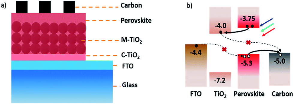
In HTM free structure, graphite materials were often used as counter electrodes because as a resource they were easily accessible, cheap and stable.24–37 Han's group have carried out some pioneering work with graphite electrodes,28–31 adopting a high temperature (400 °C) processed graphite electrode and then dipping perovskite materials into the device. In order to reduce electrical leakage, a thick barrier layer (1 μm ZrO2) was introduced on the TiO2 mesoporous layer. The device efficiency of this structure has reached to about 15%.33 However, the thick barrier layer (ZrO2, Al2O3, etc.) in this structure may introduce a high series resistance, some scientists were then focused on devices without the thick barrier layers. To solve the electrical leakage problem, low temperature processed graphite electrodes were introduced in the new structure which could then be printed after the perovskite was loaded into TiO2,35–37 so that finally an efficiency of 13.5% was obtained.37 The HTM free PSCs device structure with low temperature processed graphite electrodes is illustrated in Fig. 1a. Fig. 1b is the corresponding energy band diagram. The carrier transport processes show that photo-induced carriers can be separated by perovskite/TiO2 heterojunction but might be recombined at FTO/perovskite and TiO2/carbon contact area, which may affect the device performance greatly. However, there were few research papers reporting the contact effects on performances of HTM free PSCs.
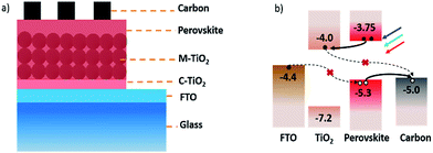 |
| | Fig. 1 (a) A schematic structure of the perovskite solar cell device and (b) the corresponding energy band diagram and the carrier transport process. | |
Here, we fabricated HTM free perovskite solar cells with low temperature graphite electrodes. We then investigated the effects of FTO/perovskite and TiO2/graphite contacts on the device's performances. By optimization, the photo-voltage was improved from 0.695 V to 0.820 V with an improvement of 18% and an efficiency of 10.4% was finally obtained.
Experimental section
Materials
All reagents and solvents were used as received. Tetrabutyltitanate, anhydrous ethanol, diethanolamine, TiO2 paste (Dyesol 18NRT), PbCl2 (99.999%, Alfa Aesar), CH3NH3I (99.9%, HeptaChroma), anhydrous N′,N-dimethylformamide (DMF, 99.8%, Super Dry, J&K), graphite paste (Guangzhou Seaside Technology Co., Ltd), FTO glasses (8 Ω □−1, HeptaChroma).
Preparation of TiO2 layers
FTO glasses was sonically cleaned by acetone, ethanol and deionized water for 15 minutes, respectively, after dried by nitrogen gun, the FTO glasses were treated by UV-O3 for 15 minutes. The TiO2 compact precursor dispersion was prepared by mixing 22.6909 g tetrabutyltitanate, 89.068 g anhydrous ethanol, 2.8 g deionised water and 7.01 g diethanolamine together and stirring for 24 hours. We then let the dispersion stand for 24 hours. Then the dispersion was spin-coated on FTO at different speed (4000, 5000, 6000, 7000, 8000 rpm) and heated in an oven at 500 °C for 2 hours (the heating rate was 2 °C min−1). After they had cooled down to room temperature, mesoporous TiO2 layer was deposited on the substrates by spin-coating a commercial TiO2 paste (Dyesol 18NRT, Dyesol) diluted in ethanol (1 g TiO2 paste in 3.5 g ethanol) at various speed (1500, 2000, 3000, 4000, 6000 rpm) and finally heated in an oven at 500 °C for 30 minutes (the heating rate was 2 °C min−1).
Fabrication of photovoltaic devices
The perovskite precursor solution with different concentrations (13.2 wt%, 26.4 wt%, 44.3 wt%, 51.5 wt%) were made by dissolving CH3NH3I and PbCl2 (3![[thin space (1/6-em)]](https://www.rsc.org/images/entities/char_2009.gif) :1 M ratio) into DMF, which were stirred at 60 °C overnight. For instance, 51.5 wt% solution contains 0.636 g CH3NH3I and 0.371 g PbCl2 in 1 ml DMF. After the solution cooled to room temperature, the solution was filtered twice using a 0.45 μm pore PVDF syringe filter. Then the solution was spin-coated on TiO2 substrate at a speed of 3000 rpm for 30 s and then heated at 110 °C for 45 minutes on a hotplate, all these process was carried out under Ar atmosphere (O2 and H2O <1 ppm). After that, the samples were taken out to ambient atmosphere and a layer of graphite paste was quickly printed on perovskite layer by doctor-blading method, which is heated at 100 °C for 15 minutes then. The thickness of graphite electrodes were controlled by using a 10 μm thick tape. Then they were heated at 100 °C for 15 minutes on a hotplate. Finally the electrodes were extracted by pressing copper tapes on graphite with clamps.
:1 M ratio) into DMF, which were stirred at 60 °C overnight. For instance, 51.5 wt% solution contains 0.636 g CH3NH3I and 0.371 g PbCl2 in 1 ml DMF. After the solution cooled to room temperature, the solution was filtered twice using a 0.45 μm pore PVDF syringe filter. Then the solution was spin-coated on TiO2 substrate at a speed of 3000 rpm for 30 s and then heated at 110 °C for 45 minutes on a hotplate, all these process was carried out under Ar atmosphere (O2 and H2O <1 ppm). After that, the samples were taken out to ambient atmosphere and a layer of graphite paste was quickly printed on perovskite layer by doctor-blading method, which is heated at 100 °C for 15 minutes then. The thickness of graphite electrodes were controlled by using a 10 μm thick tape. Then they were heated at 100 °C for 15 minutes on a hotplate. Finally the electrodes were extracted by pressing copper tapes on graphite with clamps.
Characterization
A field-emission scanning electron micrograph (SEM) at an acceleration voltage of 20 kV were used to characterize the surface morphology of perovskite film and thickness of TiO2 film (FEI Quanta 600 microscope). X-ray diffraction patterns were carried out by a Bruker-AXS Micro diffractometer (model D5005). UV-vis transmittance spectra were recorded by an UV-vis Spectrophotometer and the wavelength varied from 350 nm to 800 nm (UV 5000 spectrometer, Cary). J–V curves and the stabilized-power output curve were measured by an electrochemical workstation (CHI660c) under 100 mW cm−2 illumination (AM 1.5 G) by a solar simulator (300 W Oriel Solar Simulator Model, 91160). For the J–V measurement, the voltage step and scan rate were 1 mV and 0.1 V s−1, respectively. The backward scanning started from −1 V (over the open-circuit photo voltage) to 0 V (the short-circuit condition) and the forward scanning started from 0 V to −1 V. For stabilized-power output measurement, the bias voltage was −0.6 V and the lasting time is 400 seconds. The illuminated area of the device was 3 mm × 3 mm controlled by a metal mask. Incident-photon-to-current conversion efficiency (IPCE) was measured by using an IPCE system (Newport).
Results and discussion
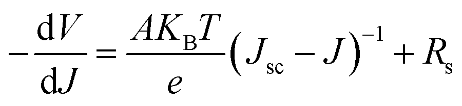
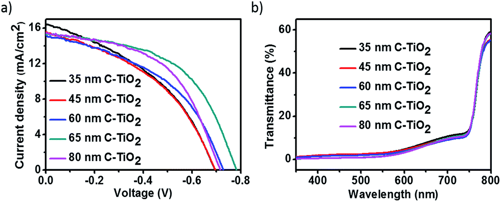
To investigate the FTO/perovskite contact, TiO2 compact (C-TiO2) and TiO2 mesoporous (M-TiO2) layers with different thickness were prepared on FTO substrates. C-TiO2 layers were spin-coated on FTO at varing speeds. The sectional SEM images of C-TiO2 layers with different thickness were shown in Fig. S1,† showing that the thickness of C-TiO2 layer increased from about 35 nm, 45 nm, 60 nm, 65 nm to 80 nm with the speed decreasing from 8000, 7000, 6000, 5000 to 4000 rpm. Perovskite materials and graphite electrode were then prepared on the C-TiO2 layers to assemble the photovoltaic devices. Afterwards, the linear sweep voltammetry measurement of the devices were carried out. The J–V curves under illumination are presented in Fig. 2a and the corresponding photovoltaic parameters are shown in Table 1. The shunt resistance (Rsh) and series resistance (Rs) were calculated from J–V curves as reported previously.38 The value of Rs could be determined by the following equation:
where V is the bias voltage applied to the device, J is the current density, A is the diode ideality factor, KB is the Boltzmann constant, T is temperature, and e is the elementary charge. Rs can be obtained from a linear fitting of −dV/dJ vs. (Jsc − J)−1. The value of Rsh could be determined by the following equation:
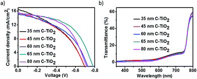 |
| | Fig. 2 (a) J–V curves and (b) transmittance curves of perovskites on various thickness C-TiO2 under illumination. | |
Table 1 Photovoltaic parameters of the perovskite solar cells with various thickness C-TiO2 layers
| C-TiO2 |
Jsc (mA cm−2) |
Voc (V) |
FF |
η (%) |
Rs (Ω cm2) |
Rsh (Ω cm2) |
| 35 nm |
16.4 |
0.695 |
0.41 |
4.6 |
4.6 |
114 |
| 45 nm |
15.6 |
0.695 |
0.42 |
4.6 |
5.4 |
114 |
| 60 nm |
15.2 |
0.729 |
0.45 |
5.0 |
8.3 |
186 |
| 65 nm |
15.3 |
0.784 |
0.53 |
6.3 |
10.4 |
296 |
| 80 nm |
15.4 |
0.717 |
0.53 |
5.8 |
10.5 |
279 |
The equation is applicable when V is near 0. The Voc of these devices increased from 0.695 V to 0.784 V as C-TiO2 layer thickness increased from 35 nm to 65 nm, and the shunt resistances improved from 114 Ω cm2 to 296 Ω cm2. The Jsc of these devices didn't greatly change, which may attributed to the similar light transmittance characters as shown in Fig. 1b. The results indicate a reduction of FTO/perovskite contact area with thicker C-TiO2 layers. When the thickness of C-TiO2 layer further increased to 80 nm, there were some visible particles in the film, which resulted in a lower performance of the device. The device with 60 nm thick C-TiO2 layer showed the best performance with the photoelectrical efficiency of 6.3%, Jsc of 15.3 mA cm−2, Voc of 0.784 V and FF of 0.53. In order to further decrease FTO/perovskite contact, M-TiO2 layers with different thickness were coated onto 60 nm C-TiO2 layer.
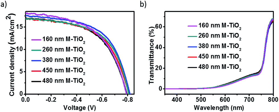
M-TiO2 layers were also prepared by spin-coating with different speed. Fig. S2† presents the cross-sectional SEM images of M-TiO2 layers, with thickness varing from 160 nm, 260 nm, 380 nm, 450 nm to 480 nm. Different photovoltaic devices were then fabricated using M-TiO2 layers of various thickness. J–V curves under illumination and detail parameters of the devices are recorded in Fig. 3a and Table 2, respectively. It can be seen that the performance improved greatly after the introduction of M-TiO2 layers. Compared with devices on C-TiO2 layer, the Voc of devices on M-TiO2/C-TiO2 improved from 0.695–0.784 V to 0.790–0.817 V, and the shunt resistance increased from 114–296 Ω cm2 to 340–577 Ω cm2. The enhanced performances suggested that FTO/perovskite contact area was further decreased by adding a TiO2 mesoporous layer. The Jsc of devices with M-TiO2 showed a slight decrease with M-TiO2 thickness increasing though they showed similar absorption (Fig. 3b), which may result from the increasing series resistances. The most efficient device showed an efficiency of 8.2% with Jsc of 17.5 mA cm−2, Voc of 0.817 V, FF of 0.57 with a 380 nm thick M-TiO2 layer.
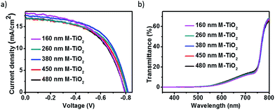 |
| | Fig. 3 (a) J–V curves and (b) transmittance curves of perovskites on various thickness M-TiO2 under illumination. | |
Table 2 Photovoltaic parameters of the perovskite solar cells with various thickness M-TiO2 layers
| M-TiO2 |
Jsc (mA cm−2) |
Voc (V) |
FF |
η (%) |
Rs (Ω cm2) |
Rsh (Ω cm2) |
| 160 nm |
18.2 |
0.790 |
0.53 |
7.6 |
10.7 |
340 |
| 260 nm |
17.0 |
0.794 |
0.55 |
7.4 |
12.7 |
432 |
| 380 nm |
17.5 |
0.817 |
0.57 |
8.2 |
12.1 |
410 |
| 450 nm |
16.8 |
0.808 |
0.58 |
7.8 |
16.4 |
577 |
| 480 nm |
16.7 |
0.810 |
0.56 |
7.6 |
13.4 |
454 |
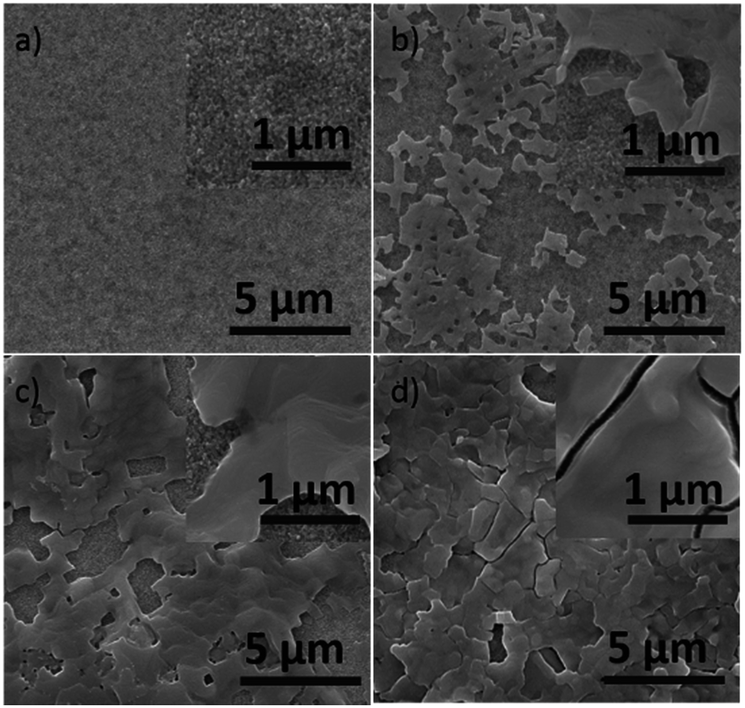
Another unfavorable carrier recombination process might happen in TiO2/graphite contact in the case that perovskite layer was not compact enough. In order to investigate the influence of the TiO2/graphite contact on device performance, different-coverage perovskites were spin-coated on M-TiO2 layers. By controlling the concentration of precursor solution, different coverage of perovskite were prepared. The typical top-view SEM images of them were shown in Fig. 4. These results suggested that the coverage become higher with the solution concentration increasing. X-ray diffraction (XRD) experiment was carried out to examine the crystal structure of the perovskite material. Fig. S3† showed the three-dimensional schematic representation and the corresponding XRD pattern. The materials presented a tetragonal perovskite structure with lattice parameters a = 8.825 Å, b = 8.835 Å, c = 11.24 Å. The intense diffraction peaks appeared at 14.20°, 28.58°, and 43.27°, which could be respectively assigned to (110), (220), (330) diffractions of the tetragonal phase.
 |
| | Fig. 4 Typical SEM images of perovskite morphologies on TiO2 surface with different coverages. | |
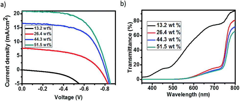
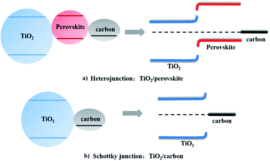
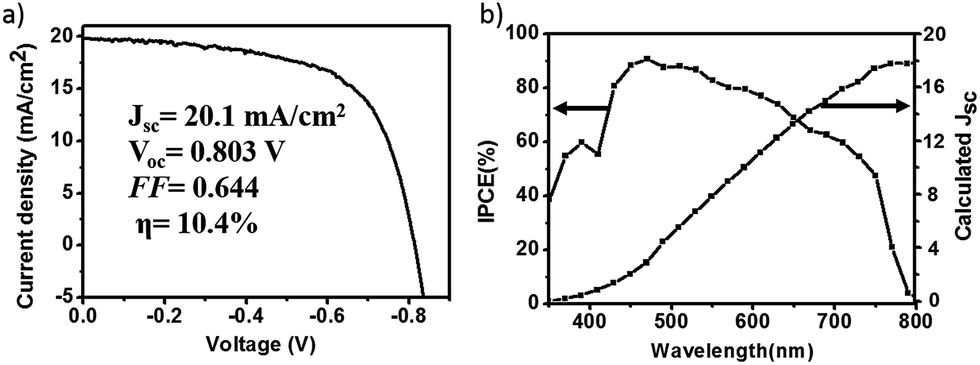
The J–V curves under illumination and light transmittance spectra of devices with different coverage perovskite were recorded in Fig. 5, and the detail parameters are presented in Table 3. It can be seen from Fig. 5a that the performance of devices improved a lot with the increase of perovskite coverage. The efficiency of devices increased from almost zero to 2.8% as the concentration of precursor solution increased from 13.2% to 26.4%, which resulted from both the increase of light absorption (Fig. 5b) and the improvement of perovskite coverage (Fig. 4). As the concentration of precursor solution further increased, the coverage of perovskite continued to increase, resulting in the improvement of device performances. Since perovskite film was not compact, the uncovered TiO2 came into contact with the graphite electrode. A Schottky junction was formed when TiO2 came into contact with graphite electrodes. We here saw a parallel with the TiO2/perovskite heterojunction as shown in Fig. 6. To study the effect of TiO2/graphite contact, a device with graphite electrode printing on pure TiO2 was fabricated. The resulting J–V curves are shown in Fig. S4.† It can be seen that the J–V curve recorded in the dark showed good rectifying performance whereas the J–V curve recorded in the light was almost a straight line, indicating the TiO2/graphite contact acted as an ohmic contact. This might be due to the increasing surface state densities of TiO2 induced by UV-light,39 which made a smaller contact potential difference between TiO2 and graphite. For these reasons, the TiO2/graphite contact was more like an ohmic contact. The parallel resistances of the devices under illumination were calculated as shown in Table 3. They increased from 329 Ω cm2 to 2287 Ω cm2 with the perovskite coverage increasing, leading to larger photo-voltages and better performances of the devices. In optimal conditions, a device showed an efficiency of 10.4% with Jsc of 20.1 mA cm−2, Voc of 0.803 V, FF of 0.644 as presented in Fig. 7a. The monochromatic incident photon-to-electron conversion efficiency (IPCE) data was illustrated in Fig. 7b with the highest value up to 90% at 470 nm. That being said, there are still great potential to improve the device performance, especially the photo-voltage.
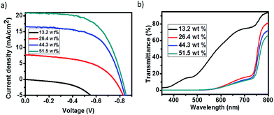 |
| | Fig. 5 (a) J–V curves and (b) transmittance curves of perovskites with different coverages under illumination. | |
Table 3 Photovoltaic parameters of perovskite solar cells with different-coverage perovskites
| Precursor concentration |
Jsc (mA cm−2) |
Voc (V) |
FF |
η (%) |
Rsh (Ω cm2) |
| 13.2% |
0.006 |
0.002 |
0.28 |
3.4 × 10⁻⁶ |
329 |
| 26.4% |
7.7 |
0.750 |
0.48 |
2.8 |
500 |
| 44.3% |
16.6 |
0.804 |
0.60 |
8.0 |
574 |
| 51.5% |
20.1 |
0.820 |
0.60 |
10.3 |
2287 |
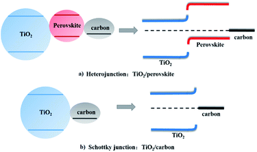 |
| | Fig. 6 Energy band diagrams of (a) TiO2/perovskite heterojunction and (b) TiO2/carbon Schottky junction. | |
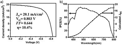 |
| | Fig. 7 (a) J–V curves of a best performed device and (b) the corresponding IPCE of the device. | |
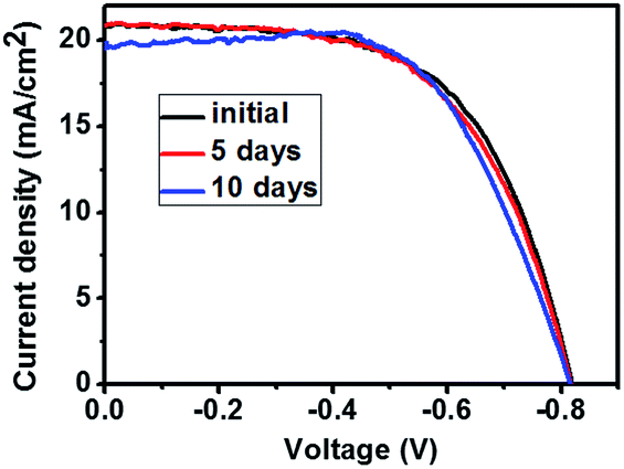
The stability of the device was further tested. The stabilized-power output curve under illumination of the device was measured in Fig. S6,† showing a steady efficiency of 9.2% over 400 s. A device was left in ambient atmosphere for 10 days to measure its stability. The J–V curves and photovoltaic parameters were shown in Fig. 8 and Table 4. The device efficiency dropped to 10.2% after 10 days, which was comparable with the initial efficiency of 10.3%. Furthermore, we immersed an unsealed device in water for 1 minute and tested its performance before and after immersion. Photos of device before and after immersion were shown in Fig. S7.† It can be seen that the perovskite without graphite turned to be yellow, while the one with graphite kept being black. Though the efficiency lowered from the initial 9.72% to 8.31%, it increased to 8.93% after 1 day by just leaving it in ambient atmosphere (Fig. S8, Table S3†).
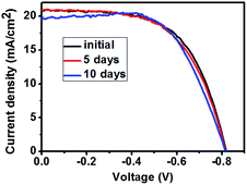 |
| | Fig. 8 Stabilities of a perovskite solar cell under ambient atmosphere. | |
Table 4 Photovoltaic parameters of a perovskite solar cells in ambient atmosphere for different days
| Days |
Jsc (mA cm−2) |
Voc (V) |
FF |
η (%) |
| 0 |
20.8 |
0.820 |
0.60 |
10.3 |
| 5 |
20.6 |
0.817 |
0.60 |
10.1 |
| 10 |
19.4 |
0.821 |
0.64 |
10.2 |
Conclusions
In conclusion, HTM free perovskite solar cells with low temperature processed graphite electrodes were fabricated and two contact effects on device performances were investigated. It was found that both FTO/Perovskite and TiO2/graphite contact could degrade the device performance especially the photo-voltage, which could mainly be due to the carrier recombination process introduced by the contacts. By introducing a 65 nm C-TiO2 layer and 380 nm M-TiO2 layer, the FTO/perovskite contact was efficiently lowered down, leading an enhancement of the photo-voltage from 0.695 V to 0.817 V. The TiO2/graphite contact was decreased by improving the perovskite coverage on TiO2 surface, which helped the photo-voltage increase from almost zero to 0.820 V. Finally, a best efficiency of 10.4% was obtained. Stability experiments suggested that the devices had excellent stability, which stayed stable in ambient atmosphere for over 10 days. These results indicate that FTO/perovskite and TiO2/graphite contacts have important influence on improving the performances of HTM free perovskite solar cells with graphite electrodes, which is fundamental to further enhancing the device's performances.
Acknowledgements
This work was supported by the Ministry of Science and Technology (Grants 2011CB933002 and 2012CB932702) and National Science Foundation of China (Grants 61306079 and 61671022), and Beijing Municipal Science and Technology Commission (Grants Z171100002017003).
Notes and references
- A. Kojima, K. Teshima, Y. Shirai and T. Miyasaka, J. Am. Chem. Soc., 2009, 131, 6050 CrossRef CAS PubMed.
- W. S. Yang, J. H. Noh, N. J. Jeon, Y. C. Kim, S. Ryu, J. Seo and S. I. Seok, Science, 2015, 348, 1234 CrossRef CAS PubMed.
- H. S. Kim, C. R. Lee, J. H. Im, K. B. Lee, T. Moehl, A. Marchioro, S. J. Moon, R. H. Baker, J. H. Yum and J. E. Moser, Sci. Rep., 2012, 2, 591 Search PubMed.
- J. Burschka, N. Pellet, S. J. Moon, R. H. Baker, P. Gao, M. K. Nazeeruddin and M. Gratzel, Nature, 2013, 499, 316 CrossRef CAS PubMed.
- D. Bi, G. Boschloo, S. Schwarzmueller, L. Yang, E. M. J. Johansson and A. Hagfeldt, Nanoscale, 2013, 5, 11686 RSC.
- Y. Zhong, R. Munir, A. H. Balawi, A. D. Sheikh, L. Yu, M.-C. Tang, H. Hu, F. Laquai and A. Amassian, ACS Energy Lett., 2016, 1, 1049 CrossRef CAS.
- M. Liu, M. B. Johnston and H. J. Snaith, Nature, 2013, 501, 395 CrossRef CAS PubMed.
- H. Zhou, Q. Chen, G. Li, S. Luo, T. B. Song, H. S. Duan, Z. Hong, J. You, Y. Liu and Y. Yang, Science, 2014, 345, 542 CrossRef CAS PubMed.
- D. P. McMeekin, G. Sadoughi, W. Rehman, G. E. Eperon, M. Saliba, M. T. Horantner, A. Haghighirad, N. Sakai, L. Korte, B. Rech, M. B. Johnston, L. M. Herz and H. J. Snaith, Science, 2016, 351, 151 CrossRef CAS PubMed.
- J. H. Heo, S. H. Im, J. H. Noh, T. N. Mandal, C. S. Lim, J. A. Chang, Y. H. Lee, H. J. Kim, A. Sarkar, M. K. Nazeeruddin, M. Grätzel and S. I. Seok, Nat. Photonics, 2013, 7, 486 CrossRef CAS.
- D. Q. Bi, L. Yang, G. Boschloo, A. Hagfeldt and E. M. Johansson, J. Phys. Chem. Lett., 2013, 4, 1532 CrossRef CAS PubMed.
- S. D. Chavhan, O. Miguel, H. J. Grande, V. G. Pedro, R. S. Sánchez, E. M. Barea, I. M. Seró and T. Z. Ramon, J. Mater. Chem. A, 2014, 2, 12754 CAS.
- J. A. Christians, R. C. Fung and P. V. Kamat, J. Am. Chem. Soc., 2013, 136, 758 CrossRef PubMed.
- J. Li, J. X. Yao, H. R. Xia, W. T. Sun, J. Liu and L. M. Peng, Appl. Phys. Lett., 2015, 107, 1 Search PubMed.
- T. Gatti, S. Casaluci, M. Prato, M. Salerno, F. Di Stasio, A. Ansaldo, E. Menna, A. Di Carlo and F. Bonaccorso, Adv. Funct. Mater., 2016, 26, 7443 CrossRef CAS.
- A. L. Palma, L. Cinà, S. Pescetelli, A. Agresti, M. Raggio, R. Paolesse, F. Bonaccorso and A. Di Carlo, Nano Energy, 2016, 22, 349 CrossRef CAS.
- M. Lee, Y. Ko, B. K. Min and Y. Jun, ChemSusChem, 2016, 9, 31 CrossRef CAS PubMed.
- J. Troughton, D. Bryant, K. Wojciechowski, M. J. Carnie, H. Snaith, D. A. Worsley and T. M. Watson, J. Mater. Chem. A, 2015, 3, 9141 CAS.
- J. Deng, L. Qiu, X. Lu, Z. Yang, G. Guan, Z. Zhang and H. Peng, J. Mater. Chem. A, 2015, 3, 21070 CAS.
- L. Etgar, P. Gao, Z. Xue, Q. Peng, A. K. Chandiran, B. Liu, M. K. Nazeeruddin and M. Graetzel, J. Am. Chem. Soc., 2012, 134, 17396 CrossRef CAS PubMed.
- W. A. Laban and L. Etgar, Energy Environ. Sci., 2013, 6, 3249 CAS.
- S. Aharon, B. E. Cohen and L. Etgar, J. Phys. Chem. C, 2014, 118, 17160 CAS.
- D. Bi, A. M. El-Zohry, A. Hagfeldt and G. Boschloo, ACS Appl. Mater. Interfaces, 2014, 6, 18751 CAS.
- Z. Liu, T. Shi, Z. Tang, B. Sun and G. Liao, Nanoscale, 2016, 8, 7017 RSC.
- H. Chen, X. Zheng, Q. Li, Y. Yang, S. Xiao, C. Hu, Y. Bai, T. Zhang, K. S. Wong and S. Yang, J. Mater. Chem. A, 2016, 4, 12897 CAS.
- Z. Liu, B. Sun, T. Shi, Z. Tang and G. Liao, J. Mater. Chem. A, 2016, 4, 10700 CAS.
- F. Zhang, X. Yang, M. Cheng, W. Wang and L. Sun, Nano Energy, 2016, 20, 108 CrossRef CAS.
- Z. Ku, Y. Rong, M. Xu, T. Liu and H. Han, Sci. Rep., 2013, 3, 3132 Search PubMed.
- A. Mei, X. Li, L. Liu, Z. Ku, T. Liu, Y. Rong, M. Xu, M. Hu, J. Chen, Y. Yang, M. Gratzel and H. Han, Science, 2014, 345, 295 CrossRef CAS PubMed.
- Y. Rong, Z. Ku, A. Mei, T. Liu, M. Xu, S. Ko, X. Li and H. Han, J. Phys. Chem. Lett., 2014, 5, 2160 CrossRef CAS PubMed.
- L. Liu, A. Mei, T. Liu, P. Jiang, Y. Sheng, L. Zhang and H. Han, J. Am. Chem. Soc., 2015, 137, 1790 CrossRef CAS PubMed.
- C. Y. Chan, Y. Wang, G.-W. Wu and E. Wei-Guang Diau, J. Mater. Chem. A, 2016, 4, 3872 CAS.
- K. Cao, Z. Zuo, J. Cui, Y. Shen, T. Moehl, S. M. Zakeeruddin, M. Grätzel and M. Wang, Nano Energy, 2015, 17, 171 CrossRef CAS.
- H. Li, K. Cao, J. Cui, S. Liu, X. Qiao, Y. Shen and M. Wang, Nanoscale, 2016, 8, 6379 RSC.
- H. Zhou, Y. Shi, Q. Dong, H. Zhang, Y. Xing, K. Wang, Y. Du and T. Ma, J. Phys. Chem. Lett., 2014, 5, 3241 CrossRef CAS PubMed.
- Y. Yang, J. Xiao, H. Wei, L. Zhu, D. Li, Y. Luo, H. Wu and Q. Meng, RSC Adv., 2014, 4, 52825 RSC.
- H. Wei, J. Xiao, Y. Yang, S. Lv, J. Shi, X. Xu, J. Dong, Y. Luo, D. Li and Q. Meng, Carbon, 2015, 93, 861 CrossRef CAS.
- J. Shi, J. Dong, S. Lv, Y. Xu, L. Zhu, J. Xiao, X. Xu, H. Wu, D. Li, Y. Luo and Q. Meng, Appl. Phys. Lett., 2014, 104, 063901 CrossRef.
- T. Leijtens, G. E. Eperon, S. Pathak, A. Abate, M. M. Lee and H. J. Snaith, Nat. Commun., 2013, 4, 2885 Search PubMed.
Footnote |
| † Electronic supplementary information (ESI) available: Fig. S1–S9: cross-sectional SEM images of TiO2 compact and mesoporous layers, schematic structure of perovskite materials and the corresponding XRD pattern, J–V curves of a device with carbon on pure TiO2, hysteresis effects, photo-stability of the PSCs, photographs and corresponding photovoltaic parameters of PSCs by water-corrosion. See DOI: 10.1039/c7ra00066a |
|
| This journal is © The Royal Society of Chemistry 2017 |
Click here to see how this site uses Cookies. View our privacy policy here. 
 Open Access Article
 This Open Access Article is licensed under a Creative Commons Attribution-Non Commercial 3.0 Unported Licence
 ab,
W. T. Sun
ab,
W. T. Sun