
 Open Access Article
 This Open Access Article is licensed under a
 Creative Commons Attribution 3.0 Unported Licence
Fabrication of arrayed triangular micro-cavities for SERS substrates using the force modulated indention process
Yongda Yan *ab,
Jingran Zhangab,
Ping Xuc and
Peng Miaoc
*ab,
Jingran Zhangab,
Ping Xuc and
Peng Miaoc
aThe State Key Laboratory of Robotics and Systems, Robotics Institute, Harbin Institute of Technology, Harbin 150080, P. R. China. E-mail: yanyongda@hit.edu.cn; Fax: +86-451-86415244; Tel: +86-451-86412924
bCenter for Precision Engineering, Harbin Institute of Technology, Harbin, Heilongjiang 150001, P. R. China
cSchool of Chemistry and Chemical Engineering, Harbin Institute of Technology, Harbin, Heilongjiang 150001, P. R. China
First published on 17th February 2017
Abstract
Based on the tip-based continuous indentation process, a novel method for the fabrication of periodic arrayed triangular micro-cavities on copper (Cu) surfaces is presented. The indentation force is modulated and the indentation speed and moving velocity of the precision stage used to drive the workpiece are optimized to improve the machining efficiency. The deformation property of the pile-ups at the side of the pyramidal cavity is studied. Due to the overlap of the pile-ups of adjacent micro pyramidal cavities, two and three dimensional arrayed nanostructures are successfully achieved. Then, the structured Cu (110) surface is used as a surface-enhanced Raman scattering (SERS) substrate with the rhodamine 6G (R6G) probe molecule as the detecting target in the present study. Experimental results show that the Raman intensity is enhanced with a decrease in the moving velocity of the precision stage. SERS enhancement factors within the range of 105 to 3 × 10⁶ are achieved on the structured Cu (110) surface, which demonstrates that this method is reliable, replicable, homogeneous and inexpensive for the fabrication of SERS substrates.
1. Introduction
Micro and nano machining technology has become a important research topic and is attracting increasing research attention.1–3 Various micro/nanostructures, including micro/nanowells, micro/nanochannels, micro/nanodomes and even three dimensional microstructures, which play important roles in microchip cooling,4,5 solar cells,6,7 plasmonic-enhanced photovoltaics8–10 and surface-enhanced Raman scattering (SERS),11,12 have been successfully fabricated via the existing micro/nanomachining methods.Metal micro/nanostructures have been already verified for use as SERS substrates. Several years ago, researchers found that the rough surface of some noble metals (gold, silver and copper), nanoparticles or specific arrayed structures could enhance energy transfer between a metal substrate and molecules and avoid fluorescence background interference. Compared with traditional Raman spectroscopy, surface enhanced Raman spectroscopy provides improved detection sensitivity. Therefore, SERS applications have experienced a huge growth in the past decade and span a wide range of fields, including biosensing and bioanalysis,13,14 bacteria and virus identification,15,16 and the detection of explosives17,18 and toxic pesticides.19
Typically, micro/nanostructures are mainly machined by lithography-based technologies, including electron-beam lithography (EBL),20–22 colloidal lithography (CL),23,24 template-assisted lithography (TAL),25 nanoimprint lithography (NIL),26,27 soft interference lithography (SIL),28–30 nanosphere lithography (NSL)31,32 and laser interference lithography (LIL).33 In addition, micro/nanostructures are also machined by hybrid lithography methods combined with other methods, such as dry etching34–36 and wetting etching.37–41 For example, Ye et al.35 designed and fabricated Ag nanowell crystals by colloidal lithography and O2 plasma etching. The nanowells, which were 483 nm in width and 40 nm in depth, were used as a label-free biosensor. Klarite SERS substrates with the specific apex angle of 70.5° on the Si (100) plane were fabricated using optical lithography and wetting etching method.39–41 Nanohole and nanopyramid arrayed structures were fabricated by Odom29 using the nanofabrication techniques involved in soft interference lithography (PDMS photomask), lift-off, electron-beam deposition and wetting etching. Different shapes of micro/nanostructures with a wide range can be machined by lithography-based methods. However, the major limitations of these methods are the sophistication (complexity) of the fabrication processes, inevitable defects and high cost.
Recently, the nanoindentation method was employed for the fabrication of micro/nanostructures with ordered shapes and ordered dimension structures. Gong et al.42 machined micro/nanostructures on silica film and epoxy substrates, including split rings, cavities and channels. SERS-active substrates were obtained using the transfer technique and the metal film deposition method. A self-assembled monolayer was formed on the pyramidal structures of the silver surface, and the enhancement factor of the Raman signal was 107 to 108 at the tip of the pyramidal structure. Chang et al.43–45 used this method to fabricate arrayed nanocavities with a controllable indentation depth and tip-to-tip displacements on the Au surface. In addition, EMCV, adenovirus and influenza virus were detected and DNA hybridization was analyzed using the nanocavities as SERS substrates. In their studies, they used a commercial nanoindenter, which is widely used to detect the mechanical properties of hardness, elastic modulus and friction coefficient. However, the commercial nanoindentation system has the shortcomings of small machining scale, low machining speed and high cost. In addition, it is difficult to obtain more complex micro/nanostructures with a wide range using this system.
Therefore, in the present study, a novel tip-based force modulated indention method is employed to fabricate arrayed triangular micro-cavities. By controlling the period of the force signal and the machining velocity of the precision stage, the property of the formed pile-ups on the Cu (110) plane is studied and different arrayed micro/nano-cavities based structures are formed by the overlap of the pile-ups. Finally, the Raman intensities of R6G are detected on the arrayed structures, which are used as SERS substrates.
2. Experimental
2.1 The principle of the force modulated indention process
Fig. 1 shows a schematic of the home-built tip-based force modulated indentation system and the machining process for the fabrication of substrates with periodic micro/nano-cavities. As shown in Fig. 1(a), the x–y precision stage (P-517, PI, Germany) with the movement range of 100 μm is used to drive the sample to control the x–y scale of the periodic micro/nano-cavities array, as shown in Fig. 1(b) and (c). The z axis precision stage with the range of 30 μm is used to make the diamond tip with the tip radius of less than 200 nm (Synton-MDP, Switzerland) to penetrate the sample surface according to the normal force signal, as shown in Fig. 1(b). The strain gauge force sensor with a 50 g capacity (LSB-200, Futek, USA) is employed to measure the normal force signal and keeps the diamond tip contacting the sample with the required force. The three stages are all driven by a UMAC controller (Delta Tau Data Systems, USA). The force signal is also captured by a port of the same UMAC. The single crystal copper (Cu (110)) of 10 mm × 5 mm × 1 mm is used as the sample (Heifei Ke Jing Materials Technology Co., LTD, China). Fig. 1(d) shows a scanning electron microscopy (Helios Nanolab 600i, Germany) image of the cube corner tip with its pyramidal shape.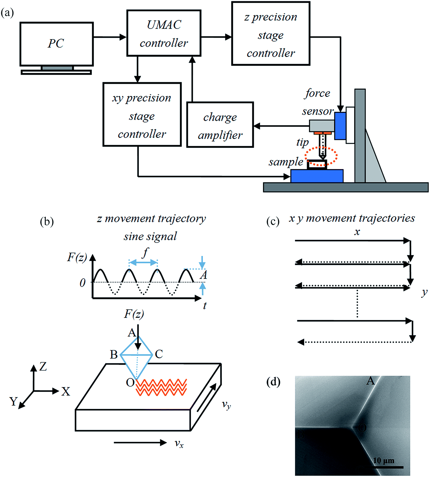 | ||
| Fig. 1 (a) Schematic of the home-built tip-based force modulated indentation system. (b) Machining process for the fabrication of substrates with periodic micro/nano-cavities. (c) Movement trajectories of the x and y directions during machining. (d) SEM image of the cube corner tip with its shape. | ||
Based on this system, the principle of fabricating periodic micro/nano cavities with the normal force modulation is presented as follows:
(1) The z axis precision stage brings the diamond tip to penetrate the sample surface to perform an indentation process. Only one cavity is obtained using this process, which is similar to the conventional indentation process.
(2) As shown in Fig. 1(b), a continuous sinusoidal signal of the normal force generated by the UMAC controller is used to move the z axis stage up and down to ensure the constant depth of each cavity in the present study. The depth of each cavity is determined by the amplitude (A) of the sinusoidal signal. Under this condition, the indentation process with a constant indentation depth is repeated.
(3) For procedure (2), if the x–y stage does not move the sample, the tip indents the same location repeatedly. If the x stage moves the sample with a velocity of vx simultaneously, as shown in Fig. 1(b), the continuous indentation processes will be separated. The distance between adjacent cavities is controlled by the period (f) of the sinusoidal signal and the moving velocity of the x stage (vx). Linear periodic micro/nano-cavities are generated with high efficiency using this method.
(4) The y stage controls the sample to move to the other position after one line structure is fabricated, as shown in Fig. 1(c). Then, cavity arrays can be obtained, as shown in Fig. 1(b). The length and width of the microstructure array are controlled by the moving scales of the x and y stage, respectively.
2.2 Measurement devices used in this study
To perform Raman measurements, the structured copper samples were dipped into an R6G aqueous solution with a concentration of 10−6 M for 30 min and then rinsed with ethanol to remove the excessive R6G molecules and dried with a continuous gentle nitrogen flow before Raman spectroscopy measurement. A micro-Raman spectroscopic system (Renishaw, inVia, UK) equipped with a 633 nm wavelength laser and focused with a 50× objective was employed. Approximately 6.4 mW laser power was used to excite the samples and the beam diameter was approximately 1 μm. The signal detector used a Renishaw CCD camera (1040 × 256) and the grating size was 1800 l mm−1. The exposure time was 1 s and the accumulation number was 1. The mapping images of the micro-Raman spectrum were scanned over a 20 μm × 20 μm area and the Raman mapping step size was controlled at 1 μm. Before the tests, a standard Si substrate was employed to rectify the Raman spectrum and no specific peaks were found. The Raman intensity of R6G was chosen at 1362 cm−1 in the experiment, which is the major peak intensity of R6G molecules.A Dimension Icon AFM system (Bruker, Germany) was used to observe the topographies of the machined microstructures with the scan size of 50 μm × 50 μm. The elastic constant of the silicon cantilever was 0.2 N m−1 and contact mode was used.
3. Results and discussion
3.1 Fabrication of arrayed cavities on the Cu (110) sample surface
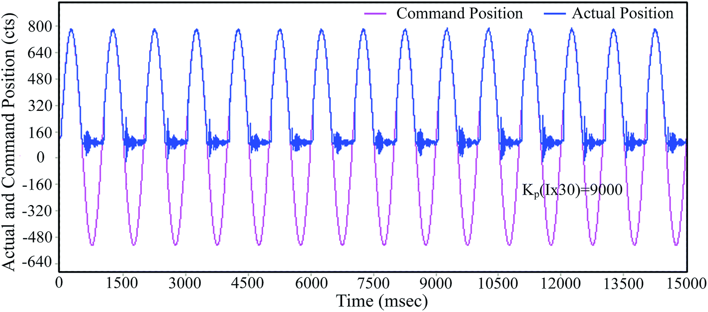 | ||
| Fig. 2 Force signals of the actual force (blue line) and the command force (pink line). | ||
The depth is an important parameter of the micro cavity. The relationship between the normal force and the machined depth must be known. In the present study, the depth of the micro cavity is predicted by the hardness formula, which is used in previous studies.46,47 The Berkovich hardness (H) can be expressed as a function of the applied normal force (Fn) and the projected area (A) of the cube corner tip after indentation, which is related to the penetration depth (H) in eqn (1). The face angle with respect to the central axis of the diamond tip (α), the penetration depth (h) and the projected area (A) are expressed as eqn (2), where, α is 35.26° for the cube corner tip, and the aluminum alloy hardness is 1.22 GPa, as measured using a Berkovich indenter. Therefore, the relationship between the normal force and the groove depth can be obtained from eqn (3) when using a cube corner tip. The groove depth is 1.79 μm with the normal force of 10 mN.
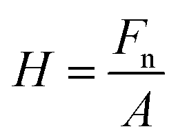 | (1) |
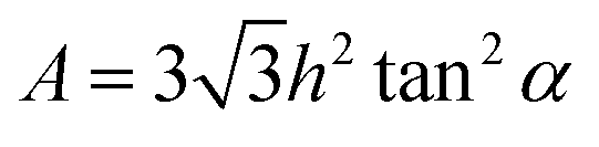 | (2) |
The penetration depth, h, can then be obtained from eqn (3) using eqn (1) and (2):
 | (3) |
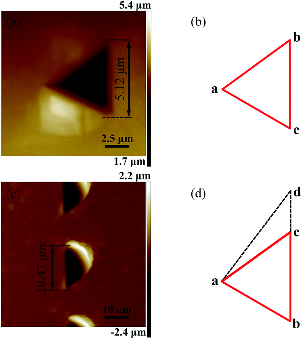 | ||
| Fig. 3 (a) AFM images of the inverted pyramid cavity when the precision stage is fixed. (b) Schematic shapes of the cavity when the precision stage is fixed. (c) AFM images of the inverted pyramid cavity when the precision stage is moved. (d) Schematic shapes of the cavity when the precision stage is moved. | ||
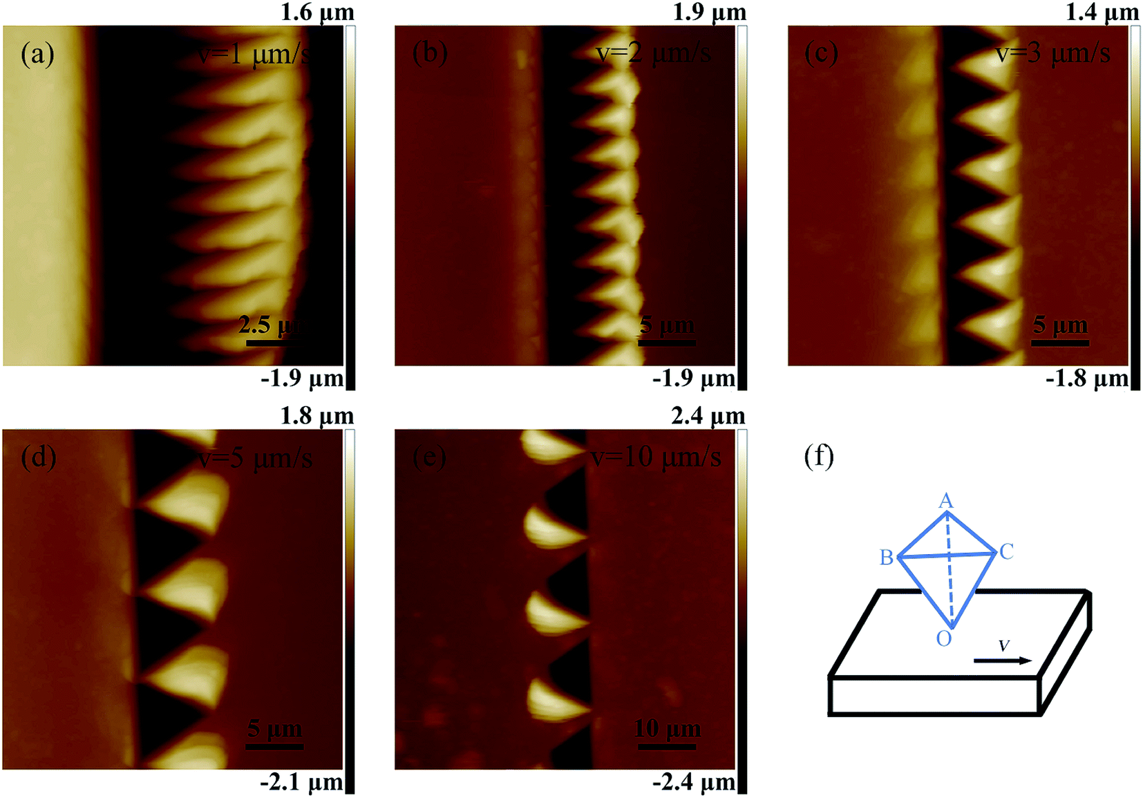 | ||
| Fig. 4 AFM images of the arrayed inverted pyramid cavities with different machining velocities with the plane AOC of the cube corner tip as the rake face (a)–(e) the machining velocity of 2, 3, 4, 5 and 10 μm s−1, respectively. (f) Schematic machining direction with the plane AOC of the cube corner tip. | ||
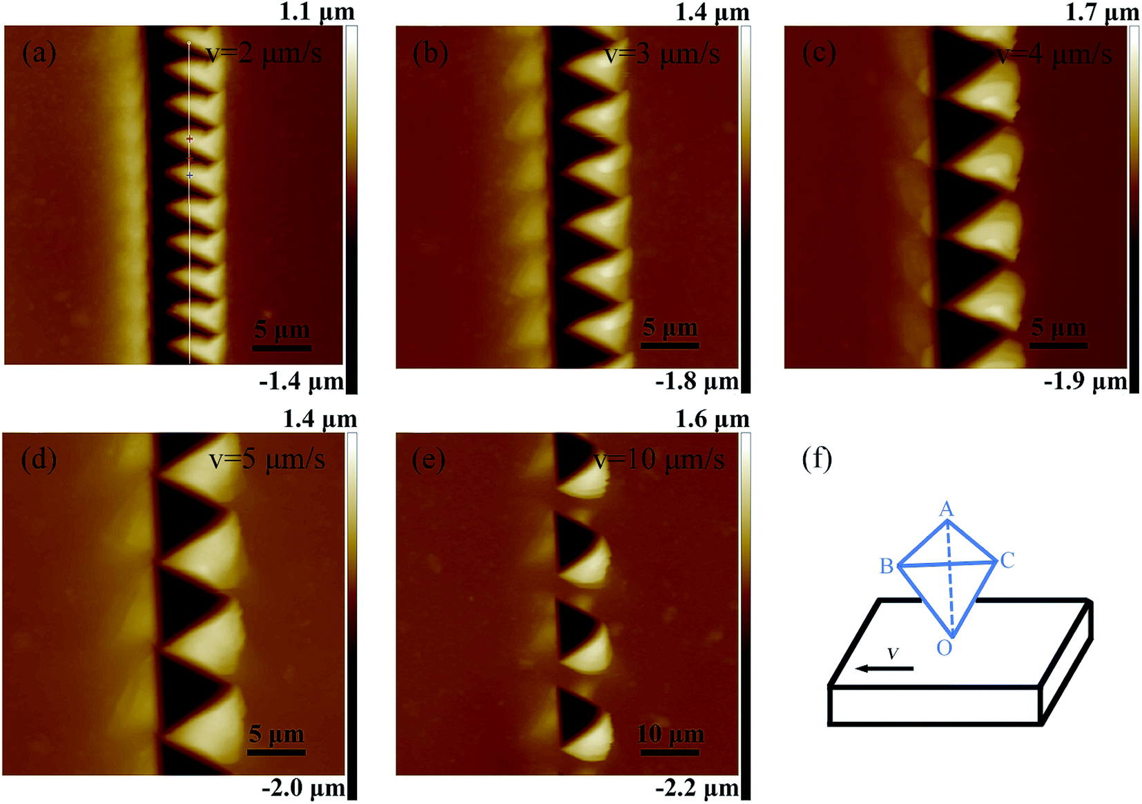 | ||
| Fig. 5 AFM images of arrayed inverted pyramid cavities with different machining velocities with the plane AOB of the cube corner tip as the rake face (a)–(e) the machining velocity of 2, 3, 4, 5 and 10 μm s−1, respectively. (f) Schematic machining direction with the plane AOC of the cube corner tip. | ||
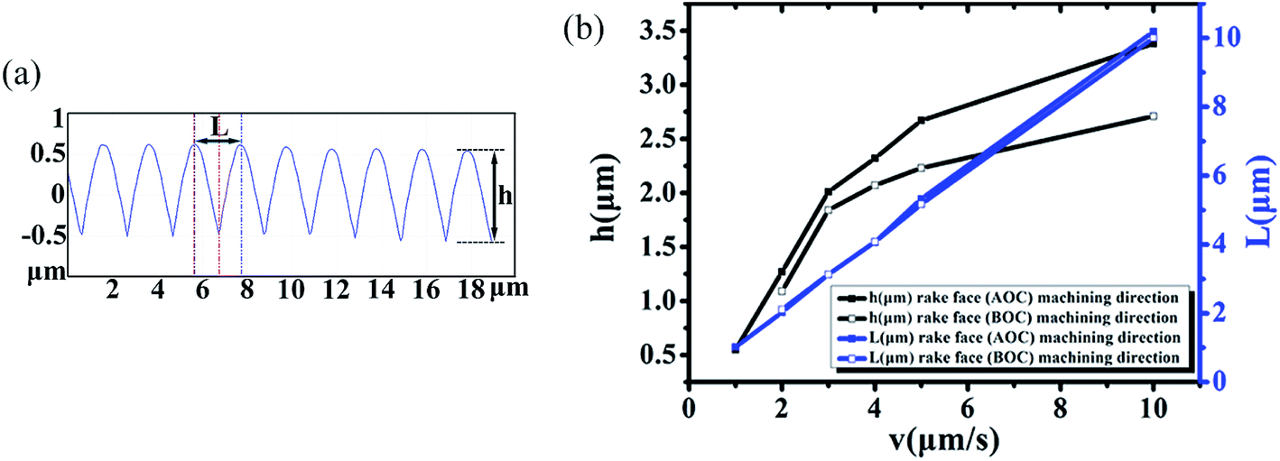 | ||
| Fig. 6 (a) Schematic diagram of the depth and the width of cavities. (b) Relationship between the dimensions of the cavities and the moving velocity of the precision stage. | ||
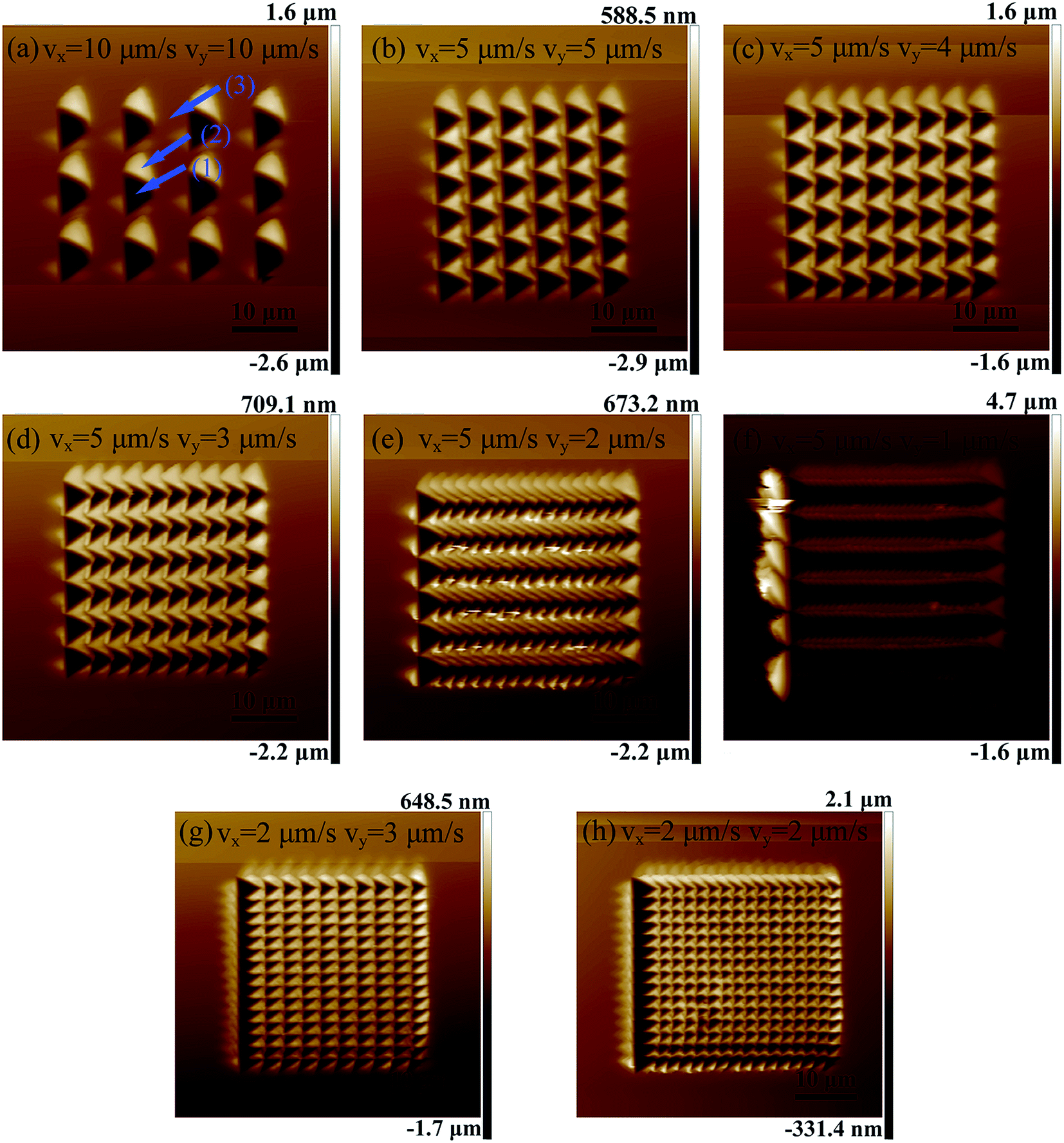 | ||
| Fig. 7 AFM images of the arrayed inverted pyramid cavities with different velocities (vx and vy). | ||
3.2 Raman enhancement of R6G molecules on the arrayed inverted pyramid cavities on Cu (110) substrates
In order to study the effect of Raman enhancement of R6G molecules with different arrayed inverted pyramid cavities, the parameters of the velocities of the x–y stage for machining arrayed micro/nano structures with a fixed normal force of 10 mN and 1 Hz using the method presented in this study are shown in Table 1. Fig. 8 shows the Raman intensity mapping images of absorbed R6G (1362 cm−1 peak) on the arrayed inverted pyramid cavities with three moving velocities of the stage in the x and y directions. The velocity (vx) ranges from 5 μm s−1 to 10 μm s−1 and the velocity (vy) ranges from 1 μm s−1 to 10 μm s−1. Raman spectra were collected with a step size of 1 μm along the x and y directions by a point mapping pattern. At each point, the spectra were collected for 1 s over two scans. The brighter the pixel, the higher the intensity. SERS spectra are observed in both the interior of the cavities and pile-ups formed near the cavities, as indicated by arrows (1) and (2) in Fig. 8(a), which correspond to the positions of arrows (1) and (2) in Fig. 7(a). However, there is no significant enhancement in the Cu (110) surface, as shown by arrow (3) in Fig. 8(a), which corresponds to the position of arrow (3) in Fig. 7(a). Essentially, the flat Cu surface, rather than the overlapped cavities, remained in this area with a larger moving velocity. The insets in Fig. 8(b) and (c) are AFM images corresponding to the field map. The correspondence between the topography of the “fish scale” profile and the near-field distribution mapping are clearly seen in Fig. 8(c). It is experimentally verified that the distributions of the Raman intensities are uniform along the same machining direction and it is demonstrated that this novel tip-based method has high reproducibility and reliability, as shown in Fig. 8(b) and (c).| (1) | (2) | (3) | (4) | (5) | (6) | (7) | (8) | (9) | (10) | (11) | (12) | (13) | (14) | |
|---|---|---|---|---|---|---|---|---|---|---|---|---|---|---|
| vx (μm s−1) | 10 | 5 | 5 | 5 | 5 | 5 | 4 | 4 | 4 | 4 | 2 | 2 | 2 | 2 |
| vy (μm s−1) | 10 | 5 | 4 | 3 | 2 | 1 | 4 | 3 | 2 | 1 | 4 | 3 | 2 | 1 |
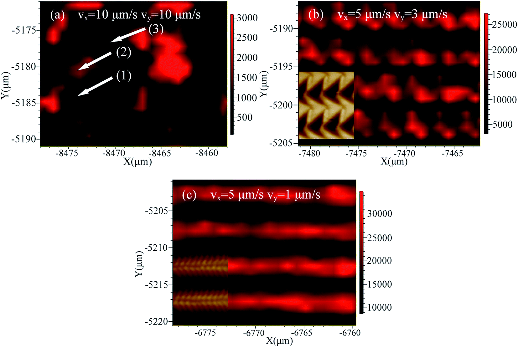 | ||
| Fig. 8 Raman intensity mapping images of the arrayed inverted pyramid cavities fabricated with three moving velocities of the stage (a) velocity of 10 μm s−1 in both x and y directions. (b) Velocity of 5 μm s−1 in the x direction and 3 μm s−1 in the y direction and the inset is the AFM image corresponding to the field map. (c) Velocity of 5 μm s−1 in the x direction and 1 μm s−1 in the y direction and the inset is an AFM image of the structure of the “fish scale” corresponding to the field map. | ||
The data of Raman mapping were exported to Raman spectra point by point. Prior to analysis, first, all the Raman spectra were smoothened using a Savitzky–Golay filter with a third-order polynomial and a smooth window size of 13. Second, the baseline of the Raman spectra was removed by subtracting a spline interpolation using WiRE 3.4.
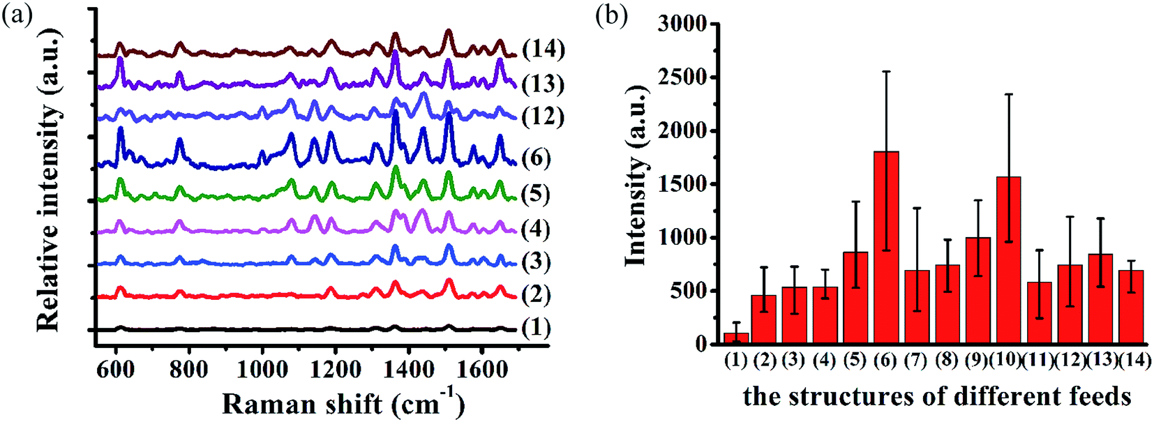
Fig. 9 shows the Raman spectra of R6G molecules on the structured Cu (110) substrate at a concentration of 10−6 M under different machining conditions. The characteristic peaks of the R6G molecules are shown at 612 cm−1, 771 cm−1, 1183 cm−1, 1311 cm−1, 1362 cm−1, 1504 cm−1 and 1603 cm−1. It can be observed that the Raman enhancement can be remarkably affected by the machining velocities in the x and y directions when the applied force has a constant variation rate.
 | ||
| Fig. 9 (a) Raman spectra of R6G molecules on the structured Cu (110) substrate at a concentration of 10−6 M with different machining velocities. (b) Average Raman intensity of the 1362 cm−1 R6G peak of 20 μm × 20 μm of arrayed inverted pyramid cavities with different machining velocities. | ||
All the characteristic peaks of the Raman intensity in curve (1) have a weaker enhancement in Fig. 9(a). This agrees well with the results shown in Fig. 8(a). Under this condition, the distance between the adjacent cavities is too large for them to be overlapped with each other, as shown in Fig. 7(a). The Raman intensity with the peak of 1362 cm−1 R6G increases with a decrease in velocity in the y direction, as shown by the curves (2)–(6) in Fig. 9(a). The Raman intensity with the velocity (vy) of 1 μm s−1 is the strongest.
Fig. 10(b)–(d) show an enlarged AFM image of the arrayed inverted pyramid cavities and three-dimensional and section views of the structures with the velocity (vx) of 5 μm s−1 and velocity (vy) of 1 μm s−1, respectively. The depths of the nanostructures are 116 nm, 233 nm and 260 nm in Fig. 10(d). In addition, the microstructures induced by the tip's trace are homogeneously distributed on the Cu (110) surface. The Raman intensity with the peak of 1362 cm−1 R6G does not significantly change and is weaker than that of the structures with the velocity (vx) of 5 μm s−1 and velocity (vy) of 1 μm s−1, as shown by the curves (12)–(14) in Fig. 9(a). Fig. 9(b) shows the average Raman intensity of the 1362 cm−1 R6G of 20 μm × 20 μm of the arrayed inverted pyramid cavities with different machining velocities, which correspond to Fig. 9(a). The structures of inverted cavities change on using different machining velocities. In addition, nanostructures obtained using different machining velocities are formed by the overlap and extrusion of the adjacent pyramid cavities. The depth of the nanostructures obtained using a velocity (vx) of 5 μm s−1 and velocity (vy) of 1 μm s−1 is shallower than the depths of the nanostructures obtained using other machining parameters.
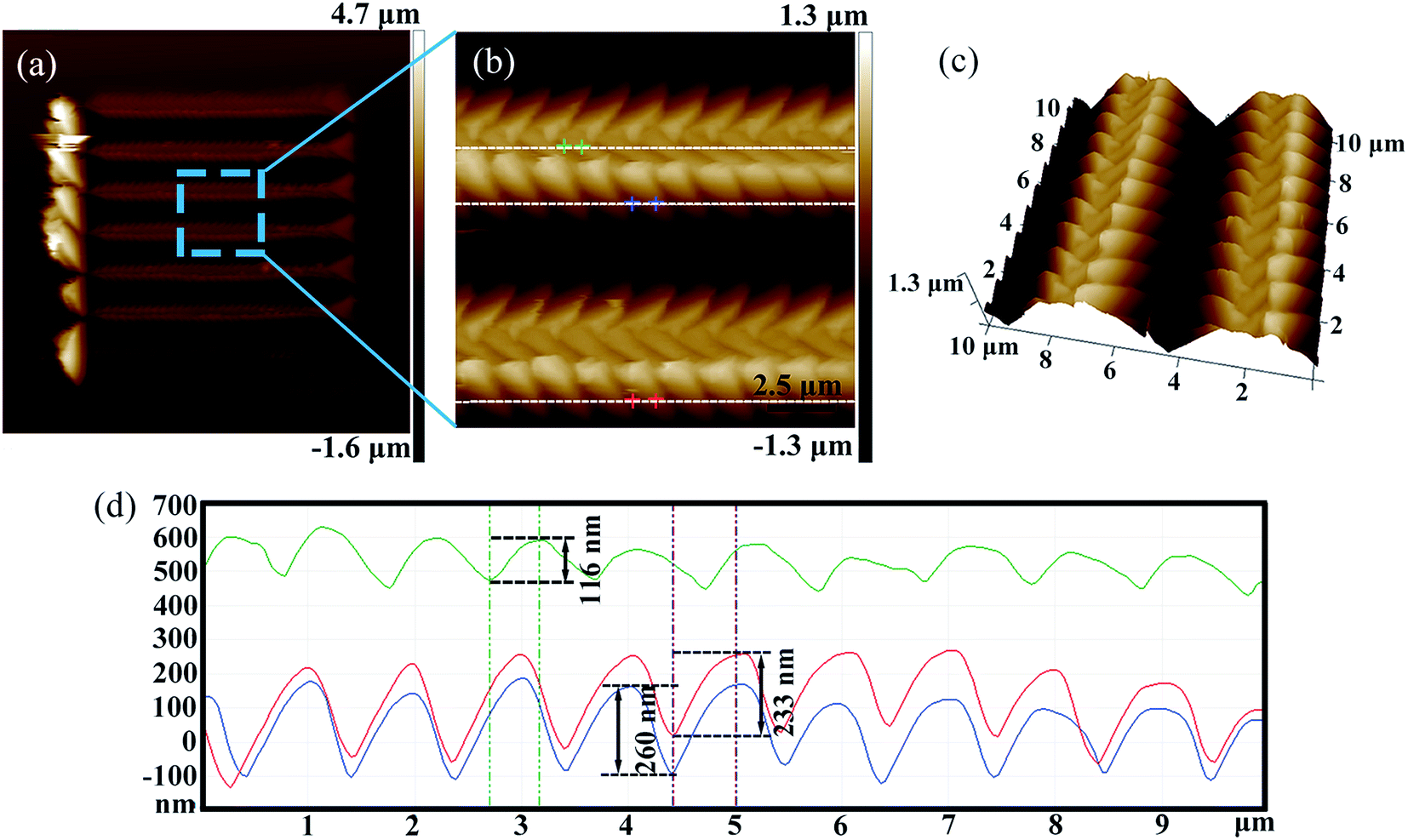 | ||
| Fig. 10 (a) AFM images of arrayed inverted pyramid cavities machined with vx = 5 μm s−1 and vy = 1 μm s−1. (b) Enlarged image of the local position of figure (a). (c) Three-dimensional view of structures with vx = 5 μm s−1 and vy = 1 μm s−1. (d) Sectional view of the structures in figure (b). | ||
Therefore, the average intensity of the velocity (vx) of 5 μm s−1 and velocity (vy) of 1 μm s−1 with the “fish scale” structure is the strongest, as shown in Fig. 9(b). When the velocity changes from 5 μm s−1 to 3 μm s−1, the intensity does not significantly change in Fig. 9(b). Previous studies obtained similar results. On one hand, more nanostructures are formed by different machining velocities, in particular the velocity of 5 μm s−1 in the x direction and 1 μm s−1 in the y direction, as shown in Fig. 7(f) and 10. Chang et al.43 showed that probe molecules are easily entrapped into the nanostructures and noticeably detected by the SERS effect. Therefore, it can be deduced that more R6G molecules can be adsorbed and entrapped by the nanostructures. On the other hand, with proper excitation of this absorption, a strong local electromagnetic field with the electromagnetic mechanism (EM) is generated with different structures. Compared with the bare surface, an electric field is generated and a plasmon may exist on the interior of the single V-groove, as shown by some researchers,48–50 forming very strong near fields and enhancing the Raman signal, which corresponds to Fig. 7(a). Furthermore, a much stronger Raman enhancement apparently occurs in the vicinity of the nanostructures, as shown in Fig. 7(b)–(h). Some researchers51,52 have demonstrated that the electric field intensity is influenced by the distance between adjacent pyramids. The “hot lines” formed by two adjacent nanostructures are formed by an infinite number of hot spots. Compared with the dispersed structures, the electric field intensity generated by adjacent structures is about 15 times that of the electric field intensity generated by dispersed structures.51 Therefore, compared with dispersed structures, the uniformity and stability of the electric field intensity from the molecules adsorbed on the numerous hot lines formed by the nanostructures are significantly enhanced, which agrees well with our experiment results.
The enhancement factors are calculated as follows:53,54
 | (4) |
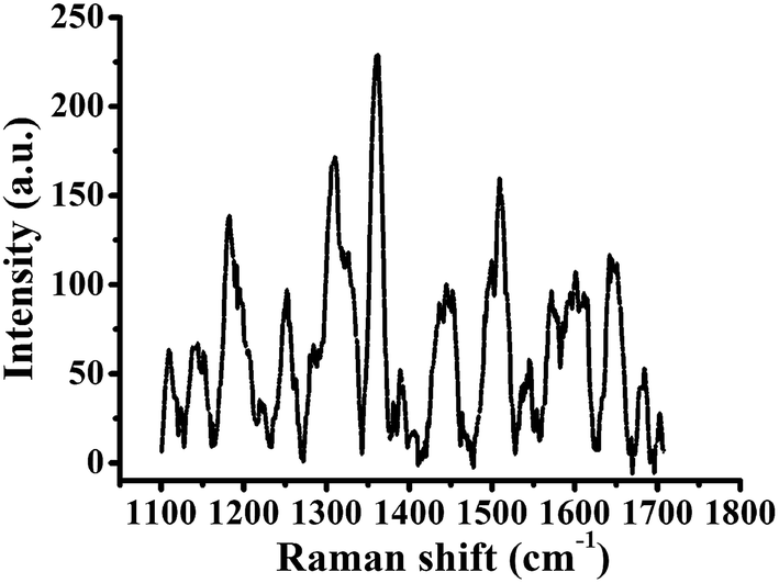 | ||
| Fig. 11 Raman spectra of R6G molecules on the SiO2 substrate at a concentration of 0.25 M. | ||
4. Conclusions
A novel method based on the tip-based force modulated nanoindentation process is employed to fabricate two and three dimensional arrayed micro/nano structures on the Cu (110) plane. By optimizing the x–y precision stage and z direction precision stage, complex arrayed micro cavities are achieved by detailed studies on the overlap of the pile-ups of adjacent micro cavities. Then, these arrayed micro structures can be used as structures for SERS substrates. The SERS intensity induced by these types of nanostructures machined using different machining parameters for R6G molecules is verified. The SERS enhancement factors are between 105 and 3 × 10⁶ for the structured single crystal copper (110) plane, which demonstrates that this method is reliable, replicable, homogeneous and inexpensive for machining large-area regular nanostructures. Therefore, this tip-based force modulated indentation method is expected to develop new opportunities for label-free SERS detection in biosensing and bioanalytics, bacteria and virus identification and the detection of explosives and toxic pesticides in the future.Acknowledgements
The authors gratefully acknowledge the financial supports of the Foundation for the National Natural Science Foundation of China (51675134), Innovative Research Groups of the National Natural Science Foundation of China (51521003), Self-Planned Task (SKLRS201606B) of State Key Laboratory of Robotics and System (HIT) and the National Program for Support of Top-notch Young Professors.References
- Z. L. Cao, S. L. Wong, S. Y. Wu, H. P. Ho and H. C. Ong, Appl. Phys. Lett., 2014, 104, 171116 CrossRef.
- P. P. Huang, Z. Z. Wang, L. Lin, Z. H. Feng, X. Wen and Z. Q. Zheng, Appl. Surf. Sci., 2016, 386, 345–351 CrossRef CAS.
- J. J. Zhang, J. G. Zhang, Z. F. Wang, A. Hartmaier, Y. D. Yan and T. Sun, Comput. Mater. Sci., 2017 DOI:10.1016/j.commatsci.2017.01.043.
- Y. J. Oh and K. H. Jeong, Lab Chip, 2014, 14, 865–868 RSC.
- A. Lee, G. H. Yeoh, V. Timchenko and J. A. Reizes, Appl. Therm. Eng., 2012, 48, 275–288 CrossRef.
- J. Liu, X. S. Zhang, C. Q. Dong, Y. X. Liao, B. Wang, T. C. Zhang and F. T. Yi, Appl. Surf. Sci., 2014, 289, 300–305 CrossRef CAS.
- J. Liu, M. Ashmkhan, G. Q. Dong, B. Wang and F. T. Yi, Sol. Energy Mater. Sol. Cells, 2013, 108, 93–97 CrossRef CAS.
- S. Lombardo, C. Tringali, G. Cannella, A. Battaglia, M. Foti, N. Costa, F. Principato and C. Gerardi, Appl. Phys. Lett., 2012, 101, 123902 CrossRef.
- C. A. Wolden, J. Kurtin, J. B. Baxter, I. Repins, S. E. Shaheen, J. T. Torvik, A. A. Rockett, V. M. Fthenakis and E. S. Aydil, J. Vac. Sci. Technol., A, 2011, 29, 030801 Search PubMed.
- W. Zhou, H. Gao and T. W. Odom, ACS Nano, 2010, 4, 1241–1247 CrossRef CAS PubMed.
- S. A. Kara, A. Keffous, A. M. Giovannozzi, A. M. Rossi, E. Cara, L. D'Ortenzi, K. Sparnacci, L. Boarino, N. Gabouze and S. Soukane, RSC Adv., 2016, 6, 93649–93659 RSC.
- S. Z. Oo, S. Siitonen, V. Kontturi, D. A. Eustace and M. D. B. Charlton, Opt. Express, 2016, 24, 724–731 CrossRef CAS PubMed.
- J. Y. Lin, A. D. Stuparu, M. D. Huntington, M. Mrksich and T. W. Odom, J. Phys. Chem. C, 2013, 117, 5286–5292 CAS.
- K. Nakamoto, R. Kurita, O. Niwa, T. Fujiicd and M. Nishida, Nanoscale, 2011, 3, 5067–5075 RSC.
- T. A. Alexander, Anal. Chem., 2008, 80, 2817–2825 CrossRef CAS PubMed.
- K. Karn-orachai, K. Sakamoto, R. Laocharoensuk, S. Bamrungsap, S. Songsivilai, T. Dharakul and K. Miki, RSC Adv., 2016, 6, 97791–97799 RSC.
- S. Botti, S. Almaviva, L. Cantarini, A. Palucci, A. Puiu and A. Rufoloni, J. Raman Spectrosc., 2013, 44, 463–468 CrossRef CAS.
- A. Hakonen, P. O. Andersson, M. S. Schmidt, T. Rindzevicius and M. Käll, Anal. Chim. Acta, 2015, 893, 1–13 CrossRef CAS PubMed.
- L. Wu, Z. Wang and B. Shen, Nanoscale, 2013, 5, 5274–5278 RSC.
- M. L. Jin, V. Pully, C. Otto, A. V. D. Berg and E. T. Carlen, J. Phys. Chem. C, 2010, 114, 21953–21959 CAS.
- A. Kinkhabwala, Z. F. Yu, S. H. Fan, Y. Avlasevich, K. Müllen and W. E. Moerner, Nat. Photonics, 2009, 3, 654–657 CrossRef CAS.
- J. Petschulat, D. Cialla, N. Janunts, C. Rockstuhl, U. Hübner, R. Möller, H. Schneidewind, R. Mattheis, J. Popp, A. Tünnermann, F. Lederer and T. Pertsch, Opt. Express, 2010, 18, 4184–4197 CAS.
- J. H. Zhang, Y. F. Li, X. M. Zhang and B. Yang, Adv. Mater., 2010, 22, 4249–4269 CrossRef CAS PubMed.
- J. Y. Park, Korean J. Chem. Eng., 2014, 31, 541–547 CrossRef CAS.
- Z. Tang and A. Wei, ACS Nano, 2012, 6, 998–1003 CrossRef CAS PubMed.
- H. Gao, C. Liu, H. E. Jeong and P. D. Yang, ACS Nano, 2011, 6, 234–240 CrossRef PubMed.
- K. Nakamoto, R. Kurita, O. Niwa, T. Fujii and M. Nishida, Nanoscale, 2011, 3, 5067–5075 RSC.
- H. Gao, J. C. Yang, J. Y. Lin, A. D. Stuparu, M. H. Lee, M. Mrksich and T. W. Odom, Nano Lett., 2010, 10, 2549–2554 CrossRef CAS PubMed.
- T. W. Odom, MRS Bull., 2010, 35, 66–73 CrossRef CAS.
- W. Zhou, H. Gao and T. W. Odom, ACS Nano, 2010, 4, 1241–1247 CrossRef CAS PubMed.
- Z. D. Zhu, Q. Q. Li, B. F. Bai and S. S. Fan, Nanoscale Res. Lett., 2014, 9, 1–8 CrossRef PubMed.
- T. J. Wang, K. C. Hsu, Y. C. Liu, C. H. Lai and H. P. Chiang, J. Opt., 2016, 18, 055006 CrossRef.
- M. Jin, H. V. Wolferen, H. Wormeester, A. V. D. Berga and E. T. Carlen, Nanoscale, 2012, 4, 4712–4718 RSC.
- Y. L. Ho, M. Abasaki and J. J. Delaunay, ACS Photonics, 2015, 2, 730–737 CrossRef CAS.
- S. S. Ye, X. M. Zhang, L. X. Chang, T. Q. Wang, Z. B. Li, J. H. Zhang and B. Yang, Adv. Opt. Mater., 2014, 2, 779–787 CrossRef CAS.
- H. Im, S. H. Lee, N. J. Wittenberg, T. W. Johnson, N. C. Lindquist, P. Nagpal, D. J. Norris and S. H. Oh, ACS Nano, 2011, 5, 6244–6253 CrossRef CAS PubMed.
- H. W. Gao, J. Henzie, M. H. Lee and T. W. Odom, Proc. Natl. Acad. Sci. U. S. A., 2008, 105, 20146–20151 CrossRef CAS PubMed.
- B. K. Chao, H. H. Cheng, L. W. Nien, M. J. Chen, T. Nagao, J. H. Li and C. H. Hsueh, Appl. Surf. Sci., 2015, 357, 615–621 CrossRef CAS.
- K. C. Vernon, T. J. Davis, F. H. Scholes, D. E. Gómez and D. Lau, J. Raman Spectrosc., 2010, 41, 1106–1111 CrossRef CAS.
- J. M. Li, X. X. Xu, Y. F. Wang, M. Wang, Z. F. Dong, W. H. Tian, J. M. Sun, C. Z. Zhang and B. Wang, J. Raman Spectrosc., 2012, 43, 863–868 CrossRef CAS.
- S. Botti, L. Cantarini, S. Almaviva, A. Puiub and A. Rufolonic, Chem. Phys. Lett., 2014, 592, 277–281 CrossRef CAS.
- J. L. Gong, D. J. Lipomi, J. D. Deng, Z. H. Nie, X. Chen, N. X. Randall, R. Nair and G. M. Whitesides, Nano Lett., 2010, 10, 2702–2708 CrossRef CAS PubMed.
- C. W. Chang, J. D. Liao, A. L. Shiau and C. K. Yao, Sens. Actuators, B, 2011, 156, 471–478 CrossRef CAS.
- C. K. Yao, J. D. Liao, C. W. Chang and J. R. Lin, Sens. Actuators, B, 2012, 174, 478–484 CrossRef CAS.
- C. K. Yao, J. D. Liao, C. H. Lin, Y. S. Yang, S. H. Yu and J. W. Yang, Sens. Actuators, B, 2014, 191, 219–226 CrossRef CAS.
- A. C. Fischer-Cripps and I. Mustafaev, Introduction to contact mechanics, Springer, New York, 2000 Search PubMed.
- J. M. Lee, W. H. Jin and D. E. Kim, Wear, 2001, 251, 1133–1143 CrossRef.
- K. C. Vernon, T. J. Davis, F. H. Scholes, D. E. Gómez and D. Lau, J. Raman Spectrosc., 2010, 41, 1106–1111 CrossRef CAS.
- C. L. C Smith, B. Desiatov, I. Goykmann, I. Fernandez-Cuesta, U. Levy and A. Kristensen, Opt. Express, 2012, 20, 5696–5706 CrossRef PubMed.
- F. H. Scholes, T. J. Davis, K. C. Vernon, D. Lau, S. A. Furman and A. M. Glenn, J. Raman Spectrosc., 2012, 43, 196–201 CrossRef CAS.
- R. Li, H. Li, S. Pan, K. Liu, S. S. Hu, L. J. Pan, Y. N. Guo and S. F. Wu, J. Mater. Res., 2013, 28, 3401–3407 CrossRef CAS.
- H. H. Cheng, S. W. Chen, Y. Y. Chang, J. Y. Chu, D. Z. Lin, Y. P. Chen and J. H. Li, Opt. Express, 2011, 19, 22125–22141 CrossRef CAS PubMed.
- Q. Shao, R. H. Que, M. W. Shao, L. Cheng and S. T. Lee, Adv. Funct. Mater., 2012, 22, 2067–2070 CrossRef CAS.
- W. B. Cai, B. Ren, X. Q. Li, C. X. She, F. M. Liu, X. W. Cai and Z. Q. Tian, Surf. Sci., 1998, 406, 9–22 CrossRef CAS.
| This journal is © The Royal Society of Chemistry 2017 |