
 Open Access Article
 This Open Access Article is licensed under a
 Creative Commons Attribution 3.0 Unported Licence
Films based on group IV–V–VI elements for the design of a large-gap quantum spin Hall insulator with tunable Rashba splitting
Yi-zhen Jia ,
Wei-xiao Ji,
Chang-wen Zhang*,
Shu-feng Zhang,
Ping Li and
Pei-ji Wang
,
Wei-xiao Ji,
Chang-wen Zhang*,
Shu-feng Zhang,
Ping Li and
Pei-ji Wang
School of Physics and Technology, University of Jinan, Jinan, Shandong 250022, People's Republic of China. E-mail: ss_zhangchw@ujn.edu.cn
First published on 15th February 2017
Abstract
Rashba spin–orbit coupling (SOC) in topological insulators (TIs) has recently attracted significant interest due to its potential applications in spintronics. However, to date, the coexistence of a giant Rashba SOC and band topology has rarely been investigated in two-dimensional (2D) films. Herein, we applied first-principles calculations to design a family of large-gap 2D topological insulators composed of hexagonal Bi and PbX (X = F, Cl, Br, and I) dimers. The nontrivial topology, induced via a pxy–pz band inversion, was confirmed by the Z2 index and helical edge states. Note that the Rashba splitting energy in these films reaches 81 meV, which is further tunable over a wide range of strains (−2–14%). Considering the robustness of the band topology on a h-BN substrate, this study provides a route for designing topological spintronic devices based on 2D films consisting of group IV–V–VI elements.
Spin-splitting plays a key role in spintronic devices due to spin-polarized currents, spin injection, and spin accumulation.1,2 The main feature of the Rashba effect, i.e., spin splitting in two-dimensional (2D) electronic states from the perpendicular potential asymmetry with spin–orbit coupling (SOC), lies in the possibility of controlling the spin states in the absence of a magnetic field.3,4 Typical Rashba effects have been previously reported in many systems. However, some semiconductor heterostructures5 exhibit a small Rashba splitting, with the strength determined by a coefficient αR of ∼0.07 eV Å; moreover, noble metal6,7 and heavy metal surfaces8,9 exhibit larger Rashba splitting, with αR in the range of 0.33–1.30 eV Å. Interestingly, the Rashba splitting can be further enhanced in several systems, such as a Bi/Ag alloy,10 Bi quantum film on Cu(111),11 and the bulk polar BiTeI (1.36–5 eVÅ).12 Recently, Rashba spin splitting has also been observed for molecule adsorption on ferroelectric GeTe,13 CH3NH3PbX3 hybrid organic–inorganic halide perovskites,14 and CdTe/InSb heterostructures.15 These results pave the way for the design of novel spin field-effect transistors.
In addition to the Rashba splitting, another prominent feature induced by SOC is the topological nontrivial band structure.16,17 These novel materials are insulating in the bulk, whereas exhibit gapless surface (edge) states protected by the time-reversal invariance.18 As compared with experimentally synthesized 3D topological insulators (TIs),19–22 2D TIs are better suited for applications in quantum computing due to the remarkable robustness of edge states against backscattering. The current experimental realization of 2D quantum spin-Hall (QSH) phases, however, is only limited to HgTe/CdTe23,24 and InAs/GaSb25,26 quantum wells at ultra-low temperatures (<10 K). Subsequently, several large-gap 2D QSH phases, such as germanium,27 tin,28 arsenene,29 Bi(111),30 III-Bi,31 BiF,32 Bi4Br4,33 GaAs,34 as well as functionalized films have been reported in theoretical studies.34–45 As compared with centrosymmetric TIs, non-centrosymmetric topological phases are more promising due to their perfect performance in realizing novel quantum phenomena, such as crystalline-surface dependent topological states, pyroelectricity,46 natural topological p–n junctions,47 and so on. However, to the best of our knowledge, the coexistence of a large Rashba splitting with topological properties, which is the focus of this study, has rarely been reported in 2D materials.
Among group-V elements, Bi has the largest SOC strength, and thus, many Bi-based compounds have been designed to realize large-gap topological phases.29–32 On the other hand, lead (Pb), the Bi counterpart in the group IV, with the largest SOC among group-IV elements, is also a promising candidate for realizing large-gap 2D TIs.40 These considerations prompted us to wonder whether a new 2D film composed of both Bi and Pb atoms could be constructed and whether this film could exhibit a larger Rashba splitting due to inversion-symmetry breaking.
In the present study, we designed a family of 2D hexagonal films with Bi and PbX dimers, BiPbX (X = F, Cl, Br, and I), whose structural stability was confirmed by phonon spectrum calculations. These BiPbX films were proven to be 2D TIs with bulk band gaps as large as 0.28–0.32 eV. Their nontrivial band topology is attributed to a pz–pxy band inversion, which is evidenced by the helical edge states. Especially, a giant Rashba splitting can be obtained, due to the polar atomic layers of Bi and PbX dimers. The topological order is robust against external strain, whereas interestingly, the Rashba splitting energy can reach a maximum of 81 meV over a wide range of strains (−2–14%). Moreover, we found that these results remained unchanged on a h-BN substrate. Thus, our proposed new structures, with both a nontrivial band structure and giant Rashba splitting, present a promising platform in spintronics and quantum computational applications.
All the calculations were performed using the plane wave basis Vienna ab initio simulation package (VASP) code48,49 based on density functional theory (DFT). The projector-augmented wave (PAW) method50 was used to describe the electron-ion potential, and the exchange-correlation potential was approximated by the generalized gradient approximation (GGA) in the Perdew–Burke–Ernzerhof (PBE)51 form of the exchange-correlation function. Due to the underestimation of the band gap, the Heyd–Scuseria–Ernzerhof (HSE06) hybrid functional52,53 was employed to check the band structures. We applied an energy cut-off of 500 eV and a maximum residual force of less than 0.001 eV Å−1. To simulate the 2D crystals, periodic boundary conditions were applied, and the Brillouin zone was sampled using a 15 × 15 × 1 Gamma-centered Monkhorst-Pack grid. Moreover, SOC effects were included in the self-consistent electronic structure calculations. The phonon spectra were obtained by the supercell approach within the PHONON code.
Fig. 1 shows the geometrical structure of BiPbX films, with Bi and Pb sp3 orbitals strongly hybridized, in a way akin to semi-hydrogenated silicene54,55 (C3v symmetry). The structural stability of the films was evaluated by the formation energy, defined as
| ΔEf = E(BiPbX) − E(BiPb) − E(X2)/2 |
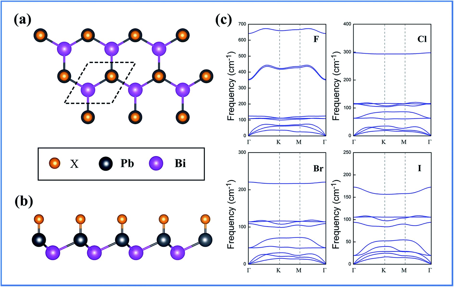 | ||
| Fig. 1 (a) Top view and (b) side view of the BiPbX (X = F, Cl, Br, and I) monolayer, and (c) phonon band dispersions of BiPbX. | ||
| Structure | a (Å) | h (Å) | dBi–Pb (Å) | dPb–X (Å) | ΔEf (eV) | Eg (eV) | EΓ (eV) | Eg-SOC (eV) | EΓ-SOC (eV) | Z2 |
|---|---|---|---|---|---|---|---|---|---|---|
| BiPbF | 4.78 | 1.28 | 3.04 | 2.06 | −2.64 | 0.217 | 0.217 | 0.232 | 0.278 | 1 |
| BiPbCl | 4.75 | 1.32 | 3.04 | 2.46 | −1.28 | 0.195 | 0.195 | 0.229 | 0.275 | 1 |
| BiPbBr | 4.73 | 1.34 | 3.04 | 2.60 | −1.13 | 0.163 | 0.163 | 0.196 | 0.288 | 1 |
| BiPbI | 4.72 | 1.35 | 3.04 | 2.81 | −0.88 | 0.071 | 0.071 | 0.138 | 0.320 | 1 |
To test the thermostability of the BiPbX monolayers, we performed first-principles molecular dynamics (MD) simulations. We used a 4 × 4 supercell and carried out the individual MD simulations for BiPbBr as an example. As can be seen from Fig. 2, the structure of the BiPbBr monolayer does not collapse throughout a 5 ps MD simulation up to 300 K, indicating that the melting point of the BiPbBr monolayer is probably 300 K. The abovementioned results reveal that the BiPbBr monolayer has a very good thermal stability and can maintain its structural integrity at high temperatures.
 | ||
| Fig. 2 Total potential energy fluctuations during the MD simulations at 300 K for the BiPbBr monolayer. | ||
The calculated band structures for BiPbX with X = (F, Cl, Br, and I) are shown in Fig. 3, where the red and blue dots represent the pz and px,y states, respectively. Without including SOC effects, they exhibit semiconducting character, with the valence band maximum (VBM) and the conduction band minimum (CBM) degenerating at the Γ point. Upon increasing the atomic number of the halogen in the PbX dimer, the band gap continuously decreases, reaching 71 meV for the PbI dimer. When including SOC effects, the CBM, which is mainly occupied by pz orbitals, is pushed downwards, whereas the VBM, which is occupied by px,y orbitals, is reversely pushed upwards. Due to the strong SOC effects of the Bi and Pb atoms, the band order around the Γ point is inverted, leading to the appearance of a Mexican hat shape near the VBM, which is opposite to the band state alignment without including the SOC effects. This px,y–pz band inversion strongly indicates the topologically nontrivial nature of these films. To overcome the possible underestimation of the band gap, we also employed the HSE06 functional to check the existence of band inversion, as shown in Fig. 4. Note that the nontrivial band gap is enlarged to 0.53–0.72 eV, which is larger than that of Bi(111) (0.2 eV),14 ZrTe5 (0.1 eV),56 as well as stanene (0.1 eV).13 The large nontrivial band gap of these monolayers is very favourable for future experimental applications and makes them highly adaptable to various application fields.
 | ||
| Fig. 3 Orbital-resolved band structures of (a) BiPbF, (b) BiPbCl, (c) BiPbBr, and (d) BiPbI, without SOC and with SOC effects. | ||
 | ||
| Fig. 4 Calculated band structures of the BiPbBr monolayer by the HSE06 functional (a) without SOC and (b) with SOC effects. | ||
The hallmark of the QSH effect is the helical edge state, which is the key to spintronics due to their ability to conduct dissipationless currents. To explicitly see these topological features, the edge Green's functions were calculated by the ab initio tight-binding (TB) model, with the recursive method in terms of maximally localized Wannier functions (MLWFs).57 As the energy bands near the Fermi level are predominantly composed of hybridized pz and px,y orbitals, the MLWFs are mainly composed of p-like atomic orbitals. Fig. 5(b)and (c) display the bands fitted by the DFT and TB model, as well as the local density of states (LDOS) on the edge states. The good fitting confirms the validity of our results. Obviously, all the edge bands completely connect the conduction and valence bands and span the 2D bulk band gap, yielding 1D gapless edge states. Furthermore, the band topology was evaluated by the Z2 topological invariant. Due to the inversion-symmetry breaking, the Z2 invariant can be obtained to trace the Wannier Center of Charges (WCCs) using a non-Abelian Berry connection.58 By counting the number of crossings of any arbitrary horizontal reference line, it was found that the WCCs evolution curves cross any arbitrary reference lines in odd number of times, yielding Z2 = 1, as shown in Fig. 5(a).
 | ||
| Fig. 5 (a) Evolution of the Wannier centers along ky. The evolution lines cross the arbitrary reference line (red dashed line parallel to ky) an odd number of times. (b) Comparison of the band structures obtained by DFT (red circles) and the Wannier function (blue lines). (c) Topological edge states of the BiPbCl monolayer with SOC effects, as obtained by the ab initio TB Wannier function. | ||
Then, we focused on the origin of the QSH effect in these systems. As abovementioned, the hybridization of halogen atoms with Pb-pz orbital occurs in the PbX dimers, the pz band is shifted away from the Fermi level, leaving only Pb-px,y orbitals and Bi-pz orbitals, as displayed in Fig. 3. Thus, the evolution of the atomic orbitals can be summarized in three stages: (I), (II), and (III), as shown in Fig. 6(a). In stage (I), the crystal field makes the p states split into both px,y and pz orbitals due to C3 symmetry, with pz shifting upwards with respect to the degenerate px,y orbitals. When chemical bonding occurs between Bi and PbX dimer, in stage (II), the states near the Fermi level are further split into bonding and anti-bonding states, i.e., px,y+, px,y,z+, px,y− and pz−, where the superscripts + and − represent the parities of the corresponding states. When considering the SOC effects, in stage III, the strong SOC effects drive the pz+ and px,y− states to exchange positions near the Fermi level, leading to a band inversion. Note that this mechanism is different from that of ZrTe5/HfTe5, 1T-MX2 and 1T′-MoX2, where the SOC effects do not cause a change in the band order, whereas only a sizable gap is opened at the Fermi level. To confirm these observations, we artificially added a scaling factor λ in front of the SOC term in the calculations, gradually increasing the strength of the SOC effects from zero to its full value and monitoring the evolution of the band structure. Taking BiPbF as an example, in Fig. 6(b) and (c), it can be observed that the direct band gap at the Γ point decreases to zero at a critical value λ = 0.48, and then it reopens again, finally reaching a value of 0.28 eV at λ = 1.0. Obviously, the topological phase transition in the current system is driven by the strength of the SOC effects, which is in agreement with the abovementioned band order analysis.
 | ||
| Fig. 6 (a) Schematic of the evolution from atomic Bi pz orbitals and Bi–Pb px,y orbitals into the conduction and valence bands at the Γ point. (b) Changes in the band gap at the Γ point of the BiPbF monolayer as a function of SOC strength. (c) Band structures with respect to the SOC strength with λ = 0%, 20%, 48%, 70%, and 100%. | ||
Another prominent feature of these films is that if the SOC effects are included, the energy bands at the Fermi level are spin-split, which is a signature of Rashba spin splitting (RSS). Fig. 7 presents the spin texture for the highest valence bands of all BiPbX films, where, indeed, the spin components projected to the in-plane polarization are normal to k in the Brillouin zone. The RSS is characterized by the Rashba energy ER and the corresponding momentum offset ΔkR away from the crossing point, which is illustrated in the inset of Fig. 7(a). From an estimation of ΔkR and a fitting value of the effective mass, we found that the effective Rashba constant αR = ħ2ΔK/m* reaches a value as large as 0.29 eV Å−1, larger than the results obtained for InGaAs/GaAs quantum dots (αR ∼ 0.08–0.12 eV Å−1)59 or InGaAs/InAlAs quantum wells (αR = 0.07 eV Å−1).60 The larger RSS in the electronic bands obtained herein provides a platform for spintronic device applications without applying a magnetic field, for instance, in spin field-effect transistors (FET).
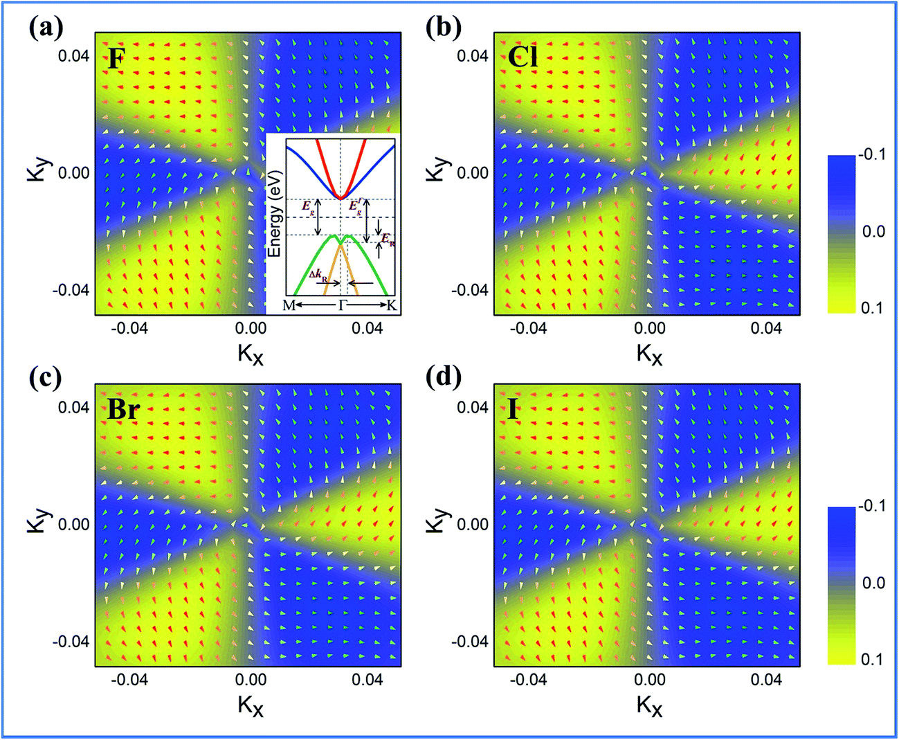 | ||
| Fig. 7 Spin texture in the highest valence bands for (a) BiPbF, (b) BiPbCl, (c) BiPbBr, and (d) BiPbI monolayer. Arrows refer to the in-plane orientation of the spins, and the background color denotes the z component of the spins. The inset in (a) is the enlarged view of the bands around the Fermi level at the Γ point for the BiPbF structure. | ||
Strain engineering is an efficient way of modulating the electronic and topological properties of 2D films. A biaxial strain can be applied by adjusting the in-plane lattice parameters, i.e., ε = (a − a0)/a0, where a and a0 are the strained and unstrained lattice constants, respectively. The calculated results are illustrated in Fig. 8. The large bulk band gap and sizable Rashba splitting coexist in all the cases. Quite interestingly, the Rashba splitting is tunable over a wide range of strains (−2–14%), with the maximum bulk band gap being enhanced to 81 meV, whereas the bulk band gap remains large enough (0.04–0.36 eV).
 | ||
| Fig. 8 Variations of the global band gap (Eg), band gap at the Γ point (EgΓ) and RSS (ER) as a function of external strain for (a) BiPbF, (b) BiPbCl, (c) BiPbBr, (d) BiPbI monolayers. | ||
Finally, as illustrated in Fig. 9(a), we constructed a BiPbH/h-BN heterostructure (HTS) using BN as a substrate, where the lattice of h-BN matches well with the lattice of the BiPbF monolayer. After full relaxation with van der Waals (vdW) forces,61 the distance (d) between adjacent layers is 4.1 Å, with the binding energy being −75 meV, suggesting a typical vdW HTS. Fig. 9(b) presents the band structures with and without SOC effects. It can be observed that a few bands appear within the bulk band gap of the h-BN substrate around the Fermi level, which is mainly contributed by orbitals from the BiPbF films, according to the wave-function analysis. Upon projecting Bloch wave functions onto the atomic orbitals, the px,y–pz band order inversion occurs. Therefore, the BiPbX monolayer supported on the h-BN substrate is a robust TI.
 | ||
| Fig. 9 (a) Schematic with a top and side view of the epitaxially grown BiPbF layer on a h-BN (0001) substrate and (b) band structures without SOC and with SOC effects for the BiPbF/h-BN (0001) HTS. | ||
In summary, we proposed a new type of 2D TIs based on the films consisting of group IV–V–VI elements, which exhibit a giant Rashba spin splitting, due to their peculiar polar atomic structure. The coexistence of the topological band gap and Rashba splitting is stable over a wide range of strain (−2–14%), with even the maximum bulk band gap being enhanced to 0.36 eV, which is important for room-temperature realization of QSH states. Considering the robustness of the topologically nontrivial band structure with a h-BN substrate, this study opens a route for the design of topological spintronic devices based on the films consisting of 2D group IV–V–VI elements.
Acknowledgements
This work was supported by the National Natural Science Foundation of China (Grant No. 11434006, 61172028, and 11304121).References
- S. Datta and B. Das, Appl. Phys. Lett., 1990, 56, 665–667 CrossRef CAS.
- P. Gambardella and I. M. Miron, Philos. Trans. R. Soc., A, 2011, 369, 3175–3197 CrossRef CAS PubMed.
- Y. A. Bychkov and E. I. Rashba, J. Phys. C: Solid State Phys., 1984, 17, 6039–6045 CrossRef.
- D. Awschalom and N. Samarth, Physics, 2009, 2, 50 CrossRef.
- C. Tahan and R. Joynt, Phys. Rev. B: Condens. Matter Mater. Phys., 2005, 71, 075315 CrossRef.
- D. Popović, F. Reinert, S. Hüfner, V. G. Grigoryan, M. Springborg, H. Cercellier, Y. Fagot-Revurat, B. Kierren and D. Malterre, Phys. Rev. B: Condens. Matter Mater. Phys., 2005, 72, 045419 CrossRef.
- A. Varykhalov, D. Marchenko, M. R. Scholz, E. D. L. Rienks, T. K. Kim, G. Bihlmayer, J. Sánchez-Barriga and O. Rader, Phys. Rev. Lett., 2012, 108, 066804 CrossRef CAS PubMed.
- Y. M. Koroteev, G. Bihlmayer, J. E. Gayone, E. V. Chulkov, S. Blügel, P. M. Echenique and P. Hofmann, Phys. Rev. Lett., 2004, 93, 046403 CrossRef PubMed.
- K. Sugawara, T. Sato, S. Souma, T. Takahashi, M. Arai and T. Sasaki, Phys. Rev. Lett., 2006, 96, 046411 CrossRef CAS PubMed.
- C. R. Ast, J. Henk, A. Ernst, L. Moreschini, M. C. Falub, D. Pacilé, P. Bruno, K. Kern and M. Grioni, Phys. Rev. Lett., 2007, 98, 186807 CrossRef PubMed.
- S. Mathias, A. Ruffing, F. Deicke, M. Wiesenmayer, I. Sakar, G. Bihlmayer, E. V. Chulkov, Y. M. Koroteev, P. M. Echenique and M. Bauer, Phys. Rev. Lett., 2010, 104, 066802 CrossRef CAS PubMed.
- K. Ishizaka, M. S. Bahramy, H. Murakawa, M. Sakano, T. Shimojima, T. Sonobe, K. Koizumi, S. Shin, H. Miyahara and A. Kimura, Nat. Mater., 2011, 10, 521–526 CrossRef CAS PubMed.
- D. Di Sante, P. Barone, R. Bertacco and S. Picozzi, Adv. Mater., 2013, 25, 509–513 CrossRef CAS PubMed.
- M. Kepenekian, R. Robles, C. Katan, D. Sapori, L. Pedesseau and J. Even, ACS Nano, 2015, 9, 11557–11567 CrossRef CAS PubMed.
- Q. H. Liu, X. W. Zhang, L. B. Abdalla and A. Zunger, Adv. Funct. Mater., 2016, 26, 3259–3267 CrossRef CAS.
- J. E. Moore, Nature, 2010, 464, 194–198 CrossRef CAS PubMed.
- M. Z. Hasan and C. L. Kane, Rev. Mod. Phys., 2010, 82, 3045–3067 CrossRef CAS.
- X. L. Qi and S. C. Zhang, Rev. Mod. Phys., 2011, 83, 1057–1110 CrossRef CAS.
- H. J. Zhang, C. X. Liu, X. L. Qi, X. Dai, Z. Fang and S. C. Zhang, Nat. Phys., 2009, 5, 438–442 CrossRef CAS.
- Y. L. Chen, J. G. Analytis, J. H. Chu, Z. K. Liu, S. K. Mo, X. L. Qi, H. J. Zhang, D. H. Lu, X. Dai, Z. Fang, S. C. Zhang, I. R. Fisher, Z. Hussain and Z. X. Shen, Science, 2009, 325, 178–181 CrossRef CAS PubMed.
- Y. Xia, D. Qian, D. Hsieh, L. Wray, A. Pal, H. Lin, A. Bansil, D. Grauer, Y. S. Hor, R. J. Cava and M. Z. Hasan, Nat. Phys., 2009, 5, 398–402 CrossRef CAS.
- T. Zhang, P. Cheng, X. Chen, J. F. Jia, X. Ma, K. He, L. Wang, H. Zhang, X. Dai, Z. Fang, X. Xie and Q. K. Xue, Phys. Rev. Lett., 2009, 103, 266803 CrossRef PubMed.
- B. A. Bernevig, T. L. Hughes and S. C. Zhang, Science, 2006, 314, 1757 CrossRef CAS PubMed.
- M. König, S. Wiedmann, C. Brüne, A. Roth, H. Buhmann, L. W. Molenkamp, X. L. Qi and S. C. Zhang, Science, 2007, 318, 766–770 CrossRef PubMed.
- A. Roth, C. Brüne, H. Buhmann, L. W. Molenkamp, J. Maciejko, X. L. Qi and S. C. Zhang, Science, 2009, 325, 294–297 CrossRef CAS PubMed.
- C. Liu, T. L. Hughes, X. L. Qi, K. Wang and S. C. Zhang, Phys. Rev. Lett., 2008, 100, 236601 CrossRef PubMed.
- C. C. Liu, W. Feng and Y. Yao, Phys. Rev. Lett., 2011, 107, 076802 CrossRef PubMed.
- Y. Xu, B. Yan, H. J. Zhang, J. Wang, G. Xu, P. Tang, W. Duan and S. C. Zhang, Phys. Rev. Lett., 2013, 111, 136804 CrossRef PubMed.
- Y. P. Wang, C. W. Zhang, W. X. Ji, M. J. Ren, X. L. Chen, M. Yuan and P. J. Wang, J. Phys. D: Appl. Phys., 2016, 49, 055305 CrossRef.
- Z. Liu, C. X. Liu, Y. S. Wu, W. H. Duan, F. Liu and J. Wu, Phys. Rev. Lett., 2011, 107, 136805 CrossRef PubMed.
- F. C. Chuang, L. Z. Yao, Z. Q. Huang, Y. T. Liu, C. H. Hsu, T. Das, H. Lin and A. Bansil, Nano Lett., 2014, 14, 2505–2508 CrossRef CAS PubMed.
- W. Luo and H. J. Xiang, Nano Lett., 2015, 15, 3230–3235 CrossRef CAS PubMed.
- J. J. Zhou, W. Feng, C. C. Liu, S. Guan and Y. Yao, Nano Lett., 2014, 14, 4767–4771 CrossRef CAS PubMed.
- W. W. Zhao, X. Chen, L. Y. Li and X. M. Zhang, Sci. Rep., 2015, 5, 8441 CrossRef PubMed.
- L. Y. Li, X. M. Zhang, X. Chen and M. W. Zhao, Nano Lett., 2015, 15, 1296 CrossRef CAS PubMed.
- A. Z. Wang, Z. H. Wang, A. J. Du and M. W. Zhao, Phys. Chem. Chem. Phys., 2016, 18, 22154 RSC.
- Y. P. Wang, C. W. Zhang, W. X. Ji, P. Li, P. J. Wang and S. S. Yan, Appl. Phys. Lett., 2016, 108, 073104 CrossRef.
- Y. Ma, Y. Dai, L. Kou, T. Frauenheim and T. Heine, Nano Lett., 2015, 15, 1083 CrossRef CAS PubMed.
- R. W. Zhang, C. W. Zhang, W. X. Ji, S. S. Li, S. J. Hu, S. S. Yan, P. Li, P. J. Wang and F. Li, New J. Phys., 2015, 17, 083036 CrossRef.
- H. Zhao, C. W. Zhang, W. X. Ji, R. W. Zhang, S. S. Li, S. S. Yan, B. M. Zhang, P. Li and P. J. Wang, Sci. Rep., 2016, 6, 20152 CrossRef CAS PubMed.
- R. W. Zhang, C. W. Zhang, W. X. Ji, S. S. Li, S. S. Yan and P. J. Wang, Sci. Rep., 2016, 6, 21351 CrossRef CAS PubMed.
- Y. P. Wang, W. X. Ji, C. W. Zhang, P. Li, F. Li, M. J. Ren, X. L. Chen, M. Yuan and P. J. Wang, Sci. Rep., 2016, 6, 20342 CrossRef CAS PubMed.
- Y. Z. Jia, W. X. Ji, C. W. Zhang, P. Li, M. J. Ren and P. J. Wang, J. Mater. Chem. C, 2016, 4(37), 8750–8757 RSC.
- R. W. Zhang, C. W. Zhang, W. X. Ji, P. Li, P. J. Wang, S. S. Li and S. S. Yan, Appl. Phys. Lett., 2016, 109, 182109 CrossRef.
- R. W. Zhang, C. W. Zhang, W. X. Ji, S. S. Li, S. S. Yan, S. J. Hu, P. Li and P. J. Wang, J. Mater. Chem. C, 2016, 4, 2088 RSC.
- X. Wan, A. M. Turner, A. Vishwanath and S. Y. Savrasov, Phys. Rev. B: Condens. Matter Mater. Phys., 2011, 83, 205101 CrossRef.
- J. Wang, X. Chen, B. F. Zhu and S. C. Zhang, Phys. Rev. B: Condens. Matter Mater. Phys., 2012, 85, 235131 CrossRef.
- G. Kresse and J. Furthmüller, Phys. Rev. B: Condens. Matter Mater. Phys., 1996, 54, 11169–11186 CrossRef CAS.
- G. Kresse and J. Hafner, Phys. Rev. B: Condens. Matter Mater. Phys., 1994, 49, 14251–14269 CrossRef CAS.
- G. Kresse and D. Joubert, Phys. Rev. B: Condens. Matter Mater. Phys., 1999, 59, 1758–1775 CrossRef CAS.
- J. P. Perdew and Y. Wang, Phys. Rev. B: Condens. Matter Mater. Phys., 1992, 45, 13244–13249 CrossRef.
- J. Heyd, G. E. Scuseria and M. Ernzerhof, J. Chem. Phys., 2006, 124, 219906 CrossRef.
- J. Heyd, G. E. Scuseria and M. Ernzerhof, J. Chem. Phys., 2003, 118, 8207 CrossRef CAS.
- C. W. Zhang and S. S. Yan, J. Phys. Chem. C, 2012, 116, 4163–4166 CAS.
- F. B. Zheng and C. W. Zhang, Nanoscale Res. Lett., 2012, 7, 422 CrossRef PubMed.
- H. Weng, X. Dai and Z. Fang, Phys. Rev. X, 2014, 4(1), 011002 Search PubMed.
- M. P. Lopez Sancho, J. M. Lopez Sancho, J. M. L. Sancho and J. Rubio, J. Phys. F: Met. Phys., 1985, 15, 851 CrossRef.
- R. Yu, X. L. Qi, A. Bernevig, Z. Fang and X. Dai, Phys. Rev. B: Condens. Matter Mater. Phys., 2011, 84, 075119 CrossRef.
- S. M. Huang, A. O. Badrutdinov, L. Serra, T. Kodera, T. Nakaoka, N. Kumagai, Y. Arakawa, D. A. Tayurskii, K. Kono and K. Ono, Phys. Rev. B: Condens. Matter Mater. Phys., 2011, 84, 085325 CrossRef.
- J. Nitta, T. Akazaki, H. Takayanagi and T. Enoki, Phys. Rev. Lett., 1997, 78, 1335–1338 CrossRef CAS.
- J. Klimeš, D. R. Bowler and A. Michaelides, Phys. Rev. B: Condens. Matter Mater. Phys., 2011, 83, 195131 CrossRef.
| This journal is © The Royal Society of Chemistry 2017 |