DOI:
10.1039/C6RA28752B
(Paper)
RSC Adv., 2017,
7, 15885-15893
Single step fabrication of CuO–MnO–2TiO2 composite thin films with improved photoelectrochemical response†
Received
27th December 2016
, Accepted 6th March 2017
First published on 10th March 2017
1. Introduction
Due to global warming, finite fossil fuel resources and an exponential increase in world population, the need to develop clean, benign and infinite energy rich sources is being brought into ever sharper focus. Hydrogen generation from photoelectrochemical (PEC) water splitting is an attractive ‘alternate way’ to make solar energy storable and transportable1–5 since Fujishima and Honda reported PEC water splitting using a TiO2 electrode.6 Several semiconducting nanostructured materials such as perovskite structured organometallic compounds, metal oxides, dye sensitized solar cells, metal composites and solid solutions and polymer-based materials have been tested for this purpose.7 Multi-metal oxide nanocomposite materials such as CuO–Al2O3–TiO2,8 CeO2–CuO–ZnO,9 CeO–ZnO–ZnAl2O3,10 ZnO–TiO2–SnO2 11 have drawn intensive attention in recent times. The properties which arise from their combination make the materials potentially important and are not necessarily observed in the single individual components. Studies have revealed that within a mixed metal oxide system redistribution of charge, new electronic states, charge transfer transition between conduction and valence band of the semiconducting oxide takes place thereby causing a decrease in band gap energy.12 These composite materials via synergistic effect of multi-metal semiconducting system improve interfacial charge transfer and thereby minimizing charge recombination for enhanced PEC performance.13 Transition multi-metal metal oxide semiconductors have found a wide range of applications as functional materials in the fields of microelectronic devices,14,15 ceramics,16 catalysis,17 nonlinear optical,18 PEC applications19 and semiconductor devices.20
Several physical and chemical techniques have been adopted for the fabrication of mixed metal oxide thin films21–27 nevertheless based on our previous experience, we chose solution-based aerosol assisted chemical vapour deposition (AACVD) technique. Thin films produced by AACVD afford inexpensive, adhesive, reproducible films with low impurity levels, excellent film uniformity, high deposition rates, controllability of film microstructure and scalability.28 Further we found that trifluoroacetato has strong tendency to replace relatively weaker acetate ligand in metal acetates to form trifluoro complexes that have matching solubility and thermal properties suitable for their conversion to metal oxides. Moreover trifluoro ligand has also ability to bind two or more metals in one structure to yield molecular complex that are most suitable precursors to chemical vapour deposition. Here in we treated (Cu(CH3COO)2·H2O), (Mn(CH3COO)2) and (Ti(O(CH2)3CH3)4) with TFA in tetrahydrofuran (THF) to convert them into respective metal trifluoroacetates and utilized this mixture for the fabrication of well adhered and uniform CuO–MnO–2TiO2 composite thin films on the FTO substrate applying AACVD at 550 °C. The crystallinity, phase orientation, stoichiometry, surface morphology, optical properties and oxidation states of involved atoms were determined by X-ray diffraction (XRD), energy dispersive X-ray (EDX), field emission scanning electron microscopy (FESEM), ultraviolet-visible (UV-vis) spectroscopy and X-ray photoelectron spectroscopy (XPS), respectively. The scope of these thin film electrodes towards PEC for the generation of photoelectric current was studied by linear scanning voltammetry (LSV) and the charge transfer dynamics of the thin films were investigated by electrochemical impedance spectroscopic (EIS) technique.
2. Experimental
2.1. Chemicals and reagents
All manipulations were carried out under an inert atmosphere of dry argon using Schlenk tube fitted with vacuum line and hot plate/magnetic stirrer arrangements. The solvent was rigorously dried over sodium benzophenoate and distilled immediately before use. (Cu(CH3COO)2·H2O), (Mn(CH3COO)2), (Ti(O(CH2)3CH3)4) and TFA were purchased from Sigma-Aldrich. The reagents were used as received. Fluorine doped tin oxide (FTO) conducting glass slides with surface resistivity of 8 Ω sq−1 were also supplied by Sigma-Aldrich.
2.2. Fabrication of CuO–MnO–2TiO2 composite thin films by AACVD technique
The CuO–MnO–2TiO2 thin films were fabricated using self-designed aerosol assisted chemical vapor deposition assembly29 onto FTO glass substrate. Prior to the deposition, the FTO glass slides with dimensions of 25.4 × 12.7 × 2.2 mm (L × W × D) were ultrasonically cleaned sequentially using distilled water, acetone, and then ethyl alcohol. Finally, they were washed with distilled water, stored in ethanol, and dried in air. Substrate slides of the dimension of 25.4 mm × 12.7 mm were placed inside the reactor tube and then heated up to the deposition temperature 550 °C for 10 min to stabilize the temperature before carrying out the deposition. The aerosols of the solution were formed by keeping the round bottom flask in a water bath above the piezoelectric modulator of an ultrasonic humidifier. The generated aerosol droplets of the solution were transferred into the hot wall zone of the reactor by argon gas. The exhaust from the reactor was vented directly into the extraction system of a fume cupboard. At the end of the deposition, the aerosol line was closed and only carrier gas was allowed to pass over the substrate. The substrate was allowed to cool to 30 °C before it was taken out from the reactor.
In a typical deposition experiment, 0.10 g (0.58 mmol) of Mn(CH3COO)2, 0.11 g (0.58 mmol) of Cu(CH3COO)2·H2O and 0.4 mL (1.16 mmol) of Ti(O(CH2)3CH3)4 was added in 100 mL Schlenk tube containing 15 mL THF. The mixture was stirred for about 2 hours followed by the addition of TFA to yield a clear solution which was evaporated under vacuum to give green coloured powder. This powder was re-dissolved in THF filtered through cannula and was used for the fabrication of CuO–MnO–2TiO2 thin films at 550 °C for 45 minutes. The carrier gas at a flow rate of 120 mL min−1 was controlled by a L1X linear flow meter. The deposited light green thin films are transparent, uniform, robust, and stable towards atmospheric conditions and adhere strongly on FTO substrate as verified by the “scotch tape test”.
2.3. Material characterization techniques
The crystalline phase of the sample was analyzed by XRD measurements by using a PANanalytical, X'PertHighScore diffractometer with primary monochromatic high intensity CuKα (λ = 1.5418 Å) radiation over Bragg angles ranging from 10 to 90° in a step size of 0.026°, at a voltage of 40 kV and current of 40 mA at ambient temperature. The FT-IR spectra was recorded on a single reflectance ATR instrument (4000–450 cm−1 with a resolution of 4 cm−1). Raman spectroscopic measurements of the films were carried out on a Renishaw InVia Raman microscope and excitation was performed using the 514 nm line of argon laser with a 0.01 mW output power. The surface morphology of thin films was studied using a field emission scanning electron microscope, FEI Quanta 400 coupled with energy dispersive X-ray spectrometer (EDX) (INCA Energy 200 (Oxford Inst.)), at an accelerating voltage of 20 kV, 80![[thin space (1/6-em)]](https://www.rsc.org/images/entities/char_2009.gif) 000 magnification and a working distance of 9 mm. The optical absorption properties of the thin films were recorded on Lambda 35 Perkin-Elmer UV-Vis spectrophotometer in the spectral region of 330–900 nm using similar FTO coated glass substrate as a reference to eliminate the substrate impact in the spectrum. The thickness of the films was measured using a profilometer KLA Tencore P-6 surface profiler. XPS analysis of the films was carried out using an ULVAC-PHI Quantera II with a 32-channel Spherical Capacitor Energy Analyzer under vacuum (1 × 10⁻⁶ Pa) using monochromatic Al Kα radiation (1486.8 eV) and a natural energy width of 680 meV. The carbonaceous C 1s line (284.6 eV) was used as a reference to calibrate the binding energies.
000 magnification and a working distance of 9 mm. The optical absorption properties of the thin films were recorded on Lambda 35 Perkin-Elmer UV-Vis spectrophotometer in the spectral region of 330–900 nm using similar FTO coated glass substrate as a reference to eliminate the substrate impact in the spectrum. The thickness of the films was measured using a profilometer KLA Tencore P-6 surface profiler. XPS analysis of the films was carried out using an ULVAC-PHI Quantera II with a 32-channel Spherical Capacitor Energy Analyzer under vacuum (1 × 10⁻⁶ Pa) using monochromatic Al Kα radiation (1486.8 eV) and a natural energy width of 680 meV. The carbonaceous C 1s line (284.6 eV) was used as a reference to calibrate the binding energies.
2.4. Photo-electrochemical measurement
The photo-electrochemical response of the fabricated CuO–MnO–2TiO2 composite thin film was studied using Linear Scan Voltammetry (LSV) technique with Princeton Applied Research (PAR-VersaSTAT-3) electrochemical workstation in a conventional three-electrode system. The I–V characteristics were performed (potential window range: −0.2 to +1.2 V, and scan rate: 50 mV s−1) using the fabricated thin film electrode as the working electrode, while the reference, counter electrodes were Ag/AgCl (KCl) and platinum wire, respectively. For the photocurrent measurement, the fabricated thin film electrode was inserted into the quartz window cell containing 0.5 M Na2SO4 aqueous solution in the dark and irradiated with a 150 W xenon arc lamp (Newport, Model 69907) containing a simulated AM 1.5 G filter. The EIS measurements of the thin films were carried out using a computer-controlled Princeton Applied Research (PAR-VersaSTAT 3) electrochemical workstation. The amplitude potential was 5 mV around the open circuit potential, with a frequency range of 0.1 Hz to 10 kHz.
3. Results and discussions
3.1. X-ray diffraction studies
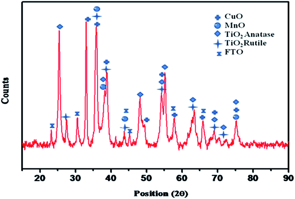
Fig. 1 shows the X-ray diffractogram of the CuO–MnO–2TiO2 thin film deposited on FTO glass substrate at 550 °C using THF solution of initial precursors by the AACVD technique. XRD qualitative analysis was performed on X-ray diffractogram which reveals the growth of tenorite CuO (ICDD 00-002-1041), MnO (ICDD 00-004-0326) and a mixture of anatase (ICDD 00-002-0387) and rutile (ICDD 01-075-1748) TiO2 phases as crystalline end product. CuO exhibits monoclinic crystal system with space group C2/c, cell parameters of a = 4.65, b = 3.41, c = 5.11 Å and produced characteristic peaks indicated by (+) at 2θ = 32.41, 35.59, 39.13, 49.21, 53.88, 58.35, 66.22, 68.45 and 75.37° as observed by their Miller indices (110), (002), (200), (−202), (020), (202), (022), (220), (004) respectively. MnO has orthorhombic crystal system and cell parameters a = 4.42, b = 10.40, c = 2.83 Å. The characteristic peaks of MnO indicated by (●) at 2θ = 36.35, 38.35, 43.71, 74.67 originate from their Miller indices (021), (111), (050), (321) respectively. The emergence of peaks at 2θ = 25.35 (101), 37.93 (004), 38.61 (112), 48.10 (200), 53.88 (105), 55.29 (211), 68.99 (116), 70.17 (220), 75.37 (215) denoted by (◆) are well indexed to tetragonal anatase TiO2. Furthermore, the peaks marked by ( ) at 2θ = 27.43 (110), 36.07 (011), 39.18 (020), 54.31 (121), 65.50 (221), 68.99 (031) are attributed to tetragonal rutile TiO2. The rest of reflections are assigned to FTO substrate (ICDD card no. [00-007-0195]). Sticky pattern matching is available in (Fig. S1†).
 |
| | Fig. 1 X-ray diffractogram of the as-grown CuO–MnO–2TiO2 composite thin film fabricated on FTO substrate at deposition temperature of 550 °C for 45 minutes under Ar atmosphere. | |
3.2. FT-IR and Raman spectroscopy
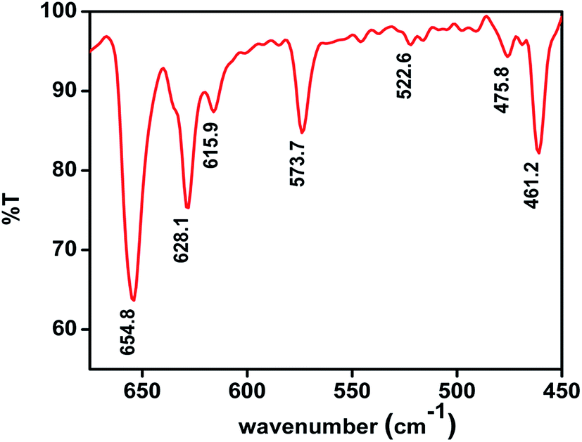
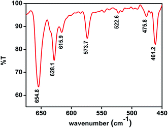
The FT-IR spectra of CuO–MnO–2TiO2 composite thin films were recorded in the range of 450–4000 cm−1 is shown in Fig. 2. For CuO, the vibrational modes were observed at 461.2 cm−1, 475.8 cm−1, 522.6 cm−1, 573.7 cm−1, 615.9 cm−1.30–33 The weak features located at low frequency mode may be attributed to the Cu–O symmetric and asymmetric stretching. The high frequency mode (Cu–O wagging) imply the presence of metal oxide group in the sample. Strong peak at about 628.1 cm−1 arise from the stretching vibration of Mn–O indicating the formation of MnO.34 Peak observed at 654.8 cm−1 indicate Ti–O vibration.35
 |
| | Fig. 2 FT-IR spectrum of CuO–MnO–2TiO2 composite. | |
Further the structural analysis of CuO–MnO–2TiO2 composite thin films was carried out by Raman spectroscopy and results are displayed in Fig. 3. The Raman scattering vibration modes detected at 149, 198, 405, 516 and 655 cm−1, corresponds to anatase TiO2 phase,36,37 peaks at 365 and 655 cm−1 attributes to MnO phase38 and peaks located at 285, 340 and 618 cm−1 represents the presence of CuO phase.36,37 These observations are in good agreement with that determined from the FT-IR measurements. In general, the mixed oxide spectrum has significantly changed in the range of 400–1000 cm−1 due to the addition of crystalline phases. The characteristic peaks for rutile TiO2 which are expected to appear at 246, 446 and 601 cm−1 are merged in the broad bands at 285, 405 and 630 cm−1. Hence the CuO, MnO and mixture of anatase and rutile TiO2 phases determined from our XRD analysis are further validated from Raman spectroscopy.
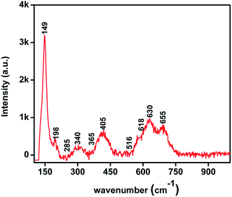 |
| | Fig. 3 Raman spectra of CuO–MnO–2TiO2 composite. | |
3.3. Surface morphology
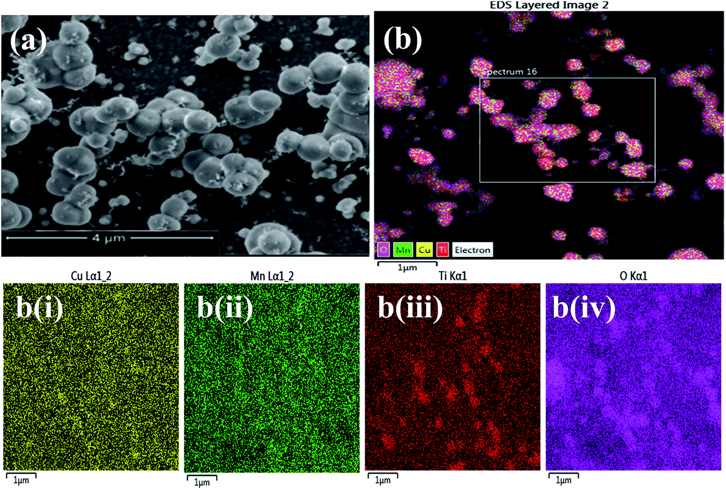
The surface morphology of CuO–MnO–2TiO2 composite film developed at 550 °C via AACVD was examined by FESEM analysis. Fig. 4a shows the surface topography of the film prepared from THF solution is composed of interconnected heterogeneous spherical shaped nanoballs which are stacked in the vertical direction of substrate plane. One type of microspherical object attains donuts shape structure while the other exists as round ball shaped. The low resolution surface SEM image (Fig. S2†) reveal these microspherical objects are homogenously distributed though out the film matrix. We believe that the film growth by AACVD technique involves a homogeneous and heterogeneous reaction. The interaction between homogeneous and heterogeneous processes depends on the physical properties such as the boiling point, density, surface tension and heat of combustion of the solvent. Solvents with lower boiling point and higher heat of combustion yield thin films via a homogeneous process, while solvents with higher boiling point and lower heat of combustion contribute to the heterogeneous process, during the film formation.39 It has been observed that the film formation was influenced by both the homogeneous and heterogeneous process, but with a greater tendency toward the homogeneous process in the THF solvent.
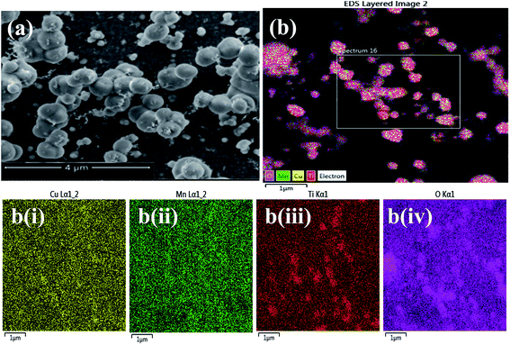 |
| | Fig. 4 (a) FESEM image of CuO–MnO–2TiO2 composite thin film deposit on FTO substrate by AACVD, (b) EDX elemental map showing the distribution of Cu, Mn, Ti and O in CuO–MnO–2TiO2 composite thin film, b(i), b(ii), b(iii) and b(iv) representing EDX mapping of Cu, Mn, Ti and O respectively. | |
The elemental composition of CuO–MnO–2TiO2 composite thin film was analyzed by energy dispersive X-ray (EDX) analysis and spectras are presented in (Fig. S3†). The EDX analysis executed on several randomly selected regions reveal that the metallic ratio of Cu:Mn:Ti in the film is close to 1:1:2 confirming maintenance of the same metallic ratio in the film as in the original solution. Further the color scheme in EDX map analysis (Fig. 4b(i–iv)) helped in assurance of uniform distribution of individual atoms with a fixed ratio throughout the composite matrix of CuO–MnO–2TiO2.
3.4. XPS analysis
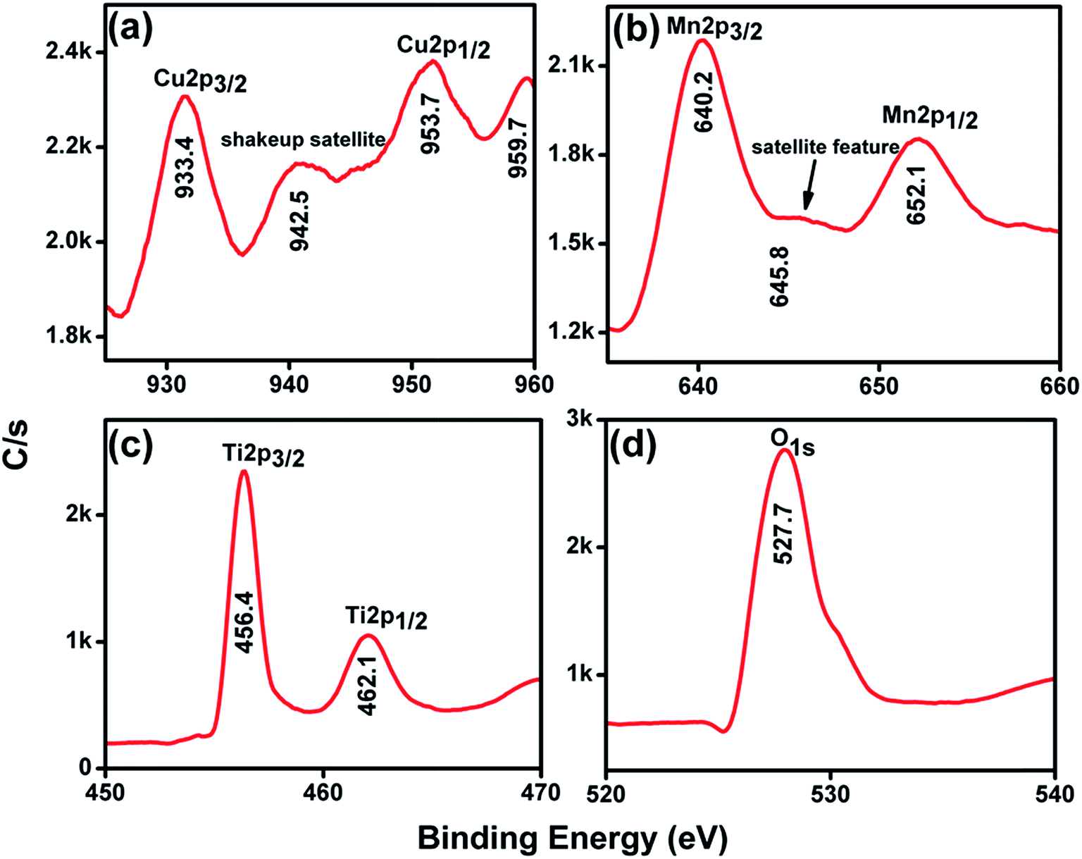
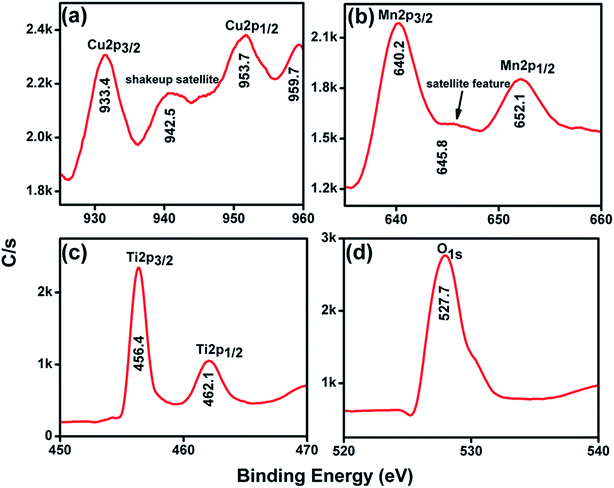
The CuO–MnO–2TiO2 composite film was employed in X-ray photoelectron spectroscopy (XPS) to investigate the composition, oxidation states and the electronic structure of the involved atoms and the results are presented in Fig. 5. The whole survey of the photoelectrode surface presents all the elements detected as shown in (Fig. S4†) represents binding energy peaks at 284, 456.4, 527.7, 640.2 and 933.4 eV which are attributed to C 1s, Ti 2p, O 1s, Mn 2p and Cu 2p respectively. In Fig. 5a, the Cu 2p3/2 is allocated at 933.4 eV with a shakeup satellite peak at about 942.5 eV and Cu 2p1/2 lies at 953.7 eV with a satellite peak at about 959.7 eV, which is consistent with earlier reports.40,41 The presence of shakeup satellite features for Cu 2p rules out the possibility of presence Cu2O phase. The gap between Cu 2p1/2 and Cu 2p3/2 is about 20 eV, which is in agreement with the standard CuO spectrum for Cu(I) state.42 The higher resolution spectrum of Mn 2p (Fig. 5b) was fitted to two peaks at 640.2 and 652.1 eV for Mn 2p3/2 and Mn 2p1/2, respectively, indicating the Mn(II) oxidation state, which agrees well with the previous reports in the literature.43 MnO has a satellite feature (∼645.8 eV), which is not present for other oxidation states of Mn.44 Fig. 5c shows the Ti 2p spectra for the sample, in which two peaks are observed at 456.4 and 462.1 eV, corresponding to the binding energies of Ti 2p3/2 and Ti 2p1/2 core levels due to the presence of the Ti(IV) state.36,41 Meanwhile, the peak at 528.1 eV is evidence of O 1s in CuO, MnO and TiO2 (Fig. 5d). Based on the peak-fit results of core level XPS measured on the surface of the CuO–MnO–2TiO2 photoelectrode, it indicates that multiple phases were constituting on the surface. This phenomenon was in good agreement with FESEM and XRD results that composite is multi-metal oxide photoelectrode.
 |
| | Fig. 5 High resolution XPS spectra of CuO–MnO–2TiO2 thin film for (a) Cu 2p (b) Mn 2p (c) Ti 2p and (d) O 1s. | |
3.5. Optical studies
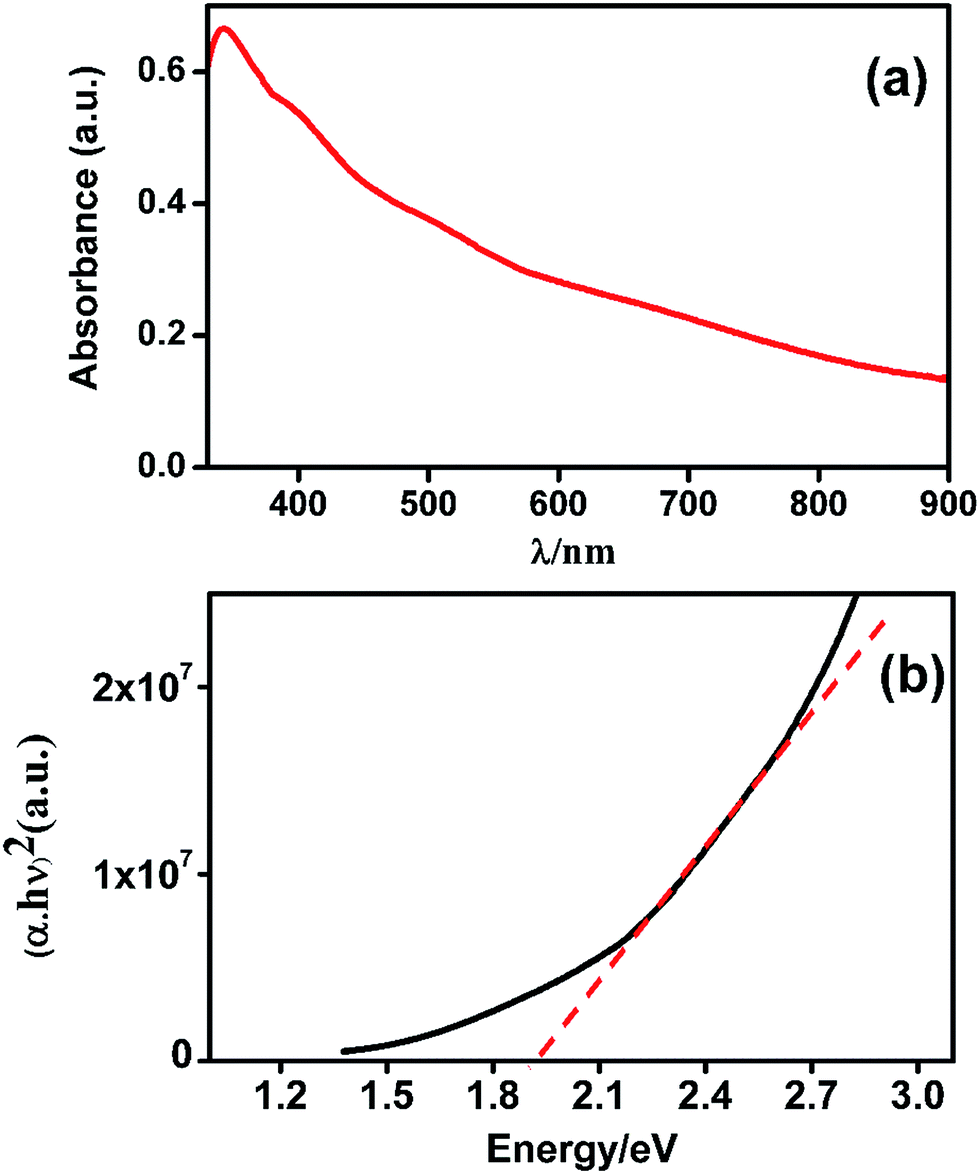
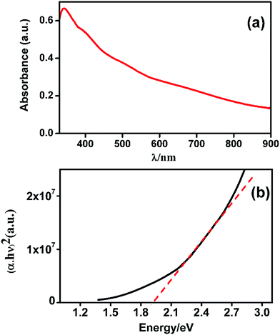
The UV-Vis spectra of the composite CuO–MnO–2TiO2 thin film having thickness of 665 nm was recorded in the region of 330–900 nm is shown in Fig. 6a. It is apparent that the film shows wide range absorption which gradually increases towards lower wavelength and shows the maximum absorption in the range of 790–330 nm giving maximum absorption peak at 340 nm. The optical band gap of CuO–MnO–2TiO2 composite is determined by the Tauc's equation.45
where α is the linear absorption coefficient of the material, hν is the photon energy, A is a proportionality constant and γ is a constant depending on the band gap nature; γ = 1/2 for allowed direct band gap and γ = 2 for indirect band gap.
 |
| | Fig. 6 (a) UV-Vis spectra of absorbance as a function of wavelength and (b) Tauc's plot of energy vs. (αhν)2 of CuO–MnO–2TiO2 composite thin film deposited by AACVD at 550 °C. | |
The direct band gap was calculated by using Tauc's equation arranged as (αhν)2 = A1(hν − Eg). A plot of (αhν)2 versus hν in Fig. 6b gave a linear region with slope A1 whose extrapolation to α(hν) = 0 would yield the value of the direct band gap of 1.95 eV for thin film fabricated at 550 °C. The reported band gap is 1.2–1.5 eV for CuO,20,46 3.69 eV for MnO,47 3.2–3.4 eV for pure anatase phase of TiO2 (ref. 19 and 48) and 3.0 eV for rutile phase of TiO2.49 However we found band gap edge at 1.95 eV for CuO–MnO–2TiO2 composite thin film. Band gap value is changed due to combination of individual wide and narrow band gap semiconductor, for controlling photocatalyst band structure.50 It is most probable that due to synergic effect of three components in the composite, the Fermi level equilibrium between these three metal oxides would result in the retardation of recombination of photo-generated charge carriers. In the mixed semiconductor system, photo-induced charge separation is facilitated by hole trapping process. Thus, the separation of photo-induced e−–h+ pair in this CuO–MnO–2TiO2 mixed semiconductor system could be enhanced as compared to individual semiconducting oxide, which ultimately improves the photocatalytic performance in the visible region of the solar spectrum.
3.6. Photo-electrochemical studies
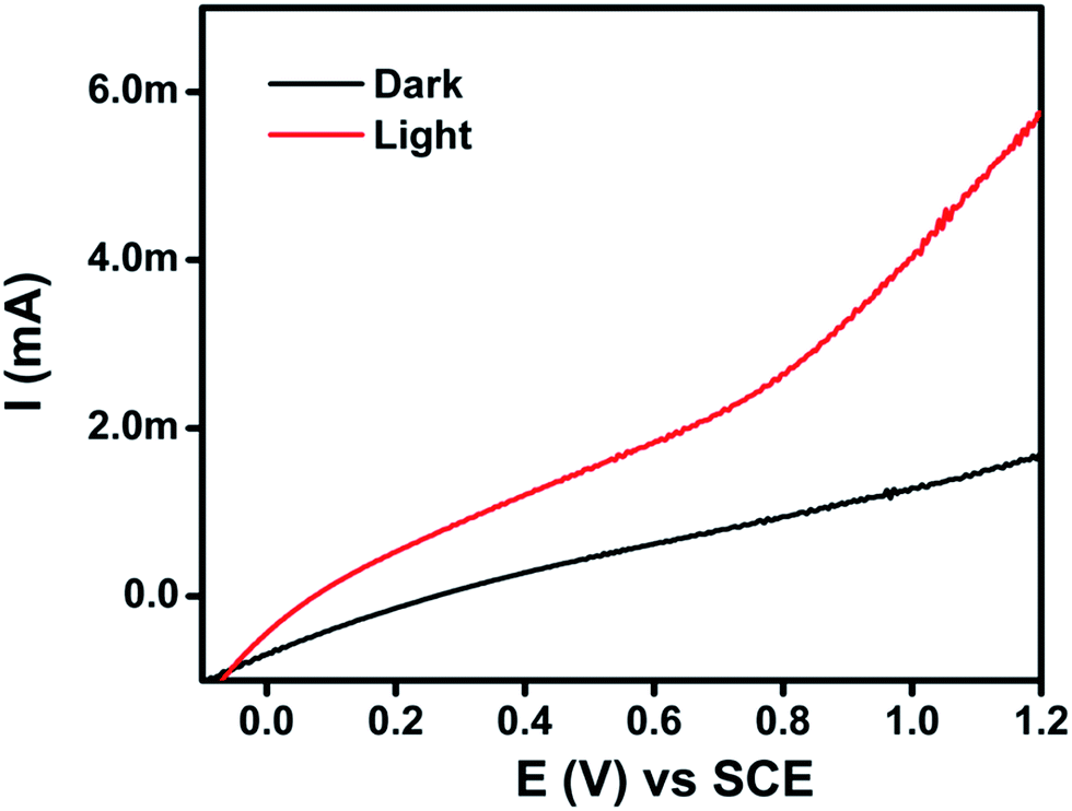
The as-synthesized CuO–MnO–2TiO2 thin film fabricated by the AACVD method was examined of its photoelectrochemical water splitting properties using linear scan voltammetry (LSV) technique, in 0.5 M Na2SO4 at a scan rate of 50 mV s−1 under dark and simulated solar irradiation of AM 1.5 G (100 mW cm−2), and is shown in Fig. 7. It can be seen that the CuO–MnO–2TiO2 thin film electrode produce photocurrent density of 2.21 mA cm−2 under sunlight illumination at bias potential of +0.7 V. The I–V plot presented in Fig. 7 shows that photoactivity commences at slightly negative potential with respect to the Ag/AgCl reference electrode. As the potential increases to the positive region, a steady increase in photocurrent occurs indicating the n-type nature of thin film and photoanodic behavior against counter electrode. Different factors such as crystal defects, threading dislocations are well reported that leads to an unusual increase in the dark current. These factors are prominent when matrix is composed of more than one components or if some dopant is added that results in lattice mismatch and crystal defects and eventually surface leakage of current is significant.51 We assume that in our trimetallic composite oxide matrix some dislocations are aroused due to lattice mismatch that facilitates temporary storage of electric current and making it a pseudocapacitor that results in high dark current.
 |
| | Fig. 7 Current–voltage (I–V) plot obtained for the AACVD produced CuO–MnO–2TiO2 composite thin film dipped in 0.5 M Na2SO4 at a scan rate of 50 mV s−1 in the absence and presence of simulated AM 1.5 G illumination of 100 mW cm−2. | |
CuO is a narrow bandgap semiconductor, acts as photocathode in PEC system generating a cathodic photocurrent (150 μA cm−2 at −0.4 V) typical of its p-type behavior.20 MnO has been widely studied as cathodic material for lithium ion batteries52 but it is hard to find any literature regarding its PEC water splitting performance. As reported earlier, TiO2 due to its large band gap has low absorption in the visible region of the solar spectrum and only produces photocurrent density of few microamperes.53 A schematic diagram of the relative conduction band (CB) and valence band (VB) positions54 of CuO, MnO, TiO2 are shown in Fig. 8a. CuO and MnO are p-type and TiO2 is n-type semiconducting material. The coupling of wider band gap and smaller band gap semiconductors could extend the visible light absorption, improve the charge separation and increase the life time of charge carriers by the photo-induced generated p–n junction interface.19 The electron transfer process between the mixed semiconductors could facilitate the charge separation mechanism through the formation of an internal electric field at the heterojunction interface, and thereby suppresses the of e−–h+ recombination under visible light irradiation.55 As displayed in Fig. 8b, upon light irradiation, an equilibrium state is formed between the CB and VB positions of CuO, MnO and TiO2 by raising the energy band of CuO and reducing the Fermi level of MnO and TiO2. The resulting inner electric field can efficiently drive the photo-generated electrons and holes to the CB of TiO2, MnO and VB of TiO2, CuO, respectively, thus decreasing the recombination of e−–h+ pairs and accelerating the photocatalytic reactions. The hole trapping process and efficient charge transfer is facilitated in the mixed semiconductor system which decreases the e−–h+ recombination. The enhanced PEC performance in CuO–MnO–2TiO2 is attributed to the synergistic effect in the mixed n and p type metal oxide system which increase the photogeneration efficiency.
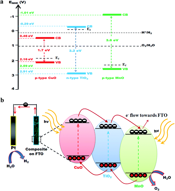 |
| | Fig. 8 (a) Schematic representation of energy band structure of p-type CuO, n-type TiO2 and p-type MnO before composite formation. (b) Schematic representation of the proposed realignment of energy bands after CuO–MnO–2TiO2 composite formation and PEC water splitting. | |
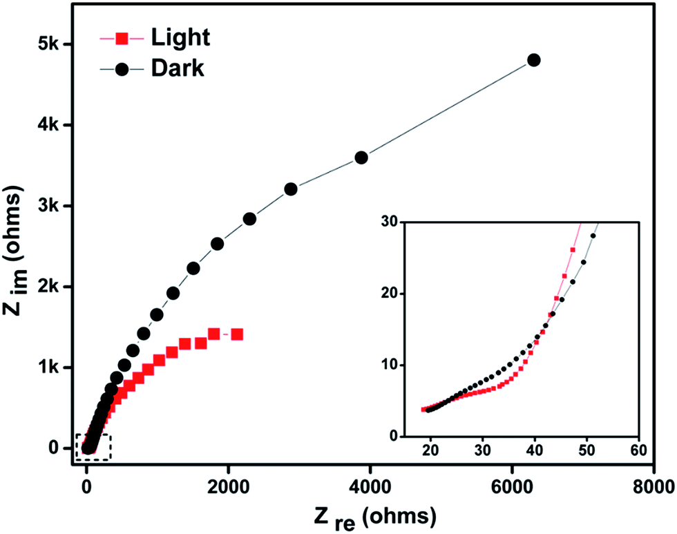
Electrochemical impedance spectroscopy (EIS) was performed to study the conductivity of electrode material, charge transport in the electrode–electrolyte interface and mechanistic analysis of interfacial processes. The Nyquist plot obtained from the EIS measurements under light and dark conditions for the CuO–MnO–2TiO2 thin film deposited at 550 °C in the presence of 0.5 M Na2SO4 in the frequency range of 0.1 Hz to 10 kHz is displayed in Fig. 9. The diameter of the semicircle in the Nyquist plot extending towards lower frequencies represents the charge transfer resistance (Rct), which is associated with the electronic properties of the electrode. The Rct value of CuO–MnO–2TiO2 thin film decreases significantly from 52.77 Ω to 32.08 Ω upon illumination, indicating an increase in the charge carriers due to low interfacial charge transfer resistance and decreasing the possibility of the charge recombination, thus enhancing the photocurrent response against water oxidation.
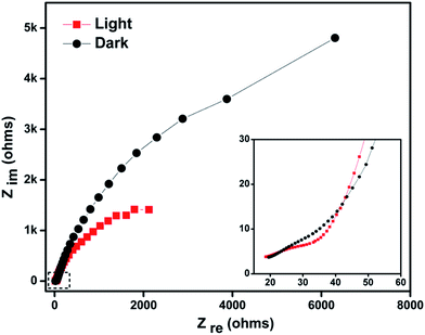 |
| | Fig. 9 Nyquist phase plot obtained for the CuO–MnO–2TiO2 thin film in the presence of 0.5 M Na2SO4 at frequencies ranges of 0.1 Hz to 10 kHz under and without light illumination. Inset: Nyquist plot at lower frequency range. | |
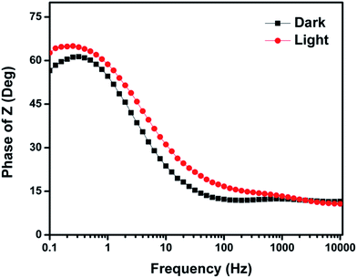
The frequency dependence and phase angle plot (Bode plot) of CuO–MnO–2TiO2 thin film was recorded for the detailed understanding of the charge-transfer resistance phenomenon in the composite. The Bode phase plot obtained for the CuO–MnO–2TiO2 thin film is shown in Fig. 10, where the characteristic frequency peak is affected in the dark and under illuminated conditions. The fmax is observed to shift towards the low frequency region in the presence of illumination, indicating a rapid electron-transfer (conductive) behavior of the CuO–MnO–2TiO2 thin film as compared in the dark. The fmax is related to the electron recombination lifetime (τn) of the corresponding material using from the following relationship.56
where
fmax is the frequency peak maximum. The Bode plot in
Fig. 10 shows that the
fmax shifts towards lower frequency (longer
τn) under illumination compared in the dark.
 |
| | Fig. 10 Bode angle phase plot of the CuO–MnO–2TiO2 thin film in the presence of 0.5 M Na2SO4 at frequencies ranges of 0.1 Hz to 10 kHz under and without light illumination. | |
As a result of longer τn due to decrease in the fmax, larger current density for the CuO–MnO–2TiO2 was observed thin film under illumination, which indicate that electrons survive from the recombination process, as also characterized by a smaller Rct in the Nyquist plot. The contribution of the different types of metal oxides in a mixed semiconducting system and band gap engineering resulted in the decrease in the recombination life time and thus significantly influence the PEC performance. The Bode plot in Fig. 10 also shows larger phase angle θ degrees under illumination compared in the dark. The increase in the phase angle is due to the larger capacitative behavior from the increase of charge accumulation, as a result from an increased photo-excitation process and decreased recombination process.
4. Conclusions
Thin films of trimetallic composite oxide, CuO–MnO–2TiO2, can be grown on FTO coated glass substrate by AACVD utilizing a homogeneous mixture of acetates of Cu and Mn and (Ti(O(CH2)3CH3)4) in the presence of trifluoroacetic acid in THF. The formation of the composite not only lowers the band gap energy of TiO2 but also reduces the possibility of e−–h+ recombination to enhance photoelectrochemical water splitting. A band gap of 1.95 eV and a maximum photocurrent density of 2.21 mA cm−2 at +0.7 V vs. Ag/AgCl/3 M KCl has been obtained for photoelectrode grown from THF solution at 550 °C for 45 minutes.
Acknowledgements
All the authors gratefully acknowledge the University of Malaya for its generous financial support through FRGS Grant No. FP039-2016, IPPP Grant No. PG053-2016A and UMRG Grant No. UM.TNC2/RC/261/1/1/RP007-13AET.
Notes and references
- A. A. Dubale, C. Pan, A. G. Tamirat, H. Chen, W. Su, C. Chen, J. Rick, D. W. Ayele, B. A. Aragaw, J. Lee, Y. Yang and B. Hwang, J. Mater. Chem. A, 2015, 3, 12482–12499 CAS.
- J. Han, X. Zong, X. Zhou and C. Li, RSC Adv., 2015, 5, 10790–10794 RSC.
- M. A. Mansoor, M. Mazhar, V. Mckee and Z. Arifin, Polyhedron, 2014, 75, 135–140 CrossRef CAS.
- M. A. Mansoor, M. Mazhar, M. Ebadi, H. N. Ming, M. A. M. Teridi and L. K. Mun, New J. Chem., 2016, 40, 5177–5184 RSC.
- M. A. Mansoor, M. Mazhar, A. Pandikumar, H. Khaledi, H. N. Ming and Z. Arifin, Int. J. Hydrogen Energy, 2016, 41, 9267–9275 CrossRef CAS.
- A. Fujishima and K. Honda, Nature, 1972, 238, 37–38 CrossRef CAS PubMed.
- M. A. Mansoor, N. M. Huang, V. Mckee, T. A. N. Peiris, K. G. U. Wijayantha, Z. Arifin, M. Misran and M. Mazhar, Sol. Energy Mater. Sol. Cells, 2015, 137, 258–264 CrossRef CAS.
- T. Miwa, S. Kaneco, H. Katsumata, T. Suzuki, K. Ohta, S. C. Verma and K. Sugihara, Int. J. Hydrogen Energy, 2010, 35, 6554–6560 CrossRef CAS.
- M. A. Subhan, N. Uddin, P. Sarker, A. K. Azad and K. Begum, Spectrochim. Acta, Part A, 2015, 149, 839–850 CrossRef CAS PubMed.
- M. A. Subhan, T. Ahmad, P. Sarker, T. T. Pakkanen, M. Suvanto, M. Horimoto and H. Nakata, J. Lumin., 2014, 148, 98–102 CrossRef CAS.
- C. Wang, B. Xu, X. Wang and J. Zhao, J. Solid State Chem., 2005, 178, 3500–3506 CrossRef CAS.
- Y. Lu, Y. Lin, T. Xie, S. Shi, H. Fan and D. Wang, Nanoscale, 2012, 4, 6393–6400 RSC.
- S. S. Shinde, C. H. Bhosale and K. Y. Rajpure, Catal. Rev., 2013, 55, 79–133 CAS.
- R. C. Smith, T. Ma, N. Hoilien, L. Y. Tsung, M. J. Bevan, L. Colombo, J. Roberts, S. A. Campbell and W. L. Gladfelter, Adv. Mater. Opt. Electron., 2000, 10, 105–114 CrossRef CAS.
- M. Ritala, K. Kukli, A. Rahtu, P. I. Raisanen, M. Leskela, T. Sajavaara and J. Keinonen, Science, 2000, 288, 319–321 CrossRef CAS PubMed.
- K. Zakrzewska, Thin Solid Films, 2001, 391, 229–238 CrossRef CAS.
- E. Comini, C. Baratto, G. Faglia, M. Ferroni, A. Vomiero and G. Sberveglieri, Prog. Mater. Sci., 2009, 54, 1–67 CrossRef CAS.
- F. E. Kruis, H. Fissan and A. Peled, J. Aerosol Sci., 1998, 29, 511–535 CrossRef CAS.
- J. Wen, X. Li, W. Liu, Y. Fang, J. Xie and Y. Xu, Chin. J. Catal., 2015, 36, 2049–2070 CrossRef CAS.
- R. Patil, S. Kelkar, R. Naphade and S. Ogale, J. Mater. Chem. A, 2014, 2, 3661–3668 CAS.
- H. Wang, X. Zhang, A. Huang, H. Xu, M. Zhu, B. Wang, H. Yan and M. Yoshimura, J. Cryst. Growth, 2002, 246, 150–154 CrossRef CAS.
- F. Vera, R. Schrebler, E. Muñoz, C. Suarez, P. Cury, H. Gómez, R. Córdova, R. E. Marotti and E. A. Dalchiele, Thin Solid Films, 2005, 490, 182–188 CrossRef CAS.
- T. Minami, H. Nanto and S. Takata, Jpn. J. Appl. Phys., 1984, 23, 280–282 CrossRef CAS.
- S. Madeswaran, N. V. Giridharan and R. Jayavel, Mater. Chem. Phys., 2003, 80, 23–28 CrossRef CAS.
- L. Jinlong, L. Tongxiang and W. Chen, J. Solid State Chem., 2016, 240, 109–114 CrossRef.
- L. R. de León-Gutiérrez, J. J. Cayente-Romero, J. M. Peza-Tapia, E. Barrera-Calva, J. C. Martínez-Flores and M. Ortega-López, Mater. Lett., 2006, 60, 3866–3870 CrossRef.
- N. Chaoui, E. Millon, J. F. Muller, P. Ecker, W. Bieck and H. N. Migeon, Mater. Chem. Phys., 1999, 59, 114–119 CrossRef CAS.
- P. Marchand, I. A. Hassan, I. P. Parkin, C. J. Carmalt and P. Marchand, Dalton Trans., 2013, 42, 9406–9422 RSC.
- A. A. Tahir, K. C. Molloy, M. Mazhar, G. Kociok-Köhn, M. Hamid and S. Dastgir, Inorg. Chem., 2005, 44, 9207–9212 CrossRef CAS PubMed.
- K. Borgohain, Phys. Rev. B: Condens. Matter Mater. Phys., 2000, 61, 93–96 CrossRef.
- K. J. Arun, A. K. Batra, A. Krishna, K. Bhat, M. D. Aggarwal and P. J. J. Francis, Am. J. Mater. Sci., 2015, 5, 36–38 Search PubMed.
- A. S. Ethiraj and D. J. Kang, Nanoscale Res. Lett., 2012, 7, 70 CrossRef PubMed.
- S. Mallakpour, M. Dinari and E. Azadi, Int. J. Polym. Anal. Charact., 2015, 20, 82–97 CrossRef CAS.
- M. Zheng, H. Zhang, X. Gong, R. Xu, Y. Xiao, H. Dong, X. Liu and Y. Liu, Nanoscale Res. Lett., 2013, 8, 166 CrossRef PubMed.
- M. Khan, A. H. Naqvi and M. Ahmad, Toxicol. Rep., 2016, 2, 765–774 CrossRef.
- M. A. Ehsan, R. Naeem, V. McKee, A. H. Saeed, A. Pandikumar, N. M. Huang and M. Mazhar, RSC Adv., 2016, 6, 27852–27861 RSC.
- T. H. Nguyen, T. L. Nguyen, T. D. T. Ung and Q. L. Nguyen, Adv. Nat. Sci.: Nanosci. Nanotechnol., 2013, 4, 25002 CrossRef.
- K. Ramesh, L. Chen, F. Chen, Y. Liu, Z. Wang and Y. F. Han, Catal. Today, 2008, 131, 477–482 CrossRef CAS.
- M. A. Mansoor, M. Ebadi, M. Mazhar, N. M. Huang, L. K. Mun, M. Misran and W. J. Basirun, Mater. Chem. Phys., 2017, 186, 286–294 CrossRef CAS.
- M. A. Dar, S. H. Nam, Y. S. Kim and W. B. Kim, J. Solid State Electrochem., 2010, 14, 1719–1726 CrossRef CAS.
- J. Huang, S. Wang, Y. Zhao, X. Wang, S. Wang, S. Wu, S. Zhang and W. Huang, Catal. Commun., 2006, 7, 1029–1034 CrossRef CAS.
- L. Zhu, M. Hong and G. W. Ho, Nano Energy, 2015, 11, 28–37 CrossRef CAS.
- S. Ma, D. Chen and W. Wang, Phys. Chem. Chem. Phys., 2016, 18, 19130–19136 RSC.
- M. C. Biesinger, B. P. Payne, A. P. Grosvenor, L. W. M. Lau, A. R. Gerson and R. S. C. Smart, Appl. Surf. Sci., 2011, 257, 2717–2730 CrossRef CAS.
- F. Yakuphanoglu, S. Ilican, M. Caglar and Y. Caglar, J. Optoelectron. Adv. Mater., 2007, 9, 2180–2185 CAS.
- D. Chauhan, V. R. Satsangi, S. Dass and S. Rohit, Bull. Mater. Sci., 2006, 29, 709–716 CAS.
- J. V. Elp, R. H. Potze, H. Eskes, R. Berger and G. A. Sawatzky, Phys. Rev. B: Condens. Matter Mater. Phys., 1991, 44, 1530–1537 CrossRef.
- K. M. Reddy, S. V. Manorama and A. R. Reddy, Mater. Chem. Phys., 2003, 78, 239–245 CrossRef.
- A. Kudo and Y. Miseki, Chem. Soc. Rev., 2009, 38, 253–278 RSC.
- X. Chen, S. Shen, L. Guo and S. S. Mao, Chem. Rev., 2010, 110, 6503–6570 CrossRef CAS PubMed.
- M. Takenaka, K. Morii, M. Sugiyama, Y. Nakano and S. Takagi, Opt. Express, 2012, 20, 8718–8725 CrossRef CAS PubMed.
- K. Zhong, X. Xia, B. Zhang, H. Li, Z. Wang and L. Chen, J. Power Sources, 2010, 195, 3300–3308 CrossRef CAS.
- X. Shi, K. Ueno, T. Oshikiri and H. Misawa, J. Phys. Chem. C, 2013, 117, 24733–24739 CAS.
- Y. Xu and M. A. A. Schoonen, Am. Mineral., 2000, 85, 543–556 CrossRef CAS.
- A. G. Tamirat, J. Rick, A. A. Dubale, W. N. Su and B. J. Hwang, Nanoscale Horiz., 2016, 1, 243–267 RSC.
- S. P. Lim, A. Pandikumar, N. M. Huang, H. N. Lim, G. C. Gu and T. L. Ma, RSC Adv., 2014, 4, 48236–48244 RSC.
Footnote |
| † Electronic supplementary information (ESI) available. See DOI: 10.1039/c6ra28752b |
|
| This journal is © The Royal Society of Chemistry 2017 |
Click here to see how this site uses Cookies. View our privacy policy here. 
 Open Access Article
 This Open Access Article is licensed under a
  b and
Muhammad Mazhar
b and
Muhammad Mazhar ) at 2θ = 27.43 (110), 36.07 (011), 39.18 (020), 54.31 (121), 65.50 (221), 68.99 (031) are attributed to tetragonal rutile TiO2. The rest of reflections are assigned to FTO substrate (ICDD card no. [00-007-0195]). Sticky pattern matching is available in (Fig. S1†).