
 Open Access Article
 This Open Access Article is licensed under a Creative Commons Attribution-Non Commercial 3.0 Unported Licence
Unravelling the energy transfer mechanism in bismuth co-activation of LaInO3:Sm3+/Ho3+ nanophosphor for color-tunable luminescence†
Ch. Satya Kamalac,
T. K. Visweswara Raoac,
P. V. S. S. S. N. Reddya,
K. Sujathaa,
Babajide Patrick Ajayib,
Jacek B. Jasinskib and
K. Ramachandra Rao *ab
*ab
aCrystal Growth and Nano-Science Research Center, Department of Physics, Government College (A), Rajamahendravaram, Andhra Pradesh, India-533105. E-mail: drkrcr@gmail.com
bConn Center for Renewable Energy Research, University of Louisville, KY, USA
cDepartment of Physics, Adikavi Nannaya University, Rajamahendravaram, Andhra Pradesh, India
First published on 2nd February 2017
Abstract
A series of single-phased and color tunable LaInO3:Bi3+,Ho3+/Sm3+ nano phosphors were synthesized via a cost effective and low temperature chemical route. The crystal structure, morphology, photoluminescence (PL) and energy transfer mechanism between Bi3+ to Ho3+/Sm3+ were investigated in detail. The considerable spectral overlap between the broad emission band of Bi3+ around 400–500 nm and the excitation band of Ho3+ and Sm3+ supports the efficient energy transfer from Bi3+ to Ho3+/Sm3+, which enhances the PL intensity remarkably. The energy transfer efficiency between Bi3+ and Ho3+/Sm3+ in LaInO3 was also calculated and the efficiency increased linearly with increasing concentration of Ho3+ and Sm3+. The emission hue can be tuned from blue to green and pink by varying the content of Ho3+/Sm3+. This investigation will extend an understanding of interactions between Bi3+ and rare earth ions in semiconducting host LaInO3 and show the potential applications of Bi3+, Ho3+/Sm3+ co-doped nanophosphors in displays and light emitting diodes.
Introduction
Owing to the gradual increase in energy consumption, light emitting diodes, as fourth generation lighting source, have been used widely in general illumination purposes and for display applications on account of their excellent characteristics. The manufacture of LEDs using inorganic phosphors or single-phase emitting phosphors excited by ultraviolet (UV) chips has received great attention. The single-phase phosphor-converted UV LEDs and phosphors with excellent red and green emission properties have become a vital part in the field of back lighting display applications. In the view of the abovementioned reasons, research on rare earth (RE) activated luminescence materials plays a major technological role in lighting applications. Indeed, the absorption cross section of RE ions is small because of the parity forbidden character of 4f–4f transitions, and consequently RE ions cannot be excited directly by illuminating light.1–8 Therefore, to improve the efficiencies and luminescence properties of RE ions, several methods are chosen, such as host absorption, f–d absorption, charge transfer state absorption, and energy transfer (ET).Rare earth (RE) and transition ion-doped aluminates and gallates have been studied extensively for their display applications.9–14 SrAl2O4:Dy3+,Eu2+ has been regarded to deliver a good green long persisting phosphorescence.15 Furthermore, indates, being used as the host lattice for luminescence and being doped with rare-earth ions were also reported.15–19 A few rare-earth doped LaInO3 phosphors have been reported as an alternative luminescence material because of their high thermal and chemical stability. Silicon coated core–shell structured LaInO3:Sm3+,Tb3+ phosphors have been used for their diverse luminescent properties.20–23 Despite their use as a photoluminescent host, the energy transfer mechanism between sensitizer and activator is still unclear.
The semiconducting compound, LaInO3, with a bandgap of 3.2 eV, belongs to the orthorhombically distorted perovskite-like structure with the space group Pnma24 and is found to be a potential candidate for several applications in various fields, such as oxygen sensing,25 solid oxide fuel cells (SOFC) and the presence of In3+ in the host lattice enhances its electrical conductivity, which can be used for display applications.26 Semiconducting oxide-based phosphors like LaInO3 are promising candidates with sufficient conductivity to overcome the charge build-up on the phosphor surfaces, in addition to their thermal and chemical stability.27,28 L. I. van Steensel et al. showed that LaInO3:Bi3+ is an efficient, blue-emitting photo luminescent material29 and researchers have reported that on co-doping with Bi3+, it acts as an excellent sensitizer to enhance the luminescence of RE ions in a wide variety of hosts.30–38 The emission spectrum of Bi3+ contains a broad band, whose peak maximum varies from blue to green for different host lattices39 because the outer 6s2 electronic configurations of Bi3+ depend strongly on their environmental conditions, such as covalence, coordination number and site symmetry.40–42 Among the RE ions, Sm3+ and Ho3+ are important activators for producing significant orange-red and green emissions for wide applications in optical displays, remote sensing and medical purposes.43,44 However, it is quite a challenge to select a proper host because doping and co-doping influence the optical properties of luminescence materials.
In this study, LaInO3, a semiconducting luminescent material was used as the host material. To the best of our knowledge, no accurate information is available on Sm3+ or Ho3+-doped LaInO3 phosphor co-doped with Bi3+ ions. These phosphors were synthesized using the polyol route. The morphological structures, steady state conditions and decay times were investigated. Their luminescent properties as well as energy transfer (ET) process and efficiency (ηET) from Bi3+ to Ho3+/Sm3+in LaInO3:Bi3+,Sm3+ and Ho3+ phosphors were investigated systematically. Remarkably, the color tunability of LaInO3:Bi3+,Sm3+ and Ho3+ phosphors varied with the doping concentration of Sm3+ and Ho3+.
Experimental
Preparation of the nanoparticles
La(NO3)3·6H2O [Merck, Germany], In(NO3)3·H2O [Alfa Aesar 99.99%], Bi(NO3)·5H2O [BDH Laboratory Chemicals Division, India], Sm(NO3)3·5H2O [Alfa Aesar 99.99%] and Ho(NO3)3·5H2O [Sigma-Aldrich 99.9%] were used as starting materials. Herein, ethylene glycol was used as the capping agent and urea was used for hydrolysis. For the preparation of pure LaInO3 nanoparticles, both La(NO3)3·6H2O and In(NO3)3·H2O were dissolved in the required amount of distilled water. To this solution, ethylene glycol (25 mL) was added and the mixture was then transferred into a two-necked RB flask. The solution was slowly heated up to 100 °C, followed by the addition of 2 g of urea, and the temperature was increased to 120 °C. At this temperature, the solution became turbid. The temperature was maintained at this value for 2 hours. The precipitate was collected after the reaction by centrifugation and then washed two times with acetone and three times with methanol, followed by drying under ambient conditions. The samples thus prepared were finally heated to 700 °C, 900 °C and 1000 °C in air at a heating rate of 10 °C per minute. The temperature was maintained at the respective values for a duration of 5 hours. Subsequently, the furnace was switched off and the sample was subjected to natural cooling to room temperature. The same procedure was used to prepare LaInO3:(1, 3, and 5 at%)Bi3+, LaInO3:3at%Bi3+,(0.5, 1, 1.5 at%)Ho3+ and LaInO3:3at%Bi3+,(1, 1.5, 2, 2.5 at%)Sm3+ nanoparticles and were subjected to heating at 1000 °C in air at a heating rate of 10 °C per minute.Characterization
X-ray diffraction (XRD) was carried out using a Philips powder X-ray diffractometer (model PW 1071) with Ni filtered Cu-Kα radiation. For calibration purposes, the diffraction peak corresponding to the (111) plane of Si at a 2θ value of 28.442° was employed. The XRD data was processed using POWDERX software. The average crystallite size was calculated from the diffraction line width based on Scherrer equation D = 0.9λ/β![[thin space (1/6-em)]](https://www.rsc.org/images/entities/char_2009.gif) cosθ, where D is the average particle size, λ is the wavelength of X-rays and β is the corrected full width at half maximum (FWHM). All luminescence measurements were carried out at room temperature with a resolution of 5 nm using an Edinburgh Instruments FLSP 920 system attached with a 450 W Xe lamp as the excitation source. A micro second flash lamp and a nanosecond hydrogen flash lamp was used for the lifetime measurements. The SEM instrument used was from Seron Inc. (Model AIS 2100) having a standard tungsten filament. An accelerating voltage of 20 kV and magnification of 10k× was used to record the micrographs.
cosθ, where D is the average particle size, λ is the wavelength of X-rays and β is the corrected full width at half maximum (FWHM). All luminescence measurements were carried out at room temperature with a resolution of 5 nm using an Edinburgh Instruments FLSP 920 system attached with a 450 W Xe lamp as the excitation source. A micro second flash lamp and a nanosecond hydrogen flash lamp was used for the lifetime measurements. The SEM instrument used was from Seron Inc. (Model AIS 2100) having a standard tungsten filament. An accelerating voltage of 20 kV and magnification of 10k× was used to record the micrographs.
Results & discussion
XRD analysis
Fig. 1 shows the XRD patterns of LaInO3:Bi3+(3 at%), LaInO3:(3 at%)Bi3+,(1 at%)Ho3+, and LaInO3:(3 at%)Bi3+,(2 at%)Sm3+ phosphors. The crystallinity, crystallite size and surface morphology have significant effects on the PL properties of phosphor materials. The XRD patterns of pure LaInO3 calcined at three different temperatures (700 °C, 900 °C, 1000 °C) is shown in ESI Fig. 1a,† indicating that LaInO3 began to crystallize at 700 °C. All the diffraction peaks of the doped and co-doped LaInO3 samples annealed at 1000 °C are in agreement with the previously reported data,26,45 indicating that the obtained samples are in a pure orthorhombic phase, where no impurity phase is detected, indicating that the dopants dissolved completely in the LaInO3 host lattice.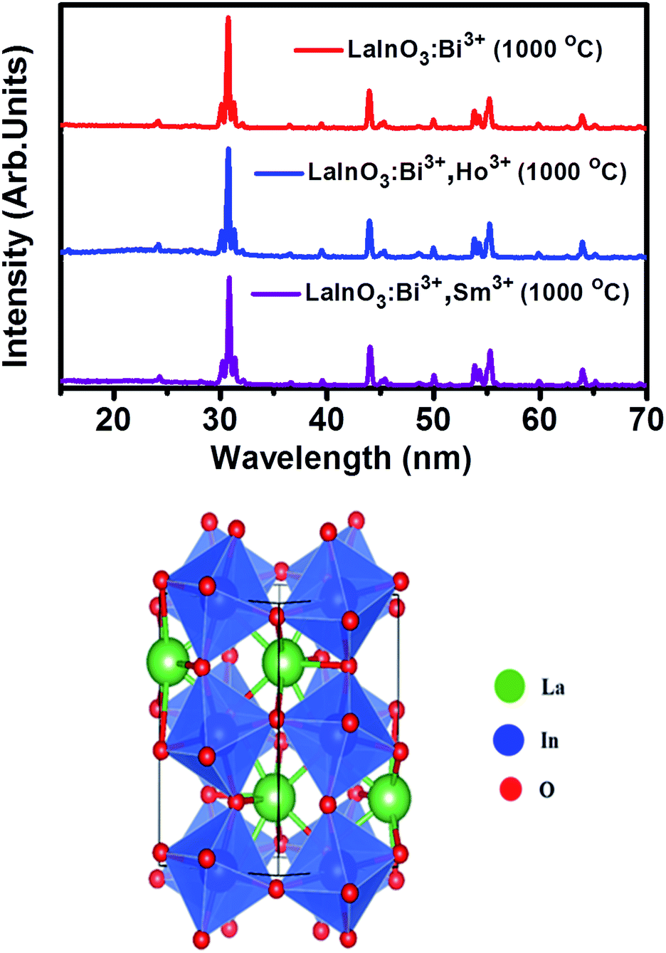 | ||
| Fig. 1 XRD patterns corresponding to LaInO3:Bi3+(3 at%), LaInO3:(3 at%)Bi3+,(1 at%)Ho3+, LaInO3:(3 at%)Bi3+,(2 at%)Sm3+ at 1000 °C and 3-D crystal structure of LaInO3. | ||
In addition, it can be observed from ESI Fig. 1b† that the diffraction peak positions are shifted slightly to a higher angle, when Bi3+ or Bi3+, Ho3+/Sm3+ ions were doped into the LaInO3 host, which can be due to the replacement of larger-size La3+ (1.16 Å) sites by the smaller-size trivalent Ho3+, Sm3+ and Bi3+ ions (1.051 Å, 1.08 Å, and 1.03 Å), leading to lattice distortion, consequently contracting the lattice parameters, as illustrated in ESI Table S1.† The three-dimensional structure diagram shows the crystal structure of LaInO3, the blue octahedrons represent the InO6 units, whereas La3+ is in the center of the eight InO6 octahedrons; hence, rare earth dopants Ho3+ or Sm3+ and Bi3+ will be replacing La3+ in the LaInO3 structure. The crystallite size of all the samples was calculated from the Scherrer equation D = 0.9λ/βcosθ, where D is the average particles size, λ is the wavelength of X-rays and β is the corrected full width at half maximum (FWHM) of an observed peak.46 The average crystallite size (D) of pure LaInO3, doped and co-doped LaInO3 particles, which are annealed at 1000 °C, were estimated to be around 35 nm.
SEM with energy dispersive X-ray analysis
Fig. 2a and b shows the Scanning Electron Microscopy (SEM) images of LaInO3:(3 at%)Bi3+,(1 at%)Ho3+, and LaInO3:(3 at%)Bi3+,(2 at%)Sm3+ samples. Crystallization granules and agglomeration of particles were observed in the present phosphors. ESI Fig. 2a and b† shows an SEM image of pure LaInO3, indicating irregular spherical particles with a size between 20 and 70 nm. This may be due to agglomeration among the phosphor particles during calcination. Compared to the Bi3+ single-doped sample, the Bi3+, Ho3+/Sm3+ co-doped phosphors have a smaller particle size distribution. Hence, the effect of coalescence could be decreased by single and co-doping in the host. The decrease in particle size is also explained as follows: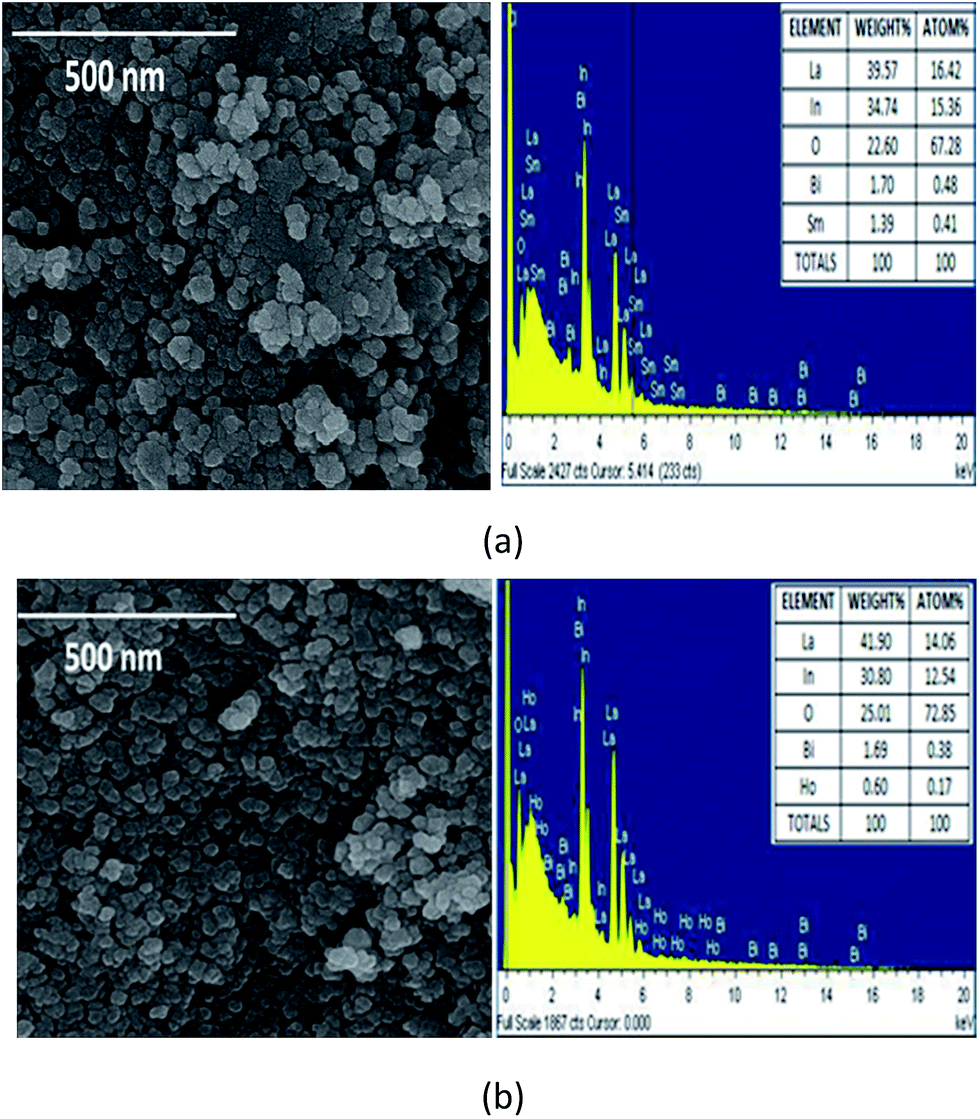 | ||
| Fig. 2 (a and b) SEM images and EDAX spectra's of (a) Bi3+, Ho3+ and (b) Bi3+, Sm3+ doped LaInO3. | ||
In poly synthesis, ethylene glycol acts as the capping agent for covering the nanoparticles and controlling the agglomeration. On the other hand, during annealing at 1000 °C, the ligand evaporates and nanoparticles due to high surface energy form a neck by solid state diffusion process, which leads to agglomeration and particle growth. The differences in ionic radii between La3+ and Bi3+, Ho3+, and Sm3+ ions lead to a lattice distortion, which encourages a decrease in particle size. Hence, crystallite and particle size reduces by co-doping due to a grain growth inhibition effect. Energy dispersive X-ray spectroscopy (EDS) was used to determine the composition of the samples and it shows good agreement with the nominal sample composition. (Refer to the inset of Fig. 3a and b.)
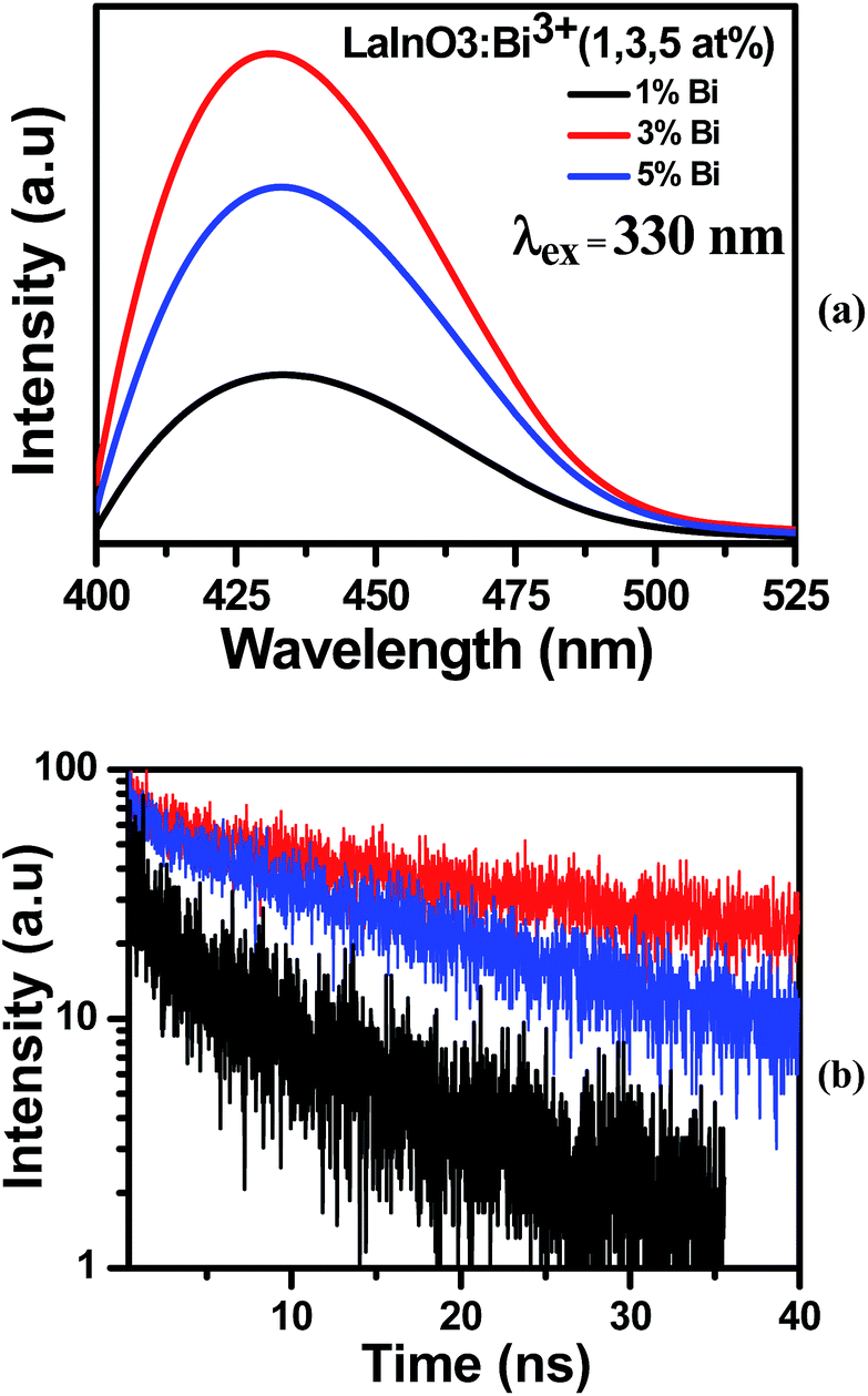 | ||
| Fig. 3 (a and b) Emission and decay curves of the LaInO3:Bi3+(1, 3, 5 at%) samples heat at 1000 °C. | ||
Photoluminescence and energy transfer mechanism
The emission and decay spectra of LaInO3:Bi3+(1, 3, and 5 at%) samples heated to 1000 °C are given in Fig. 3a and b respectively. From Fig. 3a, it can be observed that all samples have broad emission band centered at 432 nm, which can be attributed to the 3P1–1S0 transition of Bi3+ ions upon excitation with 330 nm.29 With increasing Bi3+ concentration, the intensity of the 432 nm emission band increases and reaches a maximum at 3 at% and then decreases remarkably when the Bi3+ content is increased further, which is due to concentration quenching. This is also confirmed by corresponding average bi-exponential life time value (295, 329, 273 ns) of decay curves shown in Fig. 3(b). In the excitation spectra (ESI Fig. 3†), a broad excitation band ranging from 300 to 350 nm with a maximum at about 330 nm was observed, arising from 1S0–3P1 transition of Bi3+.The overlap spectra of the emission and allowed absorption create interest on the effective radiative energy transfer (ET) mechanism. Fig. 4 presents the excitation spectra of LaInO3:Sm3+(2 at%) LaInO3:Ho3+(1 at%) and emission spectra of LaInO3:Bi3+(3 at%) samples. The appearance of the excitation bands of Ho3+ and Sm3+ was clearly visible in the emission bands of Bi3+. Therefore, it is expected that efficient energy transfer can occur from Bi3+ to Ho3+/Sm3+.
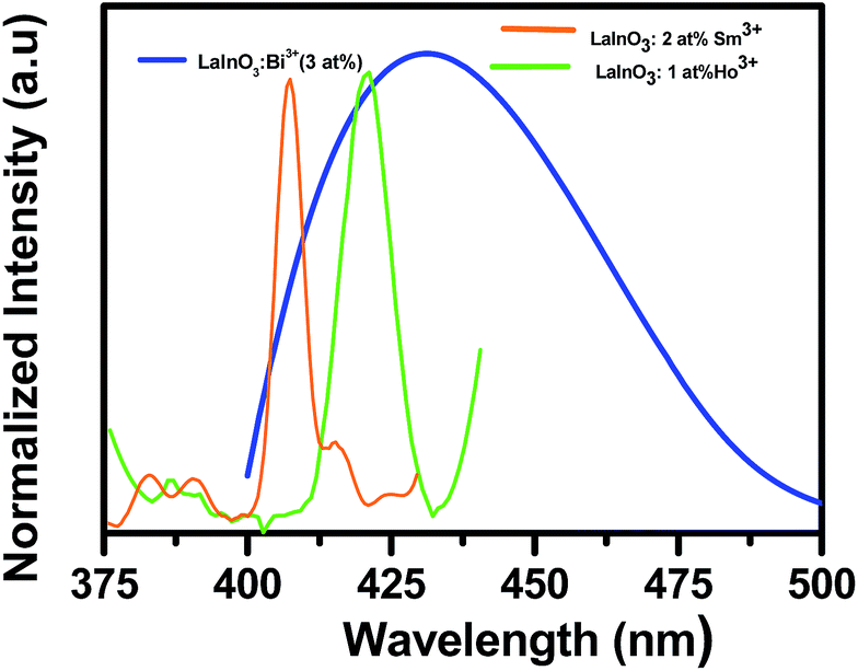 | ||
| Fig. 4 Spectral overlap of excitation spectra of LaInO3:Sm3+(2 at%), LaInO3:Ho3+(1 at%) and emission spectra of LaInO3:Bi3+(3 at%) samples heated at 1000 °C. | ||
The excitation spectra of the Bi3+, Ho3+/Sm3+-doped samples monitored at rare earth (RE) emission lines (544 nm and 603 nm) exhibited a broad excitation band arising from the 1S0–3P1 transition of Bi3+ in the wavelength range of 300–350 nm, accompanying the Ho3+/Sm3+ excitation lines. The same is shown in Fig. 5a–d, which represents the excitation and emission spectra of LaInO3:3at%Bi3+,(0.5, 1, 1.5 at%)Ho3+ and LaInO3:3at%Bi3+,(1, 1.5, 2, 2.5 at%)Sm3+ samples.
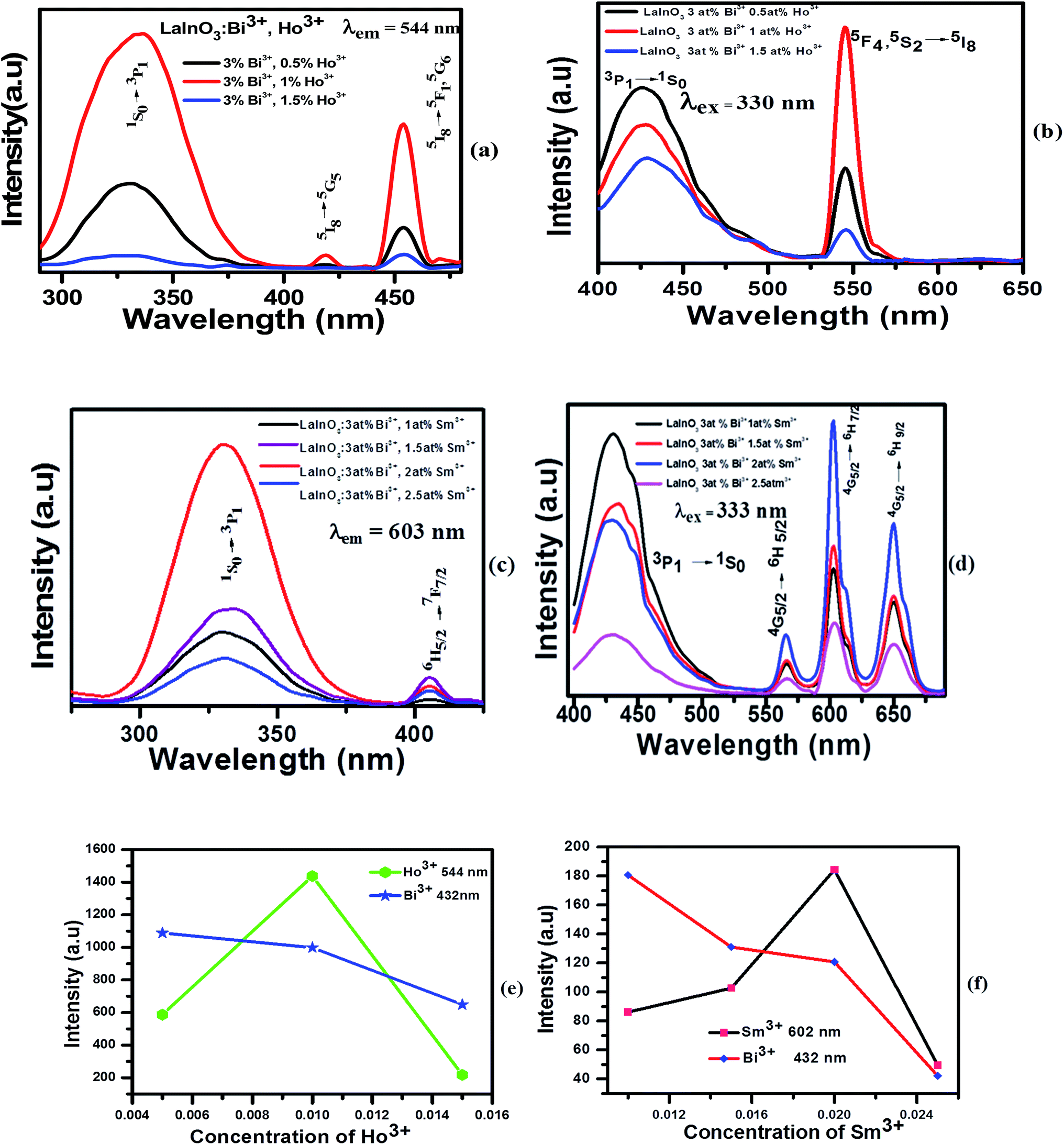 | ||
| Fig. 5 Excitation and emission spectra of LaInO3:3at%Bi3+,(0.5, 1, 1.5 at%)Ho3+ (a and b) and LaInO3:3at%Bi3+,(1, 1.5, 2, 2.5 at%)Sm3+ (c and d) heated at 1000 °C. Variations in the emission intensity for Sm3+/Ho3+ and Bi3+ with different (e) Sm3+/Ho3+ (f) concentrations. | ||
Under 330 nm and 333 nm excitation wavelengths, the samples consist of both blue-green emissions from Bi3+ and strong green emissions from Ho3+ and orange red emission from Sm3+. By keeping Bi3+ at 3 at% and varying the Ho3+ and Sm3+ content, the intensity of Bi3+ emission decreases monotonously, whereas the intensity of Ho3+/Sm3+ emission increases gradually and reaches a maximum at Ho3+ (1 at%) and Sm3+ (2 at%), and the Ho3+ and Sm3+ emissions then decrease with further increase in concentration, which can be rationalized as concentration quenching. The changes in emission intensity of Bi3+ as a function of Sm3+ and Ho3+ concentrations is clearly demonstrated in Fig. 5e–f. All abovementioned processes show that the emissions of Ho3+ and Sm3+ actually come from the ET process from Bi3+ to Ho3+/Sm3+ ions. To investigate the effect of Bi3+ doping in enhancing the PL intensity, single doped Ho3+/Sm3+:LaInO3 emission spectra are shown in ESI Fig. 4.† In addition, to support this ET process, the decay curves of all samples were measured, as shown in Fig. 6. For all samples, bi exponential luminescence decay curves were obtained and the lifetimes were characterized using the average lifetime (τ). The luminescence decay times (τ) of Bi3+ were obtained at 260, 228 and 192 ns for LaInO3:Bi3+(3 at%),Ho3+(0.5, 1, 1.5 at%) and for LaInO3:Bi3+(3 at%),Sm3+(1, 1.5, 2, 2.5 at%) 303, 291 and 211, 182 ns and also the corresponding decay times of Ho3+ 149, 179, and 122 μs, Sm3+ 1.22, 1.42, 1.73 and 1.13 ms, respectively. The increase in Ho3+/Sm3+ content leads to the faster decay of Bi3+ emission, which was attributed to ET from Bi3+ to Ho3+/Sm3+. The corresponding energy level diagram of LaInO3:Bi3+,Ho3+ and LaInO3:Bi3+,Sm3+ with optical transitions and energy transfer process are displayed in Fig. 7. In this process, when excited by UV energy, the electrons of Bi3+ ions absorb energy and jump from the ground state 1S0 to a higher level excited state 3P1; the excited electrons then relax to the lower energy level (the bottom of parabola) by non-radiative relaxation. Hence, from the lower energy level of 3P1, energy can be transferred to the 4K11/2 level of Sm3+ and 5F1 level of Ho3+ via an ET process (Cross relaxation) between these levels. Therefore, by co-doping with Bi3+ ions might improve the emission intensity of Sm3+ and Ho3+. Finally, a part of the electrons of Bi3+ ions may radiate back to the ground state by emitting blue emission and can be reabsorbed by the ground state levels of Sm3+ and Ho3+ i.e. 6H5/2 and 5I8, which also leads to energy transfer (because spectral overlap is observed in both Sm3+ and Ho3+), and can be subsequently excited to the respective high level excited state. The excited electrons relax to the 5F4, 5S2 level of Ho3+ and the 4G5/2 level of Sm3+ by non-radiative transition, and finally electrons return to the ground states of Ho3+ and Sm3+ ions by emitting green and pink lines, respectively.
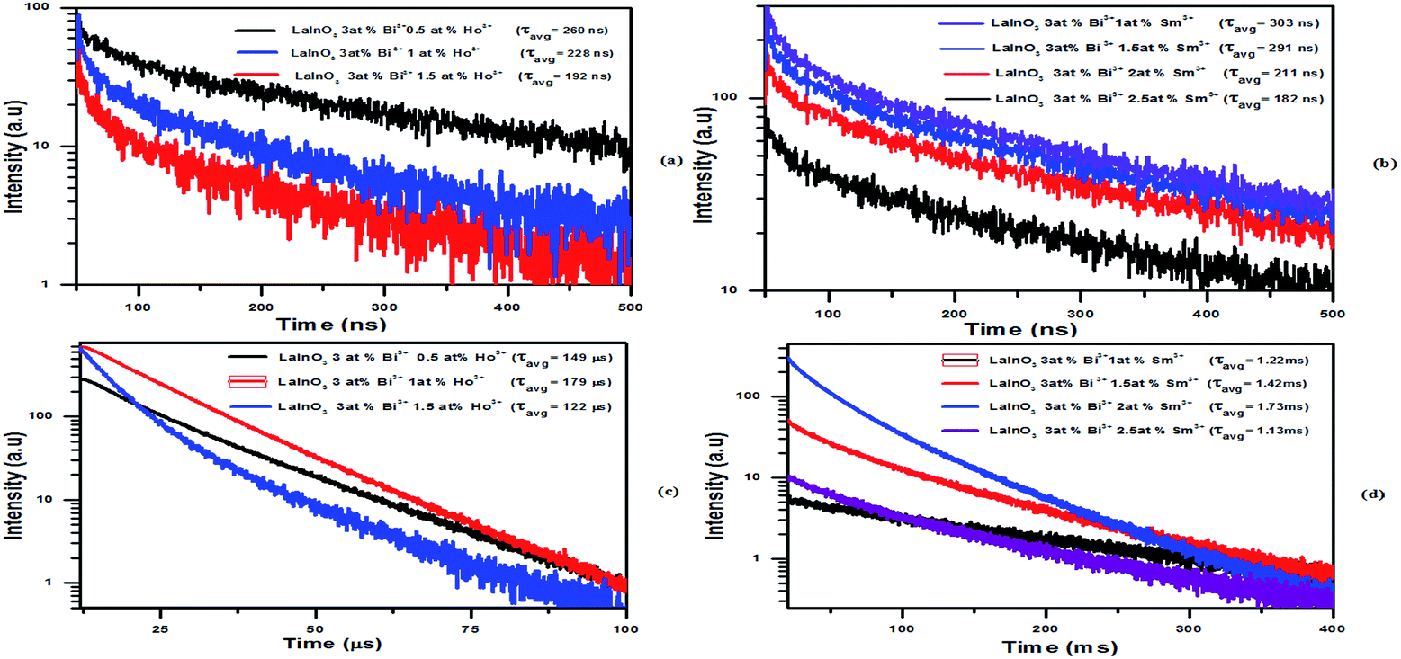 | ||
| Fig. 6 Decay curves of Bi3+ (a and b) and Ho3+, Sm3+ (c and d) in LaInO3:3at%Bi3+,(0.5, 1, 1.5 at%)Ho3+ and LaInO3:3at%Bi3+,(1, 1.5, 2, 2.5 at%)Sm3+. | ||
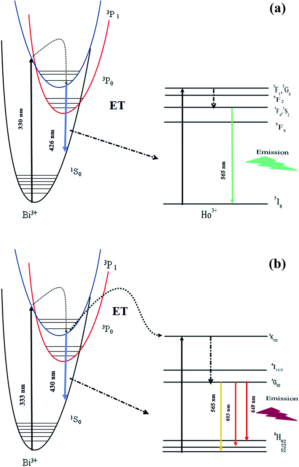 | ||
| Fig. 7 Energy level diagram and ET schemes of LaInO3:Bi3+,Ho3+ (a) Sm3+ (b). | ||
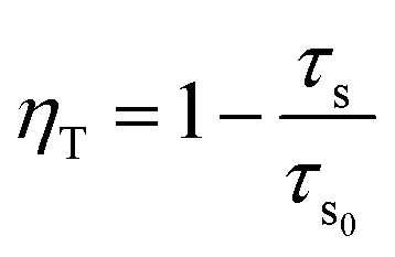
The ET efficiency ηT of Bi3+–Ho3+ and Bi3+–Sm3+ can be calculated using the following eqn (1)35,36
 | (1) |
| Phosphors | Concentration (x) | Efficiency ηET (%) |
|---|---|---|
| LaInO3:3at%Bi3+,xHo3+ | 0.5 | 39 |
| 1.0 | 42 | |
| 1.5 | 59 | |
| LaInO3:3at%Bi3+,xSm3+ | 1.0 | 0.8 |
| 1.5 | 12 | |
| 2.0 | 36 | |
| 2.5 | 45 |
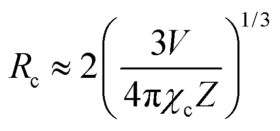
The critical distance Rc between Bi3+ and Ho3+/Sm3+ in the LaInO3 host can be estimated by the following equation:48
 | (2) |
To study the effect of the Ho3+/Sm3+ ions doping content on the color of LaInO3:3at%Bi3+, we synthesized a series of samples with the chemical compositions of LaInO3:3at%Bi3+,Ho3+(0.5, 1, 1.5 at%)/Sm3+(1, 1.5, 2, 2.5 at%). The Commission International de L'Eclairage (CIE) chromaticity coordinates of the single-phased emission-tunable phosphors are presented in Fig. 8. The CIE chromaticity coordinates of pure 3 at% Bi3+, 3 at% Bi3+, 1 at% Ho3+ and 3 at% Bi3+, 2 at% Sm3+ activated LaInO3 phosphors were (0.15, 0.03), (0.21, 0.25), and (0.33, 0.17) respectively. From the CIE diagram, it can be seen that the CIE chromaticity coordinates move from the bright blue to blue-green region and pink region as the amount of Ho3+/Sm3+ varies, indicating that the developed phosphor may potentially be used as a single phase phosphor for UV light-emitting diodes and field display applications.
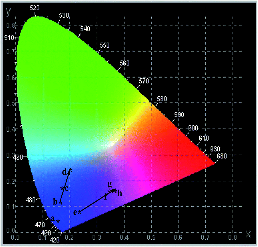 | ||
| Fig. 8 CIE chromaticity diagram of the (point a) LaInO3:3at%Bi3+, (points b–d) LaInO3:3at%Bi3+,(0.5, 1, 1.5 at%)Ho3+ and (points e–h) LaInO3:3at%Bi3+,(1, 1.5, 2, 2.5 at%)Sm3+ phosphors. | ||
Conclusion
We synthesized a series of single phased and color-tunable LaInO3:3at%Bi3+, LaInO3:3at%Bi3+,Ho3+(0.5, 1, 1.5 at%)/Sm3+(1, 1.5, 2, 2.5 at%) nanophosphors using the polyol method, and all the dopants were incorporated into the LaInO3 lattice, as determined via the XRD patterns. The photoluminescence properties, life time studies and energy transfer process were investigated in detail. The energy transfer from Bi3+ to Ho3+/Sm3+ and the energy transfer efficiency of LaInO3:3at%Bi3+,Ho3+ and LaInO3:3at%Bi3+,Sm3+ samples, which were calculated from the PL and decay curves, were 59 and 45%, respectively. Furthermore, the CIE diagram showed that the colors can be tuned from bright blue to blue-green and pink, indicating that the developed phosphor may potentially be used as a single phase phosphor for UV light-emitting diodes, VFD, FED, and other photoelectric fields.Acknowledgements
The authors are grateful to Dr V. Sudarsan, Scientist-G, Bhabha Atomic Research Centre (BARC) for PL studies and Dr R. David Kumar, Principal, Government College (A), Rajamahendravaram, Andhra Pradesh for necessary lab facilities.Notes and references
- G. Blasse and B. Grabmaier, Luminescent materials, Springer Science & Business Media, 2012 Search PubMed
.
- E. F. Schubert and J. K. Kim, Science, 2005, 308, 1274–1278 CrossRef CAS PubMed
- R. Wei, C. Ma, Y. Wei, J. Gao and H. Guo, Opt. Express, 2012, 20, 29743–29750 CrossRef CAS PubMed
- H. Guo, R. Wei and X. Liu, Opt. Lett., 2012, 37, 1670–1672 CrossRef CAS PubMed
- W.-R. Liu, C. C. Lin, Y.-C. Chiu, Y.-T. Yeh, S.-M. Jang and R.-S. Liu, Opt. Express, 2010, 18, 2946–2951 CrossRef CAS PubMed
- A. Kuznetsov, A. Nikitin, V. Tikhomirov, M. Shestakov and V. Moshchalkov, Appl. Phys. Lett., 2013, 102, 161916 CrossRef
- S. Nigam, C. S. Kamal, K. R. Rao, V. Sudarsan and R. K. Vatsa, J. Lumin., 2016, 178, 219–225 CrossRef CAS
- F. Wang, R. Deng, J. Wang, Q. Wang, Y. Han, H. Zhu, X. Chen and X. Liu, Nat. Mater., 2011, 10, 968–973 CrossRef CAS PubMed
- A. Baszczuk, M. Jasiorski, M. Nyk, J. Hanuza, M. Mączka and W. Stręk, J. Alloys Compd., 2005, 394, 88–92 CrossRef CAS
- Q. Shi, C. Wang, D. Zhang, S. Li, L. Zhang, W. Wang and J. Zhang, Thin Solid Films, 2012, 520, 6845–6849 CrossRef CAS
- C. S. Kamal, R. Mishra, D. K. Patel, K. R. Rao, V. Sudarsan and R. Vatsa, Mater. Res. Bull., 2016, 81, 127–133 CrossRef CAS
- M. Yu, J. Lin, Y. Zhou and S. Wang, Mater. Lett., 2002, 56, 1007–1013 CrossRef CAS
- X. Liu and J. Lin, J. Appl. Phys., 2006, 100, 124306 CrossRef
- T. Samuel, C. S. Kamal, K. Sujatha, V. Veeraiah, Y. Ramakrishana and K. R. Rao, Optik, 2016, 127, 10575–10587 CrossRef CAS
- X. Liu, R. Pang, Z. Quan, J. Yang and J. Lin, J. Electrochem. Soc., 2007, 154, J185–J189 CrossRef CAS
- X. Liu and J. Lin, J. Mater. Chem., 2008, 18, 221–228 RSC
- X. Liu, C. Lin and J. Lin, Appl. Phys. Lett., 2007, 90, 081904 CrossRef
- X. Liu, C. Li, Z. Quan, Z. Cheng and J. Lin, J. Phys. Chem. C, 2007, 111, 16601–16607 CAS
- X. Liu, C. Lin, Y. Luo and J. Lin, J. Electrochem. Soc., 2007, 154, J21–J27 CrossRef CAS
- S. K. Chaluvadi, V. Aswin, P. Kumar, P. Singh, D. Haranath, P. K. Rout and A. Dogra, J. Lumin., 2015, 166, 244–247 CrossRef CAS
- X. Liu, L. Yan and J. Lin, J. Electrochem. Soc., 2009, 156, P1–P6 CrossRef CAS
- X. Liu and J. Lin, Solid State Sci., 2009, 11, 2030–2036 CrossRef CAS
- Y. Shang, P. Yang, W. Wang, Y. Wang, N. Niu, S. Gai and J. Lin, J. Alloys Compd., 2011, 509, 837–844 CrossRef CAS
- D. Rogers, J. Honig and J. Goodenough, Mater. Res. Bull., 1967, 2, 223–230 CrossRef CAS
- V. Thangadurai and W. Weppner, J. Electrochem. Soc., 2001, 148, A1294–A1301 CrossRef CAS
- H. He, X. Huang and L. Chen, Solid State Ionics, 2000, 130, 183–193 CrossRef CAS
- H. He, X. Huang and L. Chen, Electrochim. Acta, 2001, 46, 2871–2877 CrossRef CAS
- K. Sood, K. Singh and O. Pandey, Trans. Indian Ceram. Soc., 2013, 72, 32–35 CrossRef CAS
- L. I. van Steensel, S. G. Bokhove, A. M. van de Craats, J. de Blank and G. Blasse, Mater. Res. Bull., 1995, 30, 1359–1362 CrossRef CAS
- F. Angiuli, E. Cavalli and A. Belletti, J. Solid State Chem., 2012, 192, 289–295 CrossRef CAS
- D. Chen, Y. Yu, P. Huang, H. Lin, Z. Shan, L. Zeng, A. Yang and Y. Wang, Phys. Chem. Chem. Phys., 2010, 12, 7775–7778 RSC
- Y. Zhydachevskii, L. Lipińska, M. Baran, M. Berkowski, A. Suchocki and A. Reszka, Mater. Chem. Phys., 2014, 143, 622–628 CrossRef CAS
- E. Cavalli, F. Angiuli, A. Belletti and P. Boutinaud, Opt. Mater., 2014, 36, 1642–1648 CrossRef CAS
- Z. Xia, D. Chen, M. Yang and T. Ying, J. Phys. Chem. Solids, 2010, 71, 175–180 CrossRef CAS
- L. Han, Y. Wang, J. Zhang and Y. Wang, Mater. Chem. Phys., 2013, 139, 87–91 CrossRef CAS
- L. Chen, K.-J. Chen, S.-F. Hu and R.-S. Liu, J. Mater. Chem., 2011, 21, 3677–3685 RSC
- X. Wei, Y. Chen, X. Cheng, M. Yin and W. Xu, Appl. Phys. B: Lasers Opt., 2010, 99, 763–768 CrossRef CAS
- H. Hara, S. Takeshita, T. Isobe, T. Sawayama and S. Niikura, Mater. Sci. Eng., B, 2013, 178, 311–315 CrossRef CAS
- P. Boutinaud, Inorg. Chem., 2013, 52, 6028–6038 CrossRef CAS PubMed
- L. Wang, Z. Lv, W. Kang, X. Shangguan, J. Shi and Z. Hao, Appl. Phys. Lett., 2013, 102, 151909 CrossRef
- L. Wang, Q. Sun, Q. Liu and J. Shi, J. Solid State Chem., 2012, 191, 142–146 CrossRef CAS
- H. Ju, W. Deng, B. Wang, J. Liu, X. Tao and S. Xu, J. Alloys Compd., 2012, 516, 153–156 CrossRef CAS
- Y. Zhang, Z. Zhu, W. Zhang and Y. Qiao, J. Alloys Compd., 2013, 566, 164–167 CrossRef CAS
- H. H. T. Vu, T. S. Atabaev, H.-K. Kim and Y.-H. Hwang, J. Nanosci. Nanotechnol., 2012, 12, 5847–5851 CrossRef CAS PubMed
- E. Ruiz-Trejo, G. Tavizon and A. Arroyo-Landeros, J. Phys. Chem. Solids, 2003, 64, 515–521 CrossRef CAS
- C. Hu, Z. Zhang, H. Liu, P. Gao and Z. L. Wang, Nanotechnology, 2006, 17, 5983 CrossRef CAS
- H. He, R. Fu, Y. Cao, X. Song, Z. Pan, X. Zhao, Q. Xiao and R. Li, Opt. Mater., 2010, 32(5), 632–636 CrossRef CAS
- G. Blasse, Philips Res. Rep., 1969, 24(2), 131–144 CAS
Footnote |
| † Electronic supplementary information (ESI) available. See DOI: 10.1039/c6ra28719k |
| This journal is © The Royal Society of Chemistry 2017 |