
 Open Access Article
 This Open Access Article is licensed under a
 Creative Commons Attribution 3.0 Unported Licence
Current-induced morphological evolution and reliability of Ag interconnects fabricated by a printing method based on nanoparticles†
Kyung-Tae Jang‡
,
Jae-Sun Hwang‡,
Yong-Jin Park,
Jae-Chan Lee,
Na-Rae Kim,
Ji-Woo Yu and
Young-Chang Joo *
*
Department of Materials Science & Engineering, Seoul National University, Seoul 151-744, Korea. E-mail: ycjoo@snu.ac.kr
First published on 1st February 2017
Abstract
Ag interconnects fabricated by a printing method were tested under accelerated temperature and current stressing to investigate their electrical reliability and morphological evolution. Under an accelerated current stressing condition, Ag metal atoms migrated in the direction of the electron wind force, resulting in simultaneous particle growth and increased resistance. The origin of the morphological change and resistance increase was considered to be the Joule heating at the necks between particles due to the current crowding effect. Joule heating at the necks of the connected particles accelerated the electromigration (EM) phenomenon, which generated abnormal particle growth in the Ag interconnects, which eventually resulted in failure during the reliability tests. The experimental results for Ag interconnects annealed under different conditions provide further evidence of the relation between electrical reliability and morphological change.
In recent years, there has been increasing demand for flexible mobile devices such as electronic glasses, smart watches, electronic clothing, and artificial e-skin.1–6 To produce flexible mobile devices, not only economically effective mass production technologies but also mature manufacturing procedures for the materials with the required flexibility are needed. Printing technologies, which are being introduced in the form of laser, flexo, screen printing, inkjet printing and reverse offset printing, among others, are good candidates for patterning flexible devices.7–14 In the printing methods, nanometre-sized particle ink is printed in the desired pattern on flexible substrates using a roll-to-roll process or an inkjet printer at low temperature.15 Organic dispersants are used to suspend the nanoparticles in solution to prevent agglomeration.16 These organic materials could induce pores between the particles if the annealing temperature is insufficient, and the pores could cause high resistance in the metal interconnects. Therefore, elimination of the organic materials is desired.17–21
Due to the merits of large-area mass production and high-resolution patterning technology, printing has emerged as an easily controlled fabrication method for metal interconnects on flexible substrates. However, the reliability of printed interconnects still has not been thoroughly examined, even though the process has matured. The reliability of interconnects fabricated by a printing method can be affected by the microstructure of the nanoparticle films such as the formation of pores and grain boundaries. Therefore, it is vital to understand the microstructural evolution of the particles and the effect of the particle morphology on the electrical properties under accelerated temperature and current stressing conditions. In this study, we focussed on the electrical reliability of Ag interconnects fabricated by a reverse offset printing method. We investigated the resulting morphologies to explore the failure mechanisms to provide guidelines to produce highly reliable printed metal interconnects.
To evaluate electrical reliability, an Ag interconnect was prepared in the dog-bone shape with a length of 1 mm by the reverse offset printing method on 125 μm thick polyimide (PI) substrates. The Ag ink (Dong-Jin SEMICHEM Co. Ltd), which contains 18.9 wt% of nanoparticles in the size of 20–30 nm, was used for printing. The dimension of an Ag interconnect, fabricated through reverse offset printing method, was 20 μm in width and 100 nm in thickness. After reverse offset printing on the PI substrate, the samples were dried for 1 hour at 100 °C to eliminate the solvent and prevent collapse of the metal line. The samples were annealed at a temperature of 250 °C with ramping rate of 3 °C min−1 and dwell time for 30 minutes. Electrical reliability tests were conducted on a probe station using DC current supplied by a Keithley 2400 source metre under the temperature range of 50–150 °C and the current density range of 103 to 106 A cm−2.
The reliability of the printed Ag interconnect was compared to that of a vacuum-deposited Ag interconnect under accelerated temperature and current stress. Electrical reliability was defined as the quantitative value for the electrical failure time, with the failure criterion defined as the time required for the initial resistance to change by 20%. As shown in Fig. 1, the resistance of a printed Ag interconnect gradually increased under a current density of 106 A cm−2 at 150 °C until it failed at 6.7 hours. In comparison, a thermally evaporated Ag interconnect did not fail up to 50 hours under the same conditions. Under the current density of 106 A cm−2 at an even higher temperature of 200 °C, it failed at the longer lifetime, 44.6 hours. The difference in the failure time can be explained by the microstructures. The microstructure of the Ag interconnect prepared by the printing method and annealing at 250 °C for 30 minutes had a rough surface and a porous microstructure due to the vacant spaces remaining after the organic dispersants were removed. The pores were still seen in the printed Ag interconnects even after the annealing process as shown in Fig. 1(a). In contrast, the microstructure of the vacuum-deposited Ag interconnect had a smooth surface and a dense microstructure without void formation.
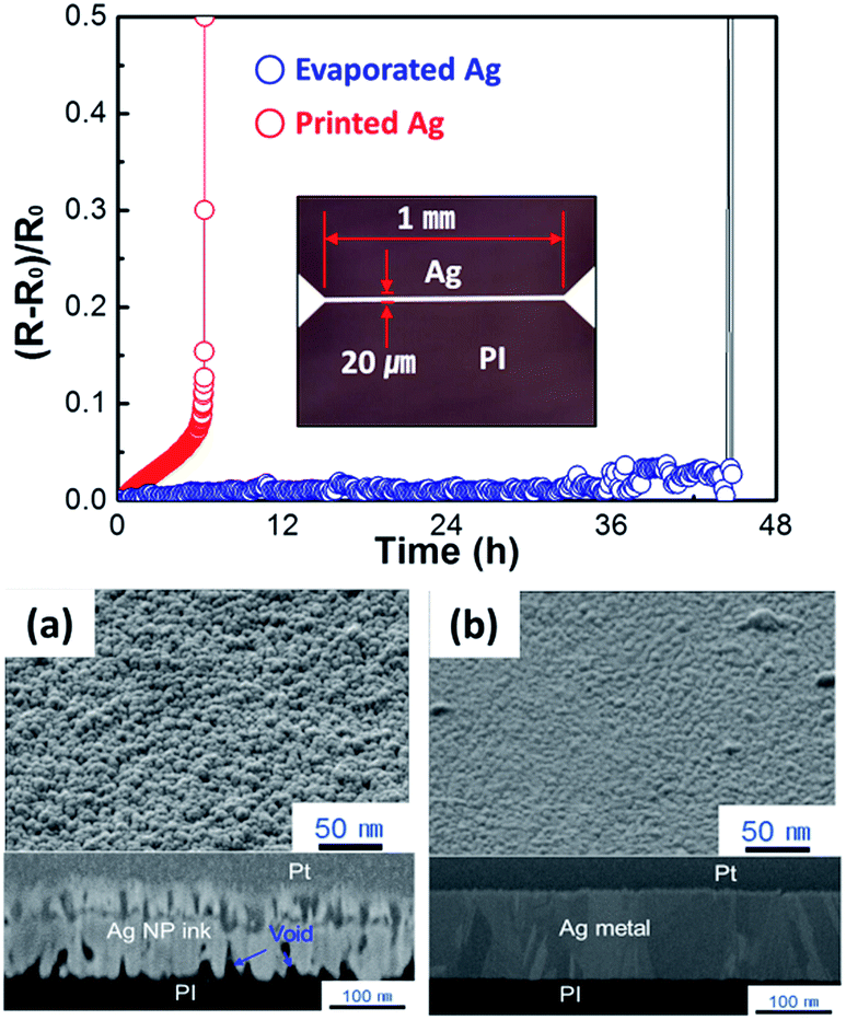 | ||
| Fig. 1 Optical pattern image of the dog-bone type sample for electromigration tests on a polyimide substrate and the percentage change in resistance under accelerated conditions for printed and evaporated Ag interconnects. SEM tilted and cross-sectional images of Ag interconnects on polyimide substrate processed by the (a) reverse offset printing method and by (b) evaporated deposition method. | ||
These pores are considered to accelerate the EM phenomenon that degrades reliability. EM phenomenon has been reported as the electron wind force drives migration of thermally active metal atoms in the direction of electron flow.22 During EM, thermally activated metal atoms migrate due to the electron wind force. Voids or hillocks are generated at the flux of the divergence sites, and metal interconnect eventually undergoes failure due to the discontinuity produced at those sites. Under elevated temperature and current stressing conditions, the pores in the Ag film function as flux divergence sites, which result in the pores growing even larger due to the EM mechanism and resulting in the electrical failure indicated by the abrupt increase in electrical resistivity. From our results, it is inferred that the necking formation and densification of Ag particles due to insufficient annealing produced a large number of pores and weak interfaces between particles. This result agrees well with the EM theory.
To understand the EM failure mechanism of a printed Ag interconnect and monitor the morphological evolution closely, the morphologies of an Ag interconnect, of which the failure time was 18 hours under the slightly lower current density of 105 A cm−2 and a temperature of 150 °C, were investigated by measuring the resistance step by step. Fig. 2 shows the morphological evolution of the interconnect at the points of 0%, 5%, 10% and 20% change in resistance. At the initial stage, Ag metal particles were uniformly distributed, and the particle size was relatively small, 10–30 nm. As the reliability test progressed, the Ag particles coarsened and grew to 20–40 nm at the point of a 5% change in resistance. This morphological change required 7 hours, at a resistance change rate of 0.7 percent per h. After the electrical resistance increased 10%, the particles had uniformly grown to 30–60 nm, and the resistance change rate remained at 0.7 percent per h. The resistance increased linearly with the elapsed time, and the particles grew uniformly. However, the electrical resistance increased rapidly once the resistance had increased by 18%, which is attributed to the abnormal particle growth throughout the Ag metal film, as seen in the sample with a 20% change in resistance.
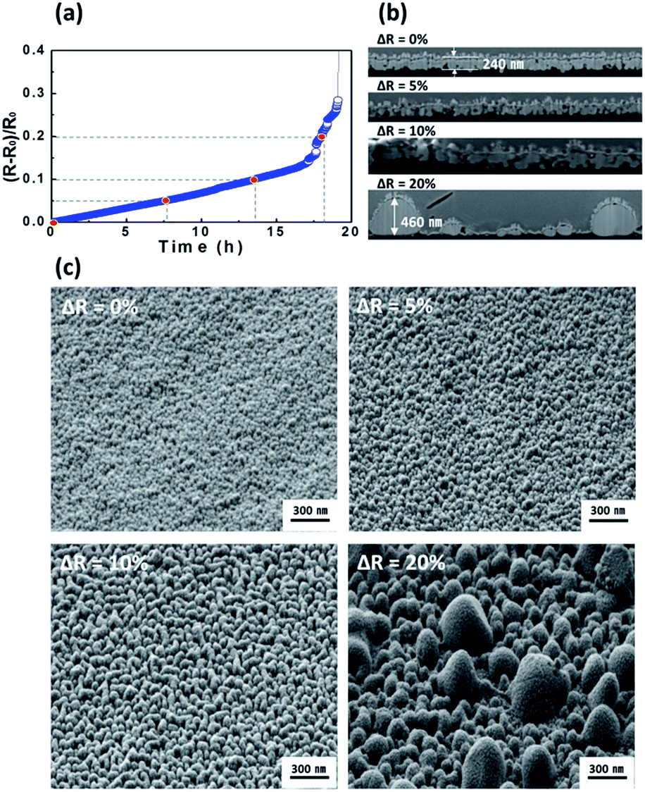 | ||
| Fig. 2 Microstructural evolution of Ag interconnects fabricated by a printing method with respect to the resistance change of 0%, 5%, 10% and 20% under the current density of 105 A cm−2: (a) resistance change of Ag interconnect. (b) Cross-section view according to the resistance change. (c) Tilt view image according to the resistance change. | ||
Even though the abnormal particle growth is the result of particle agglomeration and densification, it is harmful to the reliability since this morphological evolution generates narrower necks between particles that result in more current crowding. The Joule heat, developed around the necks due to EM, accelerates the thermal activation even more, which further increases the rate of atomic migration. The Ag atoms of the neck are consumed by the migration. Therefore, the necks become narrower and eventually break down. These disconnections result in an abrupt resistance increase at a certain point.
At the point of the 20% increase in resistance, abnormal particle growth was observed, and small-sized particles had disappeared. It is inferred that Oswald ripening of the Ag nanoparticles occurred, for which the difference in surface potential energy worked as a driving force.23 According to the Oswald ripening, atoms in small particles diffuse to large particles which eventually break the necking of the Ag particles. It is a highly noteworthy result that accelerated conditions at the relatively lower temperature (range 150–250 °C) with current stressing can produce abnormal particle growth by Oswald ripening compared to the abnormal grain growth at high temperature seen during a sintering process.
The SEM image in Fig. 3(a) after electrical failure proves that Oswald ripening occurred, as no small particles are found next to large particles, which indicates that the small particles have dissolved and the large particles have grown until failure occurred. To further investigate this phenomenon in particular, the microstructural changes of Ag interconnects were observed according to the elapsed time under accelerated current stressing. The results explained particle growth mechanism clearly. The microstructural evolution at 6, 12, 24 and 48 hours was recorded under current stressing conditions of 106 A cm−2 at 100 °C as shown in Fig. 3(b). The test was conducted at the even lower temperature than the previous cases because the resistance increase was more sensitive to increases in the temperature than it was to increases in the current density. Therefore, it was easier to observe the evolution of morphologies at the lower temperature of 100 °C. The cross-sectional image of the interconnect after 6 hours showed that there was no change in the morphology of the film. After 12 hours, a few particles had started to grow at the densely connected top region. After 24 hours, the growth of the abnormally large particles had consumed the nearby small particles due to the combined effects of minimizing surface areas and migration of thermally activated atoms to the large particles. Finally, the film consists of primarily large particles, and the small particles have almost disappeared in the Ag film after 24 hours. These results coincided with Oswald ripening phenomenon.
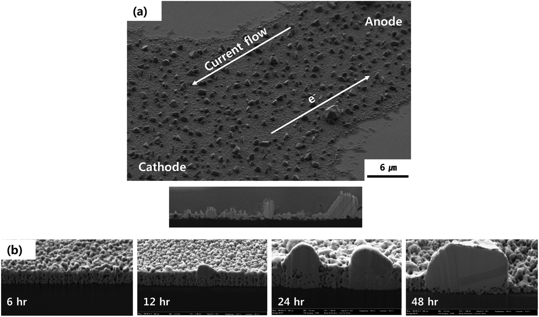 | ||
| Fig. 3 Images of the grain growth of Ag interconnects under current stressing: (a) tilt and vertical view images of current-induced facet grain growth after electrical failure. (b) Cross-section view of Ag grain evolution as a function of elapsed time at 100 °C. | ||
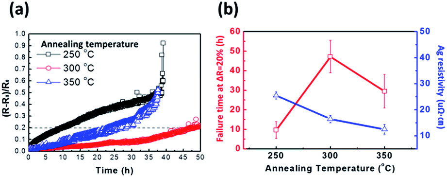
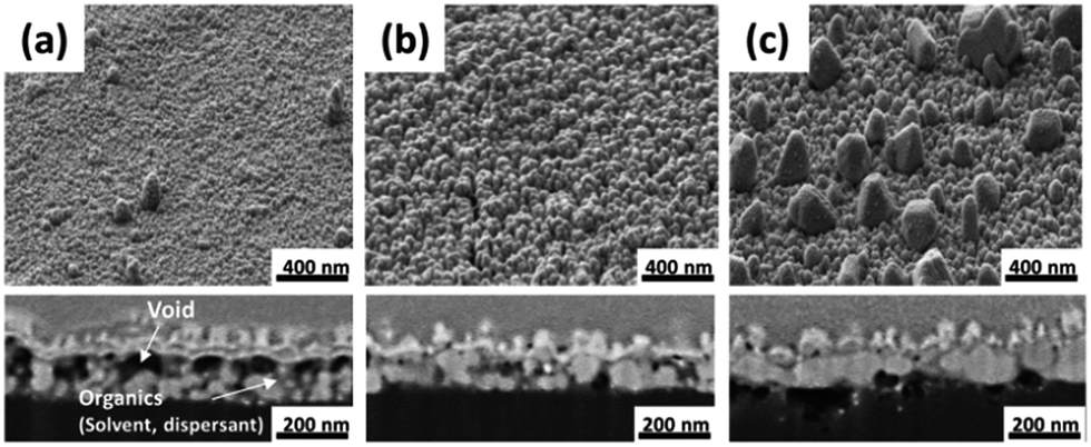
As mentioned previously, the combination of temperature and current stressing conditions was observed to affect the morphology and associated electrical reliability of the printed Ag interconnects. To determine the morphological effects on electrical reliability, the morphology and the electrical reliability of films annealed at 250, 300 and 350 °C for 30 minutes were investigated. In Fig. 4, the morphologies of Ag interconnects annealed at different temperatures are presented. To increase the density of nanoparticle films in the printed Ag interconnect, an annealing process to sinter the particles was used. The sintering mechanism proceeded through these sequential processes: first, necks formed between the Ag nanoparticles through the elimination of the organic materials. Next, densification of the film and coarsening of the particles occurred to minimize the surface energy under the applied thermal energy. Higher annealing temperatures result in denser structures. For the sample annealed at 250 °C, the average particle size was 24.3 nm with a uniform size distribution and a resistivity of 25 μΩ cm. A number of pores were found due to insufficient densification of the Ag particles. For the sample annealed at 300 °C, coarsening of the Ag particles and densification of the film were observed. Ag particles grew to an average particle size of 43.7 nm with a relatively uniform size distribution driven by the minimization of surface area. It was also confirmed that the number and size of pores were reduced, which correlates with the reduced resistivity of the interconnect of 15 μΩ cm. For the sample annealed at 350 °C, abnormal particles are observed. A few particles grew to abnormally large sizes, up to 150 nm, although small 30 nm particles were also found. This is a typical abnormal grain growth behaviour, where specific grains coarsen abruptly through secondary recrystallization due to the high thermal energy. Pores are still observed but the resistivity of the Ag drops to 12 μΩ cm due to strong neck formation and large particles. Ag interconnects annealed at the different temperatures were subjected to an accelerated stressing condition with a current density of 105 A cm−2 at 150 °C. Reliability increased with increasing annealing temperature as the electrical failure time was 9.6 hours for the sample annealed at 250 °C but increased to 46.9 hours for the sample annealed at 300 °C. However, the failure time decreased to 29.2 hours for the sample annealed at 350 °C, as shown in Fig. 5. To determine the reason for these differences, samples annealed at each of the three temperatures and subjected to the accelerated stressing condition were analysed by SEM, as shown in Fig. 6, for the specimens with a 20% change in electrical resistance. After current stressing, the 250 °C annealed sample exhibited narrow necks between the particles due to the small size of particles, leading to a large number of voids. The observed morphology shows that insufficient thermal energy was supplied to the sample during annealing to completely decompose the organic impurities and that the necks would be prone to the current crowding effect. For the sample annealed at 300 °C, the Ag film was sufficiently densified and had strong neck formation between the Ag particles, as shown in Fig. 5(b). Strong necks do not block the electrical path and better resist electrical failure under the combination of temperature and current stressing condition. However, the sample annealed at 350 °C exhibited a shorter failure time compared to the sample annealed at 300 °C due to abnormal particle growth observed in the former sample. The combination of heat and current-induced atomic migration, especially around the neck area between large and small particles, led to the failure due to size differences of Ag particles. These results mean that morphological control can affect the electrical reliability of metal interconnects. Therefore, it is important to adopt an optimized annealing condition to eliminate organic materials while maintaining a uniform particle morphology.
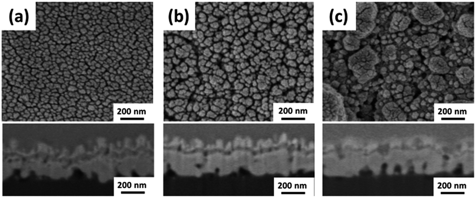 | ||
| Fig. 4 Microstructures of Ag interconnects fabricated by a printing method followed by annealing at temperature of (a) 250 °C. (b) 300 °C. (c) 350 °C. | ||
 | ||
| Fig. 5 (a) Percentage change in resistance under a current density of 105 A cm−2 for Ag interconnects annealed in different temperatures. (b) Failure time and initial resistivity of the Ag interconnects as a function of annealing temperature. | ||
 | ||
| Fig. 6 Microstructures of Ag interconnects at the 20% of resistance change under current density of 105 A cm−2. Tested samples have been annealed before testing at (a) 250 °C. (b) 300 °C. (c) 350 °C. | ||
In this work, the electrical reliability of printed Ag interconnects was investigated. Ag interconnects fabricated by the reverse offset printing method exhibited shorter electrical failure time compared to interconnects with an evaporation-deposited Ag film, showing a gradual resistance increase under elevated temperature and current stressing conditions. This phenomenon was explained with EM, which is caused by atomic displacement due to electron wind force at the flux divergence site. The combination of temperature and current stress-induced particle growth, which is attributed to atomic migration of Ag through the necks between Ag particles, leads to the current crowding effect that weakens the necks and causes abnormal particle growth. We suggest that understanding the failure mechanisms of printed interconnects can be used to develop guidelines for the production of reliable components for the next generation of electronics.
Acknowledgements
This research was supported by “Development of Interconnection System and Process for Flexible Three Dimensional Heterogeneous Devices” funded by MOTIE (Ministry of Trade, Industry and Energy) in Korea. This research was supported by the BK21PLUS SNU Materials Division for Educating Creative Global Leaders (21A20131912052).Notes and references
- F. Axisa, P. M. Schmitt, C. Gehin, G. Delhomme, E. McAdams and A. Dittmar, IEEE Trans. Inform. Tech. Biomed., 2005, 9, 325–336 CrossRef.
- H. W. Choi, T. Zhou, M. Singh and G. E. Jabbour, Nanoscale, 2015, 7, 3338–3355 RSC.
- A. C. Ferrari, F. Bonaccorso, V. Fal'ko, K. S. Novoselov, S. Roche, P. Boggild, S. Borini, F. H. L. Koppens, V. Palermo, N. Pugno, J. A. Garrido, R. Sordan, A. Bianco, L. Ballerini, M. Prato, E. Lidorikis, J. Kivioja, C. Marinelli, T. Ryhanen, A. Morpurgo, J. N. Coleman, V. Nicolosi, L. Colombo, A. Fert, M. Garcia-Hernandez, A. Bachtold, G. F. Schneider, F. Guinea, C. Dekker, M. Barbone, Z. Sun, C. Galiotis, A. N. Grigorenko, G. Konstantatos, A. Kis, M. Katsnelson, L. Vandersypen, A. Loiseau, V. Morandi, D. Neumaier, E. Treossi, V. Pellegrini, M. Polini, A. Tredicucci, G. M. Williams, B. Hee Hong, J.-H. Ahn, J. Min Kim, H. Zirath, B. J. van Wees, H. van der Zant, L. Occhipinti, A. Di Matteo, I. A. Kinloch, T. Seyller, E. Quesnel, X. Feng, K. Teo, N. Rupesinghe, P. Hakonen, S. R. T. Neil, Q. Tannock, T. Lofwander and J. Kinaret, Nanoscale, 2015, 7, 4598–4810 RSC.
- J. Perelaer, P. J. Smith, D. Mager, D. Soltman, S. K. Volkman, V. Subramanian, J. G. Korvink and U. S. Schubert, J. Mater. Chem., 2010, 20, 8446–8453 RSC.
- S. Wagner, S. P. Lacour, J. Jones, P.-h. I. Hsu, J. C. Sturm, T. Li and Z. Suo, Phys. E, 2004, 25, 326–334 CrossRef.
- M. A. Yokus, R. Foote and J. S. Jur, IEEE Sens. J., 2016, 16, 7967–7976 CrossRef.
- R. Faddoul, N. Reverdy-Bruas, A. Blayo, T. Haas and C. Zeilmann, Microelectron. Reliab., 2012, 52, 1483–1491 CrossRef CAS.
- T. T. Nge, M. Nogi and K. Suganuma, J. Mater. Chem. C, 2013, 1, 5235–5243 RSC.
- B. K. Park, D. Kim, S. Jeong, J. Moon and J. S. Kim, Thin Solid Films, 2007, 515, 7706–7711 CrossRef CAS.
- J. Suikkola, T. Björninen, M. Mosallaei, T. Kankkunen, P. Iso-Ketola, L. Ukkonen, J. Vanhala and M. Mäntysalo, Sci. Rep., 2016, 6, 25784 CrossRef CAS PubMed.
- J. Wang, R. C. Y. Auyeung, H. Kim, N. A. Charipar and A. Piqué, Adv. Mater., 2010, 22, 4462–4466 CrossRef CAS PubMed.
- K. Yasuyuki, K. Masayoshi and U. Hirobumi, J. Micromech. Microeng., 2015, 25, 045017 CrossRef.
- W. Yin, D.-H. Lee, J. Choi, C. Park and S. M. Cho, Korean J. Chem. Eng., 2008, 25, 1358–1361 CrossRef CAS.
- C. Young-Man, L. Eonseok and L. Taik-Min, J. Micromech. Microeng., 2015, 25, 075019 CrossRef.
- J. Perelaer, R. Abbel, S. Wünscher, R. Jani, T. van Lammeren and U. S. Schubert, Adv. Mater., 2012, 24, 2620–2625 CrossRef CAS PubMed.
- J.-H. Lee, N.-R. Kim, B.-J. Kim and Y.-C. Joo, Carbon, 2012, 50, 98–106 CrossRef CAS.
- J. G. Bai, Z. Z. Zhang, J. N. Calata and G. Q. Lu, IEEE Trans. Compon. Packag. Technol., 2006, 29, 589–593 CrossRef CAS.
- J. R. Greer and R. A. Street, Acta Mater., 2007, 55, 6345–6349 CrossRef CAS.
- J. Kim, B. Lee, J. Y. Lek, R. I. Made, B. Salam and C. L. Gan, Electronics Packaging Technology Conference (EPTC), IEEE 16th, 2014, pp. 27–30 Search PubMed.
- Y. J. Moon, H. Kang, K. Kang, S.-J. Moon and J. Young hwang, J. Electron. Mater., 2015, 44, 1192–1199 CrossRef CAS.
- S. Wunscher, R. Abbel, J. Perelaer and U. S. Schubert, J. Mater. Chem. C, 2014, 2, 10232–10261 RSC.
- I. A. Blech, J. Appl. Phys., 1976, 47, 1203–1208 CrossRef CAS.
- P. L. Redmond, A. J. Hallock and L. E. Brus, Nano Lett., 2005, 5, 131–135 CrossRef CAS PubMed.
Footnotes |
| † Electronic supplementary information (ESI) available: Experimental details and additional figures; current and temperature effect on electrical reliability. See DOI: 10.1039/c6ra27259b |
| ‡ These authors contributed equally to this work. |
| This journal is © The Royal Society of Chemistry 2017 |