
 Open Access Article
 This Open Access Article is licensed under a Creative Commons Attribution-Non Commercial 3.0 Unported Licence
Rapidly fabricating large-scale plasmonic silver nanosphere arrays with sub-20 nm gap on Si-pyramids by inverted annealing for highly sensitive SERS detection
Yujin Wang†
,
Yang Yang†,
Yu Sun,
Baogang Quan,
Yunlong Li,
Changzhi Gu* and
Junjie Li *
*
Beijing National Laboratory for Condensed Matter Physics, Institute of Physics, Chinese Academy of Sciences, Beijing 100190, China. E-mail: jjli@iphy.ac.cn; czgu@iphy.ac.cn; Tel: +86 10 8264 9097
First published on 16th February 2017
Abstract
A simple physical method was developed to reproducibly fabricate large-scale noble metal nanosphere arrays with controllable distribution. Different from the traditional upwards annealing process, an inverted annealing method (annealing upside down samples) is introduced to treat Ag film deposited on micro-sized Si pyramid arrays. Strikingly, high density Ag nanosphere arrays can be obtained, with the gap between the nanospheres less than 20 nm under optimized conditions, which is far superior to those made by upwards annealing. The as-formed Ag-nanospheres/Si-pyramid hybrid structure exhibited a significant high enhancement factor and highly sensitive surface enhanced Raman scattering (SERS) for Rhodamine 6G molecules. Raman mapping image of this plasmonic hybrid verified a very prominent “hot spots” effect that exists around the pyramid, which contributed mainly to an enhanced SERS signal. Our work demonstrated a feasible way to prepare high-efficiency dense plasmonic nanospheres with highly localized surface plasmon resonance response, which could be feasibly applied for other bio-sensors, and also open a potential route to fabricate a metal-coated probe for tip-enhanced Raman Spectroscopy.
Introduction
Noble metal nanostructures and their plasmonic properties have been widely utilized to modulate distribution of the incident electromagnetic field, and further achieve their widespread application in optical,1–3 chemical4,5 and biological fields.6,7 Noble metal nanoparticles (NPs), as one of the simplest nanostructures, have been extensively used to create localized surface plasmon resonance (LSPR), plus couple and form a greatly enhanced optical response by tuning the geometry and optical properties of NPs.8–11 Controllable fabrication of metal NPs is helpful for studying plasmonic properties of other complex nanostructures and for understanding the modulation mechanism and further establishing a base for their applications.Because of limited geometry sizes of the NPs, LSPR arise from the excited surface plasmon that is confined on the surface of illuminated metal NPs, which provides an enhanced electromagnetic field on the surface and in the surrounding region.12 Excitation and modulation of LSPR are influenced by many factors such as morphology, surface charge, adsorbate, and so on. When the distance between the adjacent NPs is smaller than a certain value (usually sub 10 nm), then the LSPR from adjacent NPs can couple, and the electromagnetic field is greatly localized and enhanced in the gap between the NPs, which is the so-called “hot spot” effect.13–15 These hot-spot nanostructures are widely applied in the research fields of plasmonic detection, chemical catalysis, and photovoltaic devices, especially surface enhanced Raman spectroscopy (SERS).
To enhance the LSPR effect, researchers have employed various methods to fabricate hot-spots. Although NPs were easy to acquire using sol–gel processing, and they noticeably achieved single molecule detection,16,17 metal NPs usually suffered contamination during a synthesis process, which is unfavorable for subsequent applications. It is especially hard to compress the gap between adjacent NPs into a sufficiently small value. Accurate control of physical deposition parameters allows reproducible production of metal NPs, but it is still difficult to create NPs with uniform sub 10 nm gaps, especially three-dimensional ones which are used to combine the deposition process to accommodate more NPs.18,19 In addition, thermal annealing was introduced following metal deposition in order to modify the shape, size, and distribution of the NPs.20,21 At the same time however, the gap between the NPs was enlarged and this became worse for LSPR interactions. Last but not least, modern nanofabrication techniques, such as focused ion beam (FIB) and electron beam lithography (EBL), could reproducibly and with tuning, fabricate diverse nanostructure pair arrays with sub 20 nm gaps.22,23 However, reducing the gap size is extremely difficult due to proximity effects in the EBL process and hence deteriorates field enhancement due to nonlocal effects.24,25 Fortunately, researchers observed a strong “hot spot” effect in nanodimers with sub-20 nm gaps, like the bowtie (two triangles facing each other) and disc dimers, of which the fabrication process is much easier.26,27 However, an obvious drawback to nanofabrication methods still exists; that is the difficulty of fabricating patterns over a large area, thus hindering its further practical applications for LSPR sensors. Therefore, it is crucial to find a feasible way to prepare uniform NPs with sub 20 nm gaps over a large area.
In this work, we propose a physical method to fabricate high density uniform noble metal nanospheres (NSs) by inverted annealing (annealing upside down samples) a noble metal film on a Si-pyramids substrate. This method was based on a micro-sized Si pyramid arrays substrate obtained with a chemical etching process. Distinctively, the Ag film was deposited on Si pyramid arrays, and then was annealed up-side down. It is noteworthy that uniform Ag-NSs, with ∼15 nm gaps appeared, moved towards, and gathered at the tips of pyramids after inverted annealing at 300 °C for 3 minutes. However, this high-density distribution of Ag-NSs is hard to obtain by a traditional upwards annealing process. Strong SERS spectra of Rhodamine 6G (R6G) molecules were observed on Ag-NSs/Si-pyramid nanostructures, indicating an enhanced LSPR response on this kind of substrate. Our results demonstrate a feasible way to fabricate dense plasmonic Ag-NSs with a sub-20 nm gap by inverted annealing a noble metal film on a Si-pyramids substrate; the resulting material exhibited high intensity “hot-spots” effects, thus promising future applications for biochemical and biomedical sensors. Moreover, the Ag-NSs/Si-pyramid hybrid nanostructures are good candidates for tip-enhanced Raman spectroscopy applications.
Experimental
Si-pyramids fabrication and metal nanofilms deposition
The micrometer-sized Si pyramid array substrates were fabricated by wet etching. A 60 nm thick SiNx film was pre-deposited on Si (100) substrate, and then a S1813 resist was spin-coated on the SiNx layer. The initial square resist arrays with a period of 11 μm and side length of 9 μm were obtained on the SiNx layer after UV lithography and the subsequent developing process. After that, the square patterns were transferred to the SiNx layer with reactive ion etching. Finally, a KOH solution of 20% by weight and a tetramethylammonium hydroxide (TMAH) solution (25% by weight) were successively used to etch Si at a temperature of 90 °C to obtain the double layer Si pyramid array. In addition, a step of cleaning with diluted HF solution was added to remove a possible impurity from the etching solution. Details of the fabrication process of Si pyramid arrays have been described in previous reports.28–30 Ag film was deposited on the Si pyramid with an electron beam evaporation rate of 0.2 Å s−1. By choosing a suitable thickness of Ag thin film, the deposited film was in the shape of a discontinuous nanoisland.Inverted annealing process
The metal film/Si pyramid substrates were annealed in a rapid thermal annealing oven, in which the samples were heated by lamps above and below the sample holder, sustained at a certain temperature for several minutes and then cooled down. The heating rate for the annealing process was 30 °C s−1. During the total annealing process, a thermometer (thermocouple or the infrared pyrometer) was used to monitor the temperature of the sample surface, and nitrogen was pumped into the annealing chamber as the atmosphere. In the traditionally normal annealing process, samples are placed with the structured-side up. In contrast, our samples are mounted upside down during the inverted annealing process. For simplicity, the way of annealing upside down samples is defined as inverted annealing in the following sections. In this case, the annealing temperature, duration time, and the way to mount samples are three important factors that affect the morphological change from metal nanofilms to NSs. This inverted annealing process produces metal-NSs/Si-pyramid hybrid arrays.Surface enhanced Raman scattering measurement
The noble metal-NSs/Si-pyramid hybrid nanostructures were immersed in a R6G aqueous solution with a concentration of 10−5 M for 4 h, then repeatedly washed with DI water and dried with nitrogen. For sensitivity measurements the solution's concentration was diluted to 10−9 M. SERS spectra measurements were carried out using a confocal micro-Raman spectrometer (LabRAM HR800). A 532 nm laser with a power of 0.65 mW was used as the excitation source. The laser was focused using a ×100 objective lens with the sample surface, and the scattered signals were collected with the same lens. All the samples were measured under the same conditions, and spectra were collected from several randomly selected pyramids on the substrates.Result and discussion
Characterisation and optimization of Ag-NSs/Si-pyramid hybrid nanostructure
A schematic of the fabrication process of a metal-NSs/Si-pyramid hybrid nanostructure is displayed in Fig. 1. The basic pyramid arrays were obtained on the Si substrate using UV lithography and chemical etching technology to obtain high output and low cost. One can see in the scanning electron microscope (SEM) image in Fig. 2(a), the Si pyramid arrays have a uniform size and clean surface, and are ready for subsequent metal deposition. A typical Si pyramid is exhibited in Fig. 2(b), which has the shape of a double-layer pyramid. Based on our experience that the Ag film with a thickness less than 10 nm was discontinuous on flat Si substrates, the thickness of Ag film deposited on the Si pyramid was set at less than 40 nm. As presented in Fig. 2(c), the discontinuous thin Ag film layer composed with irregular nanoislands was naturally formed on the surface of Si-pyramids after deposition.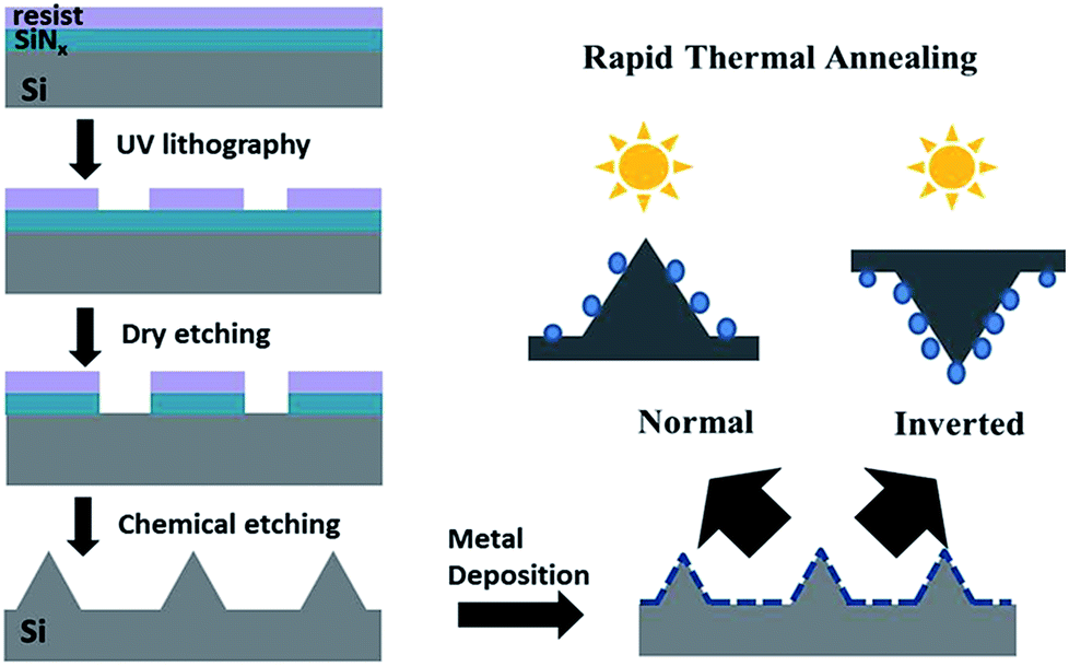 | ||
| Fig. 1 Schematic of fabrication process of metal-NSs/Si-pyramid hybrid nanostructure. | ||
 | ||
| Fig. 2 SEM images of (a) Si pyramid arrays, (b) a typical double-layer pyramid, (c) discontinuous 20 nm thick Ag thin film on a Si pyramid, (d) Ag-NSs on Si-pyramid after the normally erect annealing at 300 °C and (e) at 900 °C for 3 minutes, (f) Ag-NSs on Si-pyramid after the inverted annealing at 300 °C for 3 minutes. | ||
It is well known that the morphology of metal-NSs, including shape, sizes, and density, closely depends on annealing parameters, such as annealing temperature, duration time, and the way samples are mounted. Therefore, in our work, different annealing parameters were employed to optimize fabrication conditions of the Ag-NSs on Si-pyramids. Taking the 20 nm thick Ag film/Si-pyramid hybrid nanostructures as an example, the results were analyzed and compared after different annealing processes. When the annealing time was set constantly as 3 minutes, the Ag films were annealed at 300–500 °C and the morphology changed from irregular nanoislands into uniform NSs, while the gap between the NSs were larger than 30 nm, as shown in Fig. 2(d). The situation became worse when the temperature increased (800–900 °C). As illustrated in Fig. 2(e), the dispersed small NSs gathered into a large continuous porous film, which is similar to those observed in previous work.31 So, a moderately-high temperature (300–500 °C) was the suitable annealing temperature for the surface of nanoparticles melting and changing into a spherical shape from the irregular island shape under the surface energy. When the temperature increased, however, then large particles would absorb the smaller ones and caused a negative influence on the morphology of NSs. What was worse, the NSs would totally melt at a higher temperature (900 °C), flow on the Si pyramid and form a porous film [see Fig. 2(e)]. Additionally, annealing time is also an important factor with the morphology of NSs. If the annealing time was too short, the irregular islands would not have enough time to change into spheres. On the other hand, if the annealing time was too long, the NSs gathered together into a flat shape again. As a result, the optimized condition is annealing at 300 °C for 3 minutes.
As exhibited in Fig. 2(d), although the Ag nanoislands have changed into the more uniform Ag-NSs after rapid thermal annealing, the gaps between adjacent NSs were also enlarged during the annealing process. This phenomenon is similar to those reported in other research works, which was not favorable to the interactions of the LSPR.20,21 To solve this problem, an inverted annealing method was proposed in this work, in which samples were mounted upside down in a chamber during the traditional rapid thermal annealing process. In this way, the NSs were gathered onto the tip of the pyramid and had higher density, as shown in Fig. 2(f). What is more, the distance between the NSs was further decreased. Compared with the one under normal annealing (Fig. 2(d)), a sample had evenly distributed NSs with much higher density through inverted annealing. The results of inverted annealing are well-understood; based on the lowest energy principle, most Ag nanospheres move and gather towards the top of a pyramid to reach a more stable and lower surface energy state, which causes a higher Ag-NSs density with smaller gaps than normal annealing.
In order to further shrink the distance between NSs, the thickness of deposited Ag films was adjusted before inverted annealing. Ag films with different thicknesses (10 nm, 20 nm, and 30 nm) were deposited on a Si pyramid, respectively, and then the samples were annealed upside down. As displayed in Fig. 3(a)–(c), we can see that uniform Ag-NSs with different diameters were dispersed on the tops of the pyramids, and their diameters increased when the thickness of the deposited film increased. We randomly selected 10 pairs of NSs on the Si-pyramids of these three samples, respectively, and estimated the average gaps between NSs. As shown in Fig. 3(d), the average gap of a 10 nm thick sample was only around 14 nm, much smaller than the other two samples (35 nm and 43 nm). The distance between Ag-NSs on the Si pyramid deposited with 10 nm thick Ag film was smaller than 20 nm, along with rather high distributing density, which was within the critical value to achieve “hot spots”. It is worthwhile to note that a single Ag-NS can be formed and just located at the tip of the pyramid, which is advantageous in a tip-enhanced plasmonic property.
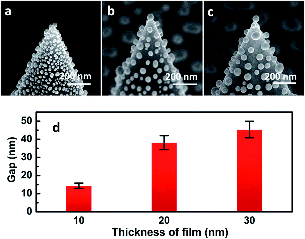 | ||
| Fig. 3 SEM images of a Ag-NSs/Si pyramid with Ag film in different thicknesses: (a) 10 nm, (b) 20 nm, (c) 30 nm after inverted annealing at 300 °C for 3 minutes. (d) Average value of the gaps between adjacent NSs on the Si pyramid as a function of the thicknesses of deposited Ag films. | ||
Herein, we can summarize that the controllable morphology of Ag-NSs is successively achieved by inverted annealing metal thin films on the top of Si-pyramids, in which 10 nm thick Ag film is the most suitable for fabricating a large-area equally-distributed sub-20 nm gap, which is very favourable to producing so-called “hot spots” with high density. With these hot spots, the Ag-NSs/Si-pyramid hybrid nanostructure is suitable for plasmonic detection, especially by SERS spectra measurements.
The LSPR properties and highly-sensitive SERS of Ag-NSs/Si-pyramid hybrid nanostructures
To investigate LSPR properties of Ag-NSs/Si-pyramid hybrid nanostructures, Raman spectra of R6G molecules were measured on samples with different treatments (pristine, normal annealing, and inverted annealing) and compared in Fig. 4(a). The inverted annealed one exhibits the strongest SERS signal, and it is much higher than two others in Raman intensity. The intensity of a Raman characteristic peak at 613 cm−1 of R6G molecules on the normal and inverted annealing samples was 16 and 28 times larger than that without annealing. Compared to previous irregular nanoislands in the sample without annealing, the size of Ag-NSs became more uniform after annealing, and thus the plasmon resonance frequency of the spherical particles was more consistent, which caused the local electric field and corresponding Raman signals of molecules absorbed nearby to be stronger. Except for the above advantage, the density of Ag-NSs on the inverted annealed sample was much higher than that on a normally annealed one, which lead to strong electromagnetic coupling between the adjacent NSs, and thus achieved the highest enhancement of Raman signals among the three kinds of samples.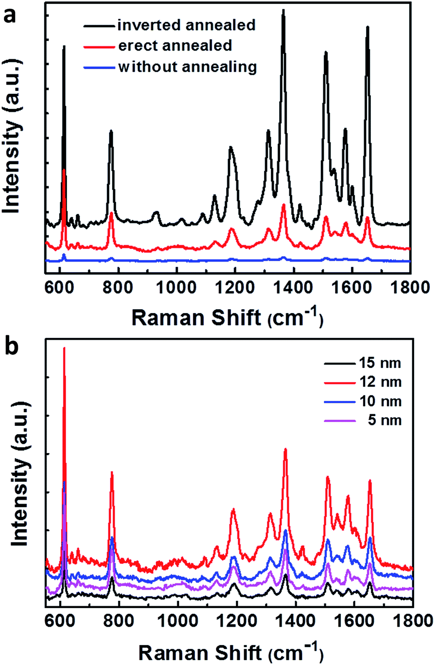 | ||
| Fig. 4 (a) SERS spectra of R6G molecules on Ag-NSs/Si pyramid hybrid samples under different treatments: without annealing, normal erect annealing, and inverted annealing. (b) SERS spectra of R6G molecule on Ag-NSs/Si-pyramid hybrid samples as a function of the thickness of deposited Ag film. | ||
Although the gap between Ag-NSs could be tuned to around 15 nm by keeping the thickness of deposited Ag film at around 10 nm, more efforts are still needed to get the highest LSPR effect. Therefore, further optimizing the thickness of Ag film was taken as an action. Ag films with thicknesses of 5 nm, 10 nm, 12 nm, and 15 nm were deposited on Si-pyramids, respectively, and were inverted and annealed at 300 °C for 3 minutes. Then, SERS measurements were made on these four samples respectively, and the results are shown in Fig. 4(b). One can see clearly that the Ag-NSs/Si-pyramid hybrid formed from 12 nm thick Ag film has the highest SERS intensity, suggesting the highest LSPR response. Remarkably, taking the peak at 613 cm−1 as a reference, the SERS intensity on the Ag-NSs/Si-pyramid from 12 nm thick Ag film is 2.32 times larger than that of the one fabricated from 10 nm thick Ag film, and is enhanced 4 times as compared with the samples under normal annealing. Moreover, as suggested in Fig. 4(b), there is an only a very narrow window for the fabrication of Ag-NSs with the highest LSPR effect.
Then, in order to see the special distribution of LSPR response on the Ag-NSs/Si-pyramid hybrid nanostructure fabricated from 12 nm thick Ag film, Raman mapping measurements with a step size of 0.5 μm were performed on a 5 × 5 μm2 area centered around a single Ag-NSs/Si-pyramid, as shown in Fig. 5(a) and (b). The Raman mapping image was created using the integral intensity of the peak at 612 cm−1, and is presented in Fig. 5(c). It is notable that the highest SERS intensity appears in the center of that image, in which a diamond-shape pattern clearly can be seen, corresponding to an intense “hot-spots” effect. Interestingly, the blue diamond pattern in the mapping image shows good agreement with the top view of the zone at the tip of the pyramid. Moreover, a dark blue cross can be seen along the diagonal lines of the dashed diamond, which overlapped with the four ridges of the pyramid, indicating the highest LSPR effect arises at the ridges of the pyramid. As we know, the LSPR would be enhanced on the tip and edges of nanostructures.32,33 In our work, the ridges of a pyramid would be a kind of edges where LSPR would become stronger due to the enhanced locality of surface plasmon. The mapping result indicates the homogeneous distribution of the LSPR effect on the Ag-NSs/Si-pyramid hybrid nanostructures, and also testifies to our previous results that the area located by an Ag-NSs/Si-pyramid hybrid holds the highest LSPR on the whole substrate.
 | ||
| Fig. 5 (a) SEM image, (b) optical image and (c) Raman mapping image of a single Ag-NSs/Si pyramid obtained by inverted annealing the substrate deposited with 12 nm thick Ag film. The square in (b) shows the area selected for mapping measurements. The dashed line in (c) indicates the zone of the tip. The scale bar inset is 1 μm. | ||
To further investigate the SERS properties of the Ag-NSs/Si-pyramid hybrid nanostructures, measurements for sensitivity and repeatability were carried out. As is shown in Fig. 6(a), when the R6G solution was diluted, the intensity of the characteristic Raman peak decreased. However, the peaks from R6G were still clearly distinguishable even when the concentration was as low as 10−9 M. From an enlarged SERS signal inserted in Fig. 6(a), all the featured Raman peaks of R6G can be seen clearly, indicating that this substrate has the potential for highly-sensitive molecule detection. To evaluate the repeatability and uniformity of the SERS signals, one of the pyramids was randomly chosen on the substrate for measurement, and the Raman spectra of R6G molecules on each as-chosen pyramid were measured every two hours. As shown in Fig. 6(b), the consistent SERS spectra demonstrated the signal on the hybrid NSs has good homogeneity over the whole substrate, indicating the possibility of further practical applications as a plasmonic detection device.
 | ||
| Fig. 6 (a) SERS signals of R6G with different concentrations on the Ag-NSs/Si-pyramid hybrid nanostructures fabricated by inverted annealing the substrate coated with 12 nm thick Ag film, and the inset is an enlarged SERS signal at 10−7 and 10−9 M. (b) Homogeneity measurement of SRES signals on five randomly selected Ag-NSs/Si-pyramids. | ||
The SERS results in our work demonstrate that Ag-NSs/Si-pyramid hybrid nanostructures could produce a highly intense “hot-spot” effect, also suggesting its potential applications for tip-enhanced Raman spectroscopy (TERS). So far, fabricating reliable and high-efficiency TERS tips is still a challenge with development of the TERS technique. Although various fabricating methods have been employed in past years, coating a noble metal film on atomic force microscope (AFM) tips is the most commonly used method to fabricate TERS tips.34,35 This simple and reproducible method developed in our work puts forward a new route for fabricating probes for tip-enhanced Raman spectroscopy.
Conclusions
A new method was demonstrated to fabricate Ag-NSs with uniform size and high density on the Si pyramid by inversely upside down annealing, which improves significantly the undesirable distribution of Ag-NSs annealed by the traditional upwards mode. Noteworthy, the gap between adjacent NSs on the Si pyramid can be kept smaller than 20 nm, leading to a high density and intense “hot spot” effect. The Ag-NSs/Si-pyramid plasmonic hybrid nanostructure was used as SERS substrates, and showed a highly intense SERS signal of R6G molecules, together with high sensitivity and homogeneity of the SERS signal, indicating an ideal candidate for SERS detecting applications. This simple and reproducible method also puts forward a new route for fabricating probes for tip-enhanced Raman spectroscopy with optimized morphology at the tips that then results in higher LSPR response.Acknowledgements
The authors acknowledge the Ministry of Science and Technology of China (Grant no. 2016YFA0200803, 2016YFB0100500, 2016YFA0200402), the National Natural Science Foundation of China (Grant no. 91323304, 11674387, 61390503, 11574369), and Strategic Priority Research Program of the Chinese Academy of Sciences under Grant no. XDB07020200.Notes and references
- V. E. Ferry, L. A. Sweatlock, D. Pacifici and H. A. Atwater, Plasmonic nanostructure design for efficient light coupling into solar cells, Nano Lett., 2008, 8(12), 4391–4397 CrossRef CAS PubMed.
- M. W. Knight, Y. Wang, A. S. Urban, A. Sobhani, B. Y. Zheng, P. Nordlander and N. J. Halas, Embedding plasmonic nanostructure diodes enhances hot electron emission, Nano Lett., 2013, 13(4), 1687–1692 CrossRef CAS PubMed.
- S. Linic, P. Christopher and D. B. Ingram, Plasmonic-metal nanostructures for efficient conversion of solar to chemical energy, Nat. Mater., 2011, 10(12), 911–921 CrossRef CAS PubMed.
- J. B. Lassiter, H. Sobhani, J. A. Fan, J. Kundu, F. Capasso, P. Nordlander and N. J. Halas, Fano resonances in plasmonic nanoclusters: geometrical and chemical tunability, Nano Lett., 2010, 10(8), 3184–3189 CrossRef CAS PubMed.
- P. Christopher, H. Xin and S. Linic, Visible-light-enhanced catalytic oxidation reactions on plasmonic silver nanostructures, Nat. Chem., 2011, 3(6), 467–472 CAS.
- A. Kuzyk, R. Schreiber, Z. Fan, G. Pardatscher, E.-M. Roller and A. Högele, et al., DNA-based self-assembly of chiral plasmonic nanostructures with tailored optical response, Nature, 2012, 483(7389), 311–314 CrossRef CAS PubMed.
- Y. B. Zheng, B. Kiraly, P. S. Weiss and T. J. Huang, Molecular plasmonics for biology and nanomedicine, Nanomedicine, 2012, 7(5), 751–770 CrossRef CAS PubMed.
- J. F. Li, Y. F. Huang, Y. Ding, Z. L. Yang, S. B. Li and X. S. Zhou, et al., Ecologically distinct dinosaurian sister group shows early diversification of Ornithodira, Nature, 2010, 464(7285), 392–395 CrossRef CAS PubMed.
- J. Y. Lu, G. L. Liu and L. P. Lee, High-density silver nanoparticle film with temperature-controllable interparticle spacing for a tunable surface enhanced Raman scattering substrate, Nano Lett., 2005, 5(1), 5–9 CrossRef PubMed.
- C. E. Talley, J. B. Jackson, C. Oubre, N. K. Grady, C. W. Hollars and S. M. Lane, et al., Surface-enhanced Raman scattering from individual Au nanoparticles and nanoparticle dimer substrates, Nano Lett., 2005, 5(8), 1569–1574 CrossRef CAS PubMed.
- G. Chen, Y. Wang, M. Yang, J. Xu, S. J. Goh and P. Ma, et al., Measuring ensemble-averaged surface-enhanced Raman scattering in the hotspots of colloidal nanoparticle dimers and trimers, J. Am. Chem. Soc., 2010, 132(11), 3644–3645 CrossRef CAS PubMed.
- K. A. Willets and R. P. Van Duyne, Localized surface plasmon resonance spectroscopy and sensing, Annu. Rev. Phys. Chem., 2007, 58(58), 267–297 CrossRef CAS PubMed.
- W. D. Li, F. Ding, J. Hu and S. Y. Chou, Three-dimensional cavity nanoantenna coupled plasmonic nanodots for ultrahigh and uniform surface-enhanced Raman scattering over large area, Opt. Express, 2011, 19(5), 3925–3936 CrossRef PubMed.
- F. S. Ou, M. Hu, I. Naumov, A. Kim, W. Wu and A. M. Bratkovsky, et al., Hot-spot engineering in polygonal nanofinger assemblies for surface enhanced Raman spectroscopy, Nano Lett., 2011, 11(6), 2538–2542 CrossRef CAS PubMed.
- Z. Hu, Z. Liu, L. Li, B. Quan, Y. Li and J. Li, et al., Plasmonic Coupling: Wafer-Scale Double-Layer Stacked Au/Al2O3@Au Nanosphere Structure with Tunable Nanospacing for Surface-Enhanced Raman Scattering, Small, 2014, 10(19), 3933–3942 CrossRef CAS PubMed.
- K. Kneipp, Y. Wang, H. Kneipp, L. T. Perelman, I. Itzkan and R. Dasari, et al., Single Molecule Detection Using Surface-Enhanced Raman Scattering (SERS), Phys. Rev. Lett., 1997, 78(9), 1667–1670 CrossRef CAS.
- S. Nie and S. R. Emory, Probing single molecules and single nanoparticles by surface-enhanced Raman scattering, Science, 1997, 275(5303), 1102–1106 CrossRef CAS PubMed.
- Y. J. Oh and K. H. Jeong, Glass nanopillar arrays with nanogap-rich silver nanoislands for highly intense surface enhanced Raman scattering, Adv. Mater., 2012, 24(17), 2234–2237 CrossRef CAS PubMed.
- M. S. Schmidt, J. Hübner and A. Boisen, Nanopillars: Large Area Fabrication of Leaning Silicon Nanopillars for Surface Enhanced Raman Spectroscopy, Adv. Mater., 2012, 24(10), 11–18 Search PubMed.
- K. Kim, J. W. Choi, K. Ma, R. Lee, K. H. Yoo and C. O. Yun, Nanoisland-Based Random Activation of Fluorescence for Visualizing Endocytotic Internalization of Adenovirus, Small, 2010, 6(12), 1293–1299 CrossRef CAS PubMed.
- H. Liu, X. Zhang, T. Zhai, T. Sander, L. Chen and P. J. Klar, Centimeter-scale-homogeneous SERS substrates with seven-order global enhancement through thermally controlled plasmonic nanostructures, Nanoscale, 2014, 6(10), 5099–5105 RSC.
- J. Zhang, M. Irannejad and B. Cui, Bowtie Nanoantenna with Single-Digit Nanometer Gap for Surface-Enhanced Raman Scattering (SERS), Plasmonics, 2015, 10(4), 831–837 CrossRef CAS.
- N. A. Hatab, C. H. Hsueh, A. L. Gaddis, S. T. Retterer, J. Li and G. Eres, Free-Standing Optical Gold Bowtie Nanoantenna with Variable Gap Size for Enhanced Raman Spectroscopy, Nano Lett., 2010, 10(12), 4952–4955 CrossRef CAS PubMed.
- F. J. García de Abajo, Nonlocal Effects in the Plasmons of Strongly Interacting Nanoparticles, Dimers, and Waveguides, J. Phys. Chem. C, 2008, 112(46), 17983–17987 Search PubMed.
- A. I. Fernández-Domínguez, A. Wiener, F. J. García-Vidal, S. A. Maier and J. B. Pendry, Transformation-Optics Description of Nonlocal Effects in Plasmonic Nanostructures, Phys. Rev. Lett., 2012, 108(10), 106802–106805 CrossRef PubMed.
- A. Gopinath, S. V. Boriskina, B. M. Reinhard and L. D. Negro, Deterministic aperiodic arrays of metal nanoparticles for surface-enhanced Raman scattering (SERS), Opt. Express, 2009, 17(5), 3741–3753 CrossRef CAS PubMed.
- P. J. Schuck, D. P. Fromm, A. Sundaramurthy, G. S. Kino and W. E. Moerner, Improving the mismatch between light and nanoscale objects with gold bowtie nanoantennas, Phys. Rev. Lett., 2005, 94(1), 017402–017404 CrossRef CAS PubMed.
- K. Biswas and S. Kal, Etch characteristics of KOH, TMAH and dual doped TMAH for bulk micromachining of silicon, Microelectron. J., 2006, 37(6), 519–525 CrossRef CAS.
- A. Brockmeier, F. J. S. Rodriguez, M. Harrison and U. Hilleringmann, Surface tension and its role for vertical wet etching of silicon, J. Micromech. Microeng., 2012, 22(22), 1519–1529 Search PubMed.
- K. Rola and I. Zubel, Micromirrors inclined at 45o towards Si substrates fabricated by anisotropic etching, Opt. Appl., 2011, 41(2), 423–430 Search PubMed.
- L. H. Qian, X. Q. Yan, T. Fujita, A. Inoue and M. W. Chen, Surface enhanced Raman scattering of nanoporous gold: smaller pore sizes stronger enhancements, Appl. Phys. Lett., 2007, 90(15), 153120–153123 CrossRef.
- X. Chen, N. C. Lindquist, D. J. Klemme, P. Nagpal, D. J. Norris and S. H. Oh, Split-Wedge Antennas with Sub-5 nm Gaps for Plasmonic Nanofocusing, Nano Lett., 2016, 16(12), 7849–7856 CrossRef CAS PubMed.
- W. Yue, Y. Yang, Z. Wang, L. Chen and X. Wang, Surface-enhanced Raman scattering on gold nanorod pairs with interconnection bars of different widths, Sens. Actuators, B, 2012, 171–172, 734–738 CrossRef CAS.
- B. S. Yeo, W. Zhang, C. Vannier and R. Zenobi, Enhancement of Raman Signals with Silver-Coated Tips, Appl. Spectrosc., 2006, 60(10), 1142–1147 CrossRef CAS PubMed.
- L. K. Yang, T. X. Huang, Z. C. Zeng, M. H. Li, X. Wang and F. Z. Yang, et al., Rational fabrication of a gold-coated AFM TERS tip by pulsed electrodeposition, Nanoscale, 2015, 7(43), 18225–18231 RSC.
Footnote |
| † These authors contributed equally to this work. |
| This journal is © The Royal Society of Chemistry 2017 |