
 Open Access Article
 This Open Access Article is licensed under a Creative Commons Attribution-Non Commercial 3.0 Unported Licence
Flexible and low-voltage organic phototransistors
Fanfan Yua,
Shaohua Wua,
Xiaohong Wang*ab,
Guobing Zhanga,
Hongbo Luab and
Longzhen Qiu *ab
*ab
aKey Lab of Special Display Technology, Ministry of Education, National Engineering Lab of Special Display Technology, State Key Lab of Advanced Display Technology, Academy of Opto-Electronic Technology, Hefei University of Technology, Hefei, 230009, People's Republic of China. E-mail: xhwang11@hfut.edu.cn; lzhqiu@hfut.edu.cn
bKey Laboratory of Advanced Functional Materials and Devices, School of Chemistry and Chemical Engineering, Hefei University of Technology, Anhui Province, People's Republic of China
First published on 15th February 2017
Abstract
A stripping procedure was demonstrated for the preparation of an ultra-smooth aluminum electrode. After potentiostatic anodization and treatment with a self-assembled monolayer (SAM) of n-octadecyl phosphonic acid, AlOx–SAM hybrid dielectrics were grown onto flexible, stripped aluminum combining low cost manufacture under ambient conditions with excellent dielectric characteristics (negligible leakage, 114.3 nF cm−2 capacitance). Field effect transistors using dinaphtho[2,3-b:2′,3′-f]thieno[3,2-b]thiophene (DNTT) as an organic semiconductor can be operated below −5 V with a high mobility of 0.53 cm2 V−1 s−1, high on/off current ratio of 1.7 × 10⁵, low subthreshold slope of 210 mV dec−1, and good threshold of −1.51 V. Moreover, the DNTT transistor showed a good photoresponse to blue light with a wavelength of 450 nm, with photoresponsivity (R) of 50 A W−1 and a photocurrent/dark current ratio (P) of 5 at a light intensity of 5 μW cm−2.
Introduction
Organic field effect transistors (OFETs) have attracted tremendous attention due to their advantages such as low cost, light weight, and high flexibility.1 They cannot only be used to construct integrated circuits2 and backplanes,3 but also offer excellent possibilities for use as sensors.4 Phototransistors that can detect optical signals and convert optical variation into an electrical signal are one of the major applications of OFETs. The internal signal amplification function of the transistor device endows phototransistors with high photosensitivity and low noise.5 Great strides have been made over the last decades in the development of organic phototransistors (OPTs) with photoresponsivity (R) up to 104 A W−1 and photosensitivity, also called photocurrent/dark-current ratio, (P) over 105, exceeding those of Si-based phototransistors (R ≈ 300 A W−1 and P ≈ 103). However, there are still a lot of technical difficulties to be solved for commercial applications of OPTs.4a,b One of the key challenges comes from the high operating voltages of OFETs, often exceeding 20 V, which leads to excessive energy consumption and poor integration capability to the terminal product.6 Therefore, successful implementation of the phototransistor technology in future generations of optical sensors not only requires the development of high performance device architectures but also needs the demonstration of low operating voltage organic phototransistors.Generally, the operating voltage of an OFET can be decreased by increasing the capacitance density of the gated dielectric. According to the formula of capacitance, Ci = εoκ/d, a large Ci can be achieved either by increasing the dielectric constant (κ) or by decreasing the thickness (d) of dielectric films.7 Therefore, OFETs driven by a relatively low voltage can be fabricated by increasing the capacitance of the gate insulating film using self-assembled monolayers (SAMs),8 high-κ inorganic insulating films,9 cross-linked organic insulating polymers,10 or ionic liquids.11 Among them, hybrid gate dielectrics composed of self-assembled monolayers8 or multilayers12 on ultrathin inorganic oxides have proven to be excellent candidates for low-voltage OTFTs.13 The oxide–SAM hybrid gate dielectrics with thickness of a few nanometers can provide high capacitances above 500 nF cm−2 for operating voltages below 2 V, while still maintaining the leakage current as low as 1 × 10⁻⁸ A cm−2.6,14 In order to grow metal oxide films with nanometer control, electrochemical oxidation, also named as anodization, is a good, effective and solution based technique. The self-healing nature15 of the anodic oxide allows fabricating high performance devices on industrial-scale plastic substrates with considerable surface roughness. Especially, aluminum oxide (AlOx) prepared by anodization has attracted tremendous attention for its high dielectric constant, low leakage current, low cost and environmental friendly process.14
It is reported the variation in dielectric thickness and roughness surface can severely reduce the mobility of OFET device with ultrathin gate dielectrics.16 A recent study17 revealed such degradation is mainly caused by the charge scattering at the rough interface. Therefore, a properly designed smooth and continuous interface is essential in achieving optimum OFET performance. In this study, a stripping procedure was reported to prepare a smooth aluminum gate electrode with a mean roughness less than 1 nm. AlOx–SAM hybrid dielectrics were prepared using potentiostatic anodization and the following modification with n-octadecyl phosphonic acid. The field-effect characteristics as well as photoresponse of organic transistors with dinaphtho[2,3-b:2′,3′-f]thieno[3,2-b]thiophene (DNTT) as organic semiconductor18 were investigated as well.
Results and discussion
The stripping procedure for preparing aluminum electrode with ultra-smooth surface on flexible substrates was shown in Fig. 1. First, polystyrene (PS) was spin coated as a sacrificial layer on cleaned Si wafer at speed of 5000 rpm for 40 s (Fig. 1b). Then an aluminium layer was thermally evaporated onto the PS films (Fig. 1c). Flexible polyethylene terephthalate (PET) film coated with a UV-curing adhesive (UVAB) was covered on the aluminium surface. The adhesive layer was then solidified by using 365 nm UV-light for 10 min (Fig. 1d). After putting into cyclohexane for 1 h to remove the PS films, the aluminium layer buried in the UV-curing adhesive layer was separated from Si wafer (Fig. 1e). Finally, the ultra-smooth bottom surface of aluminum was fabricated and the composite films were flexible (Fig. 1f).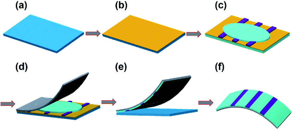 | ||
| Fig. 1 Schematic description for the tripping procedure for fabricating flexible and ultra-smooth aluminium. | ||
Atomic force microscope (AFM) and scanning electron microscopy (SEM) were applied to characterize the morphology of the aluminum surface. SEM images showed that the top surface of the as-deposited aluminum have a lot of particles (Fig. 2a), while the stripped bottom surface of the aluminum is quite smooth (Fig. 2b). AFM images revealed that the as-deposited aluminum films consist of small grains (∼100–200 nm) separated by deep grain boundaries (∼10 nm) (Fig. 2c). Apparently, the stripped bottom surface of aluminum is much smoother than the as deposited top surface (Fig. 2d). Root mean square roughness (Rq) was also calculated to characterize the smoothness of the surface. The Rq of the as-deposited top surface of the aluminum is 3.95 nm which is much higher than the Rq of 0.91 nm for the stripped bottom surface.
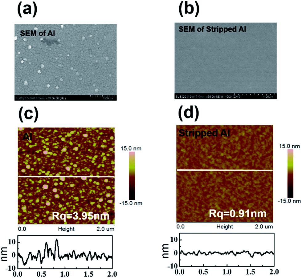 | ||
| Fig. 2 (a) SEM image of as-deposited aluminum on glass, (b) SEM image of stripped aluminum on PET, (c) AFM image of as-deposited aluminum on glass, (d) AFM image of stripped aluminum on PET. | ||
Potentiostatic anodization is adopted to achieve AlOx with controlled thickness.19 Fig. 3a showed cross-sectional FETEM image of oxide aluminum anodized at 10 V for 600 s. There is a clear boundary between aluminum layer and AlOx layer. A uniform AlOx layer with thickness about 32 nm is observed. Energy-dispersive X-ray (EDX) was used to analyze element of each layers. Fig. 3b and c demonstrated that AlOx layer was successfully prepared. Fig. 3d and e are the AFM images of the surface of the AlOx layer prepared on as-deposited surface and stripped surface. The Rq of the AlOx on the as-deposited surface is 5.20 nm and the Rq of the AlOx on the stripped surface is 1.50 nm. Compared to the surface of aluminum, the roughness, the height of the particle and the diameter of the granule on the anodized AlOx increased slightly, which is similar to the results reported in ref. 14 and 16a.
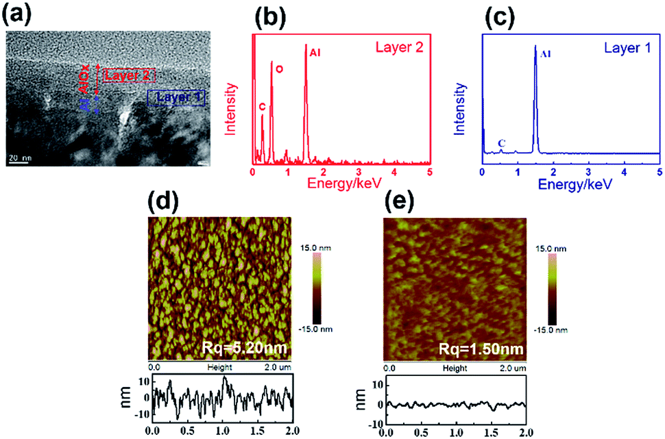 | ||
| Fig. 3 (a) High-resolution cross-sectional FETEM image of the AlOx on stripped Al prepared by potentiostatic anodization, (b and c) EDX analysis on the selective area in (a). (d) AFM image of the anodized AlOx on as-deposited Al. (e) AFM image of the anodized AlOx on stripped Al. | ||
The metal–insulator–metal (MIM) structure was used to assess the dielectric properties leakage current density (Jleak) and capacitance density (Ci) characteristics.20 For comparison, the surfaces of the as-prepared aluminum and the stripped aluminum were oxidized by O3 plasma and potentiostatic anodization, respectively, and then were modified with self-assembled monolayer of n-octadecyl phosphonic acid. The specific conditions of the four dielectrics fabricated by different ways were listed in Table 1. Current density vs. voltage and capacitance density vs. frequency were measured and showed in Fig. 4a and b. It can be seen that the current density of both dielectrics oxidized by oxygen plasma (sample 1 and 2) increased rapidly as the increase of voltage. The Jleak at 2 V was about 10−4 A cm−2. Although the Jleak of plasma grown AlOx in our work was much poorer than that reported by Klauk,21 it was comparable with the result reported by Acton8d which indicated that tremendous optimizations were required for the application of the plasma grown AlOx with thickness about 4.0 nm as a dielectric layer. Remarkably, anodized AlOx on stripped aluminum (sample 4) reduced Jleak by nearly three orders of magnitude to 10−7 A cm−2 at an applied voltage of 2 V. In contrast, anodized AlOx on as-deposited aluminum (sample 3) only reduced Jleak by about two orders of magnitude to 10−6 A cm−2. The significant small Jleak of sample 4 compared to sample 3 was likely from the combination of a more homogeneous AlOx layer with a more closely packed SAM derived from the ultra-smooth stripped aluminum. The low Jleak of AlOx–SAM hybrid dielectrics prepared on stripped aluminum via anodization make it as good gate dielectrics. The Ci characteristics between 100 Hz and 100 kHz of four AlOx–SAM hybrid dielectrics are presented in Fig. 4b. The capacitance density of AlOx–SAM hybrid dielectrics prepared on stripped aluminum via anodization is 0.114 μF cm−2. Assuming a permittivity of 2.5 and a thickness of 2.1 nm for the SAM as reported in literature6,22 and a measured thickness of 32 nm for the aluminium oxide, the permittivity of AlOx was calculated as ε = 4.6 according to the formulation: 1/Ctotal = 1/CSAM + 1/CAlOx, which agreed with the reported value of ε for thin aluminum oxide films.7
| Aluminum surface | Dielectric treatment | Surface modification | |
|---|---|---|---|
| Dielectric 1 | As-deposited | O3 plasma | n-Octadecyl phosphonic acid |
| Dielectric 2 | Stripped | O3 plasma | n-Octadecyl phosphonic acid |
| Dielectric 3 | As-deposited | Anodization | n-Octadecyl phosphonic acid |
| Dielectric 4 | Stripped | Anodization | n-Octadecyl phosphonic acid |
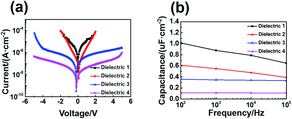 | ||
| Fig. 4 (a) Current density as a function of voltage for four samples. (b) Capacitance density as a function of frequency for four samples. | ||
The bottom-gate and top-contact configuration was used to fabricate four types of devices. Aluminum was used as gate electrode, AlOx hybrid dielectrics grown on it were used as gate insulator. After thermal deposition of DNTT semiconductor layer, Au was deposited as source and drain electrode. The stripped aluminum on PET substrate shows very good flexibility (Fig. 5a). Fig. 5b–i showed the transfer and output curve of OTFTs based on different kinds of AlOx–SAM dielectric layers listed in Table 1. Because all four AlOx–SAM dielectrics have relative high capacitance density ranging from 1.01 to 0.114 μF cm−2, their OTFTs can operate at a relative low voltage below −5 V. The AlOx–SAM prepared from anodization is much thicker than that prepared from O3 treatment; the OTFT devices based on dielectric 3 and 4 can withstand higher voltage than dielectric 1 and 2. Moreover, the gate leakage currents of anodized AlOx–SAM were one order of magnitude smaller than plasma grown AlOx–SAM from the same substrate. The mobility, threshold voltage (Vth), on/off current ratio (Ion/off), subthreshold swing (SS) were calculated and compared in Table 2. The OTFTs based on the anodized AlOx–SAM hybrid dielectrics prepared on stripped aluminum exhibited the highest mobility of 0.53 cm2 V−1 s−1 with a Vth of −1.51 V, an Ion/off of 1.7 × 10⁵ and a SS value of 210 mV dec−1.
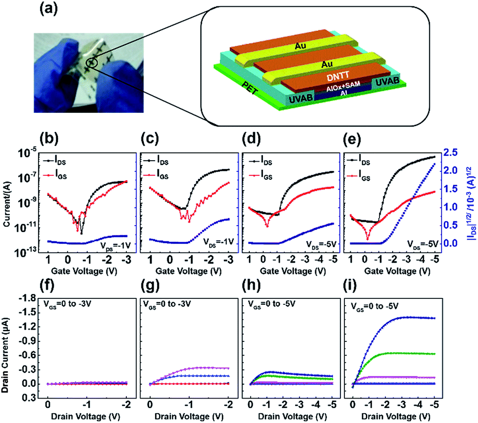 | ||
| Fig. 5 (a) Photograph of the flexible OTFTs and schematic view of a top contact device using Al as the gate electrode and n-octadecyl phosphonic acid self-assembled monolayer modified AlOx as the gate dielectric. (b–i) Typical output and transfer characteristics of OTFTs of the four types of dielectrics. | ||
| Dielectric | Average mobility (cm2 V−1 s−1) | Max mobility (cm2 V−1 s−1) | Vth (V) | Ion/off | SS (V dec−1) |
|---|---|---|---|---|---|
| Dielectric 1 | 5.3 × 10⁻³ | 7.4 × 10⁻³ | −0.85 | 1.2 × 10⁴ | −0.13 |
| Dielectric 2 | 3.9 × 10⁻² | 5.0 × 10⁻² | −0.95 | 1.1 × 10³ | −0.22 |
| Dielectric 3 | 1.1 × 10⁻² | 2.3 × 10⁻² | −1.00 | 1.2 × 10⁴ | −0.21 |
| Dielectric 4 | 3.5 × 10⁻¹ | 5.3 × 10⁻¹ | −1.51 | 1.7 × 10⁵ | −0.21 |
DNTT as the semiconductor has photoresponsivity to the blue light with the wavelength of 450 nm. The optoelectronic properties of the DNTT phototransistors were measured under illumination of a light-emitting diode (LED) lamp (450 nm) in air. The incidence light intensity was measured with a calibrate silicon photodiode. The illumination area on the device was defined as the area of the active channel, i.e. 8.33 × 10⁻³ cm2. Fig. 6a presents the molecular structure of DNTT. The UV-vis absorption spectra of DNTT in chloroform solution is shown in Fig. 6b. The DNTT solution exhibited clearly absorption band at 450 nm. It indicated that DNTT has photoresponsivity of the blue light with the wavelength of 450 nm. The field-effect characteristics of the devices under light illumination with different intensities were characterized. As shown in Fig. 6a and b, when these devices were exposed to the blue light, the drain current clearly increased as the intensities of the light illumination became stronger. A weak light intensity of 5 μW cm−2 can be detected by our transistors. The photoswitching properties of DNTT phototransistors were also investigated and showed in Fig. 6c. The photocurrent sharply increased at an “ON” state under light irradiation, while it decreased quickly to an “OFF” state as the light turned off.23 The on/off current ratio of the devices was 30 when the light intensity was 150 μW cm−2. Photoresponsivity (R) and photocurrent/dark-current ratio (P) are crucial parameters assessing the performance of phototransistors, which are defined by the following equations:
| R = (Iill − Idark)/Pill | (1) |
| P = (Iill − Idark)/Idark | (2) |
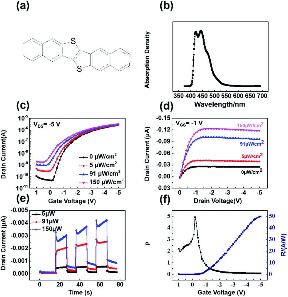 | ||
| Fig. 6 (a) Chemical structure of DNTT. (b) UV-vis absorption spectra of DNTT solution. (c) Photodetectors in the dark and different light intensities of 5 μW cm−2, 91 μW cm−2, 150 μW cm−2. (d) Output characteristics of DNTT photodetectors measured at different light intensities. (e) The photoresponse of the DNTT with the light switched “on” and “off” under given wavelength of 450 nm. (f) Photoresponsivity (R) and photocurrent/dark current ratio (P) of photodetectors based on DNTT. | ||
Conclusions
In conclusion, a stripping method has been developed to achieve smooth aluminum gate electrode. The roughness of stripped aluminum electrode is decreased dramatically to 0.9 nm compared with the value of 3.5 nm for as-deposited aluminum. After the aluminum gate electrode was potentiostatic anodized, the roughness of the alumina increased slightly. The bottom surface of the aluminum oxidized by potentiostatic anodization and then modified by n-ocadecyl phosphonic acid is an appropriate insulating layer with the leakage current density of about 10−7 A cm−2 at the voltage of −2 V, and the capacitance density of 0.114 μF cm−2. The DNTT OTFTs with the stripping AlOx anodized by potentiostatic anodization exhibit good charge transfer characteristics with a mobility of 0.53 cm2 V−1 s−1. OTFTs based on DNTT semiconductor shown photoresponsivity to the 450 nm blue light and can detect weak light intensity as low as 5 μW cm−2.Experimental
The procedure used for fabrication of the aluminum electrode
Silicon wafers and 2.5 mm thick PET films were cleaned in acetone, ethanol, de-ionized water, then dried on hot plate at 120 °C for 15 min. After treated with oxygen-plasma for 15 min, 10 mg mL−1 PS/chloroform solution was spin coated on the cleaned Si wafers at 5000 rpm. Aluminum film was evaporated on PS through a shadow mask. Then, UVAB coated PET films were covered on aluminum film, and solidified by irradiating 365 nm UV light for 5 min. The composite films were immersed in cyclohexane to dissolve PS. The buried aluminum on the surface of the UVAB adhered to PET films was peeled off from the Si wafers.Preparation of aluminum oxide and phosphonic acid self-assembled monolayers
The high-κ aluminum oxide gate dielectric layer was formed by potentiostatic anodization under ambient conditions (CHI660D electrochemical workstation, Shanghai Chen Hua Instrument Co., Ltd). A 0.0075 M citric acid monohydrate (C6H8O2·H2O) electrolyte was prepared with ultrapure water (18 MΩ cm). The contacted gates were immersed in the electrolyte to form the working electrode (anode), and platinum wire served as counter electrode, Ag/AgCl served as reference electrode. The aluminum film was then anodized with a constant voltage of 10 V for 10 min in a 0.0075 M citric acid monohydrate solution at 25 °C. The high-κ aluminum oxide gate dielectric layer was also can formed by oxygen-plasma treatment. The oxygen-plasma process was carried out for 30 min at 25 °C by UV-ozone treatment.Phosphonic acid self-assembled monolayers were prepared into solutions of 3 mM n-octadecyl phosphonic acid in isopropanol at room-temperature. The substrates were immersed in solution at room-temperature for 30 min, then rinsed with tetrahydrofuran followed by ethanol. Finally, these substrates were put on the hot plate at 100 °C to remove residual solvent.
Device fabrication
DNTT was then deposited onto substrates by thermal evaporation. Source and drain electrodes (W = 85 μm, L = 980 μm) were defined on top of the DNTT by evaporating a 50 nm-thick gold film through a shadow mask.Characterization
The morphologies of the aluminum electrode and were characterized by scanning electron microscopy (Hitachi SU8020) and atomic force microscopy (AFM) in tapping mode (Digital Instruments Multimode). The electrical characterization of the devices was measured by a Keithley 4200-SCS semiconductor parametric.Acknowledgements
We thank the National Natural Science Foundation of China (Grant No. 51573036) and the Program for New Century Excellent Talents in University (Grant No. NCET-12-0839).References
- (a) J. Sun, B. Zhang and H. E. Katz, Adv. Funct. Mater., 2011, 21, 29 CrossRef CAS; (b) S. Vasimalla, N. V. V. Subbarao and P. K. Iyer, J. Mater. Chem. C, 2016, 4, 7102 RSC; (c) Y. Xu, C. Liu, D. Khim and Y. Y. Noh, Phys. Chem. Chem. Phys., 2015, 17, 26553 RSC; (d) J. Lu, K.-S. Moon and C. P. Wong, in 12th International Symposium on Advanced Packaging Materials: Processes, Properties, and Interfaces, 2007, p. 187 Search PubMed; (e) H. Ma, H. L. Yip, F. Huang and A. K. Y. Jen, Adv. Funct. Mater., 2010, 20, 1371 CrossRef CAS; (f) T. H. Huang, K. C. Liu, Z. Pei, W. K. Lin and S. T. Chang, Org. Electron., 2011, 12, 1527 CrossRef CAS.
- (a) J. Reeder, M. Kaltenbrunner, T. Ware, D. Arreaga-Salas, A. Avendano-Bolivar, T. Yokota, Y. Inoue, M. Sekino, W. Voit, T. Sekitani and T. Someya, Adv. Mater., 2014, 26, 4967 CrossRef CAS PubMed; (b) U. Zschieschang, F. Ante, T. Yamamoto, K. Takimiya, H. Kuwabara, M. Ikeda, T. Sekitani, T. Someya, K. Kern and H. Klauk, Adv. Mater., 2010, 22, 982 CrossRef CAS PubMed; (c) U. Zschieschang, F. Ante, D. Kaelblein, T. Yamamoto, K. Takimiya, H. Kuwabara, M. Ikeda, T. Sekitani, T. Someya, J. Blochwitz-Nimoth and H. Klauk, Org. Electron., 2011, 12, 1370 CrossRef CAS.
- (a) P. F. Yu, W. Tang, L. R. Feng, J. Q. Zhao, Y. T. Li, Y. J. Liu and X. J. Guo, J. Disp. Technol., 2016, 12, 690 CrossRef; (b) T. Yokota, T. Sekitani, T. Tokuhara, N. Take, U. Zschieschang, H. Klauk, K. Takimiya, T. C. Huang, M. Takamiya, T. Sakurai and T. Someya, IEEE Trans. Electron Devices, 2012, 59, 3434 CrossRef.
- (a) J. Milvich, T. Zaki, M. Aghamohammadi, R. Rödel, U. Kraft, H. Klauk and J. N. Burghartz, Org. Electron., 2015, 20, 63 CrossRef CAS; (b) L. Zhang, T. Wu, Y. L. Guo, Y. Zhao, X. N. Sun, Y. G. Wen, G. Yu and Y. Q. Liu, Sci. Rep., 2013, 3, 1080 Search PubMed; (c) X. Liu, Y. Guo, Y. Ma, H. Chen, Z. Mao, H. Wang, G. Yu and Y. Liu, Adv. Mater., 2014, 26, 3631 CrossRef CAS PubMed.
- M. Zhu, S. Lv, Q. Wang, G. Zhang, H. B. Lu and L. Qiu, Nanoscale, 2016, 8, 7738 RSC.
- O. Acton, G. G. Ting, P. J. Shamberger, F. S. Ohuchi, H. Ma and A. K. Y. Jen, ACS Appl. Mater. Interfaces, 2010, 2, 511 CAS.
- L. A. Majewski, R. Schroeder, M. Grell, P. A. Glarvey and M. L. Turner, J. Appl. Phys., 2004, 96, 5781 CrossRef CAS.
- (a) F. Colleaux, J. M. Ball, P. H. Wobkenberg, P. J. Hotchkiss, S. R. Marder and T. D. Anthopoulos, Phys. Chem. Chem. Phys., 2011, 13, 14387 RSC; (b) N. Björklund, F. S. Pettersson, D. Tobjörk and R. Österbacka, Synth. Met., 2011, 161, 743 CrossRef; (c) H. Ma, O. Acton, D. O. Hutchins, N. Cernetic and A. K. Y. Jen, Phys. Chem. Chem. Phys., 2012, 14, 14110 RSC; (d) O. Acton, D. Hutchins, L. Arnadottir, T. Weidner, N. Cernetic, G. G. Ting, T. W. Kim, D. G. Castner, H. Ma and A. K. Y. Jen, Adv. Mater., 2011, 23, 1899 CrossRef CAS PubMed; (e) J. Collet, O. Tharaud, A. Chapoton and D. Vuillaume, Appl. Phys. Lett., 2000, 76, 1941 CrossRef CAS.
- (a) Q. Zhang, G. Xia, W. Xia, J. Zhou and S. Wang, Synth. Met., 2015, 210, 282 CrossRef CAS; (b) Y. M. Park, A. Desai, A. Salleo and L. Jimison, Chem. Mater., 2013, 25, 2571 CrossRef CAS; (c) L. A. Majewski, R. Schroeder and M. Grell, Adv. Funct. Mater., 2005, 15, 1017 CrossRef CAS; (d) J. D. Oh, J. W. Kim, D. K. Kim and J. H. Choi, Org. Electron., 2016, 30, 131 CrossRef CAS.
- (a) M. H. Yoon, H. Yan, A. Facchetti and T. J. Marks, J. Am. Chem. Soc., 2005, 127, 10388 CrossRef CAS PubMed; (b) M. E. Roberts, N. Queraltó, S. C. B. Mannsfeld, B. N. Reinecke, W. Knoll and Z. Bao, Chem. Mater., 2009, 21, 2292 CrossRef CAS; (c) W. Xu and S. W. Rhee, J. Mater. Chem., 2009, 19, 5250 RSC; (d) Y. G. Ha, S. Jeong, J. S. Wu, M. G. Kim, V. P. Dravid, A. Facchetti and T. J. Marks, J. Am. Chem. Soc., 2010, 132, 17426 CrossRef CAS PubMed; (e) C. Wang, W. Y. Lee, R. Nakajima, J. Mei, D. H. Kim and Z. Bao, Chem. Mater., 2013, 25, 4806 CrossRef CAS; (f) E. Reis Simas, E. S. H. Kang, A. Gassmann, E. Katholing and H. V. Seggern, J. Mater. Chem. C, 2015, 3, 9217 RSC; (g) S. Faraji, E. Danesh, D. J. Tate, M. L. Turner and L. A. Majewski, J. Phys. D: Appl. Phys., 2016, 49, 185102 CrossRef.
- (a) T. Uemura, M. Yamagishi, S. Ono and J. Takeya, Appl. Phys. Lett., 2009, 95, 103301 CrossRef; (b) S. Ono, K. Miwa, S. Seki and J. Takeya, Org. Electron., 2009, 10, 1579 CrossRef CAS; (c) T. Uemura, R. Hirahara, Y. Tominari, S. Ono, S. Seki and J. Takeya, Appl. Phys. Lett., 2008, 93, 263305 CrossRef; (d) S. Ono, S. Seki, R. Hirahara, Y. Tominari and J. Takeya, Appl. Phys. Lett., 2008, 92, 103313 CrossRef; (e) T. Uemura, M. Yamagishi, S. Ono and J. Takeya, Jpn. J. Appl. Phys., 2010, 49, 01AB13 CrossRef.
- (a) B. H. Lee, M. K. Ryu, S. Y. Choi, K. H. Lee, S. Im and M. M. Sung, J. Am. Chem. Soc., 2007, 129, 16034 CrossRef CAS PubMed; (b) K. S. Han, Y. Park, G. Han, B. H. Lee, K. H. Lee, D. H. Son, S. Im and M. M. Sung, J. Mater. Chem., 2012, 22, 19007 RSC; (c) K. Everaerts, J. D. Emery, D. Jariwala, H. J. Karmel, V. K. Sangwan, P. L. Prabhumirashi, M. L. Geier, J. J. McMorrow, M. J. Bedzyk, A. Facchetti, M. C. Hersam and T. J. Marks, J. Am. Chem. Soc., 2013, 135, 8926 CrossRef CAS PubMed; (d) Y. G. Ha, K. Everaerts, M. C. Hersam and T. J. Marks, Acc. Chem. Res., 2014, 47, 1019 CrossRef CAS PubMed; (e) V. K. Sangwan, D. Jariwala, K. Everaerts, J. J. McMorrow, J. T. He, M. Grayson, L. J. Lauhon, T. J. Marks and M. C. Hersam, Appl. Phys. Lett., 2014, 104, 083503 CrossRef.
- S. A. DiBenedetto, A. Facchetti, M. A. Ratner and T. J. Marks, Adv. Mater., 2009, 21, 1407 CrossRef CAS.
- A. Dey, A. Singh, A. Kalita, D. Das and P. K. Iyer, in India–Japan Expert Group Meeting on Biomolecular Electronics & Organic Nanotechnology for Environment Preservation, ed. A. Fujii, B. D. Malhotra, H. Kajii and S. Kumar, 2016, vol. 704 Search PubMed.
- M. Kaltenbrunner, T. Sekitani, J. Reeder, T. Yokota, K. Kuribara, T. Tokuhara, M. Drack, R. Schwödiauer, I. Graz, S. Bauer-Gogonea, S. Bauer and T. Someya, Nature, 2013, 499, 458 CrossRef CAS PubMed.
- (a) L. A. Majewski, R. Schroeder, M. Voigt and A. M. Grell, J. Phys. D: Appl. Phys., 2005, 870, 3367 Search PubMed; (b) C. Yang, K. Shin, S. Y. Yang, H. Jeon, D. Choi, D. S. Chung and C. E. Park, Appl. Phys. Lett., 2006, 89, 153508 CrossRef.
- S. Saito, K. Torii, Y. Shimamoto, S. Tsujikawa, H. Hamamura, O. Tonomura, T. Mine, D. Hisamoto, T. Onai, J. Yugami, M. Hiratani and S. Kimura, Appl. Phys. Lett., 2004, 84, 1395 CrossRef CAS.
- (a) T. Yamamoto and K. Takimiya, J. Am. Chem. Soc., 2007, 129, 2224 CrossRef CAS PubMed; (b) T. Yamamoto and K. Takimiya, J. Photopolym. Sci. Technol., 2007, 20, 57 CrossRef CAS.
- N. V. V. Subbarao, M. Gedda, S. Vasimalla, P. K. Iyer and D. K. Goswami, Phys. Status Solidi A, 2014, 211, 2403 CrossRef CAS.
- (a) A. I. Mardare, M. Kaltenbrunner, N. S. Sariciftci, S. Bauer and A. W. Hassel, Phys. Status Solidi A, 2012, 209, 813 CrossRef CAS; (b) K. Kang Dae and S. Chung Kun, Appl. Phys. Lett., 2006, 88, 233508 CrossRef.
- H. Klauk, U. Zschieschang, J. Pflaum and M. Halik, Nature, 2007, 445, 745 CrossRef CAS PubMed.
- M. S. Go, J. M. Song, C. Kim, J. Lee, J. Kim and M. J. Lee, Electron. Mater. Lett., 2015, 11, 252 CrossRef CAS.
- Q. H. Wang, M. Zhu, D. Wu, G. B. Zhang, X. H. Wang, H. B. Lu, X. H. Wang and L. Z. Qiu, J. Mater. Chem. C, 2015, 3, 10734 RSC.
| This journal is © The Royal Society of Chemistry 2017 |