
 Open Access Article
 This Open Access Article is licensed under a Creative Commons Attribution-Non Commercial 3.0 Unported Licence
Boosting the performance of resistive switching memory with a transparent ITO electrode using supercritical fluid nitridation
Cong Ye a,
Jia-Ji Wua,
Chih-Hung Panb,
Tsung-Ming Tsai*b,
Kuan-Chang Changcd,
Huaqiang Wud,
Ning Dengd and
He Qiand
a,
Jia-Ji Wua,
Chih-Hung Panb,
Tsung-Ming Tsai*b,
Kuan-Chang Changcd,
Huaqiang Wud,
Ning Dengd and
He Qiand
aFaculty of Physics and Electronic Science, Hubei University, State Key Laboratory on Integrated Optoelectronics, Jilin University Region, Wuhan 430062, China
bDepartment of Materials and Optoelectronic Science, National Sun Yat-Sen University, 70 Lien-hai Road, Kaohsiung, 804, Taiwan, Republic of China. E-mail: tmtsai@faculty.nsysu.edu.tw
cDepartment of Physics, National Sun Yat-Sen University, 70 Lien-hai Road, Kaohsiung, 804, Taiwan, Republic of China
dInstitute of Microelectronics, Tsinghua University, Beijing, China
First published on 15th February 2017
Abstract
A low temperature supercritical fluid nitridation (SCF-nitridation) technique was investigated to dope nitrogen into a indium-tin-oxide (ITO) electrode to boost the performance of hafnium oxide resistive random access memory (RRAM). After the SCF-nitridation treatment, the memory window for the N:ITO electrode device was increased from 40 to 100. Moreover, the operation voltages (VSET and VRESET) and currents (ION and IOFF) were remarkably decreased, in which the IOFF was decreased to 65 nA. The possible reason for the performance improvement of resistive switching memory with the ITO transparent electrode induced by SCF-nitridation treatment was carefully explored.
Introduction
Recently, due to its excellent characteristics, such as low power, high-speed operation and simple structure, resistive random access memory (RRAM) has been regarded as a promising candidate for next-generation non-volatile memory.1–6 In our previous research, a low temperature supercritical CO2 fluid (SCCO2) technique was proven to be an effective method to passivate and repair the defects in thin films as well as modify the dielectric properties and electrical performance of various thin film transistors (TFTs) and RRAM devices.7–9 The supercritical phase is peculiar for its characteristics of high penetration of gas and solubility of liquids. Normally, we introduce CO2 vapor into a high-pressure pump to form SCCO2, completing the phase change from vapor to supercritical fluid. Furthermore, by adding a small amount of ammonia (NH3·H2O) into the supercritical CO2 fluid, the NH3·H2O molecules can achieve supercritical fluid phase due to its phase being close to the ideal solution.In this study, we propose a novel nitrogen doping method and effectively doped nitrogen into an ITO electrode by adding a small amount of NH3·H2O into the SCCO2 fluid, which was called the SCF-nitridation technique. Concerning nitridation techniques, we have reported a post-annealing treatment of TiO2/HfO2 bilayer resistive accessory memory in an N2 atmosphere.10 Chen et al. also reported an NH3 treatment on a ITO/Hf:SiO2/TiN device.11 Both post-annealing under N2 atmosphere and treatment with a NH3 sputtering atmosphere are effective methods to realize an improvement in the performance in RRAM devices. In this experiment, due to the gas-level penetrability and liquid-level solubility of the supercritical fluid, the NH3·H2O molecules can be easily introduced into the ITO thin film at a low temperature (120 °C) and thus, doping nitrogen into an ITO electrode can be realized. Herein, we define low temperature as lower than 150 °C. To be a post-treatment technology, unlike post-annealing technology,10 the temperature is regarded as low temperature. To investigate the resistive switching properties of a RRAM device with a nitrogen doped ITO electrode, an ITO/HfO2/TiN device was fabricated and treated using the SCF-nitridation process. The effect of SCF-nitridation on the resistive switching behavior of the hafnium oxide film with ITO electrode was evaluated by the material and current conduction mechanism analyses. Finally, the reaction mechanism in RRAM with SCF-nitridation was also discussed to explain the reason for the performance improvement of hafnium oxide RRAM.
Experimental
The experimental specimens were prepared as follows: for both groups, HfO2 (15 nm) switching layers were deposited on a TiN/Ti/SiO2/Si substrate via magnetron sputtering with a HfO2 target at a RF power of 150 W. After HfO2 film deposition, a 70 nm ITO electrode was deposited on the HfO2 film to complete the ITO/HfO2/TiN sandwiched device. The sputtering process was executed under an argon atmosphere, at a sputtering rate of 30 standard-state cubic centimeters per minute (sccm) and a working pressure of 4 mTorr at room temperature. One group of the as-fabricated samples was placed into the reactive chamber of a SCF system. A simplified schematic of the SCF-nitridation process is shown in the inset of Fig. 1. Gaseous CO2 was transported from the cylinder to a high-pressure pump at a pressure of 3000 pounds per square inch (psi), completing the phase change from vapor to supercritical fluid. The samples were treated in the stainless steel chamber of the SCF system by SCCO2 fluid mixed with 0.5 mL of ammonia at 120 °C for one hour. The treatment temperature can be adjusted in the range of 85 °C to 150 °C, which is dependent on the experimental requirements. The electrical characteristics were recorded using an Agilent B1500 semiconductor parameter analyzer. | ||
| Fig. 1 The XPS spectra of In 3d5/2, O 1s, Sn 3d5/2 and N 1s, and the element molar fraction ratio of the ITO thin film. The inset shows a schematic diagram of the supercritical CO2 fluid (SCCF) nitridation process. | ||
Results and discussion
The film composition and chemical bonding states were investigated by X-ray photoelectron spectroscopy (XPS) of the pure ITO and SCF-nitrided ITO (N:ITO) electrodes. Fig. 1 shows the XPS survey spectrum of the N:ITO electrode, containing In 3d5/2, Sn 3d5/2, O 1s and N 1s peaks. By calculating the area proportion of each peak, we obtained the mole fraction ratio of each element in the N:ITO electrodes, in which the atomic ratio of In![[thin space (1/6-em)]](https://www.rsc.org/images/entities/char_2009.gif) :O:Sn:N = 38.8%:53.5%:4.3%:3.4%. In order to precisely clarify the nitrogen doping effect via SCF-nitridation, we divided the N 1s spectrum into three sub peaks by Gaussian fitting. The main peak was located at a binding energy of 400.7 eV corresponds to the N–O bond, and the other two peaks N–In and N–Sn were located at 397.8 eV and 396.3 eV, respectively.12–14 It can be inferred that nitrogen was doped into the ITO film and mainly exists as an N–O bond. When combined with the SCCF process mentioned above, a possible SCF-nitridation reaction related with the NH3·H2O molecule, which was carried into ITO electrode by the SCCO2 fluid was proposed and is shown schematically in Fig. 2. As the RRAM device with the ITO electrode was placed into the ammonia-mixed SCCO2 fluid environment, the H2O molecules were first removed by the molecular sieves present in the SCF system, while the NH3 molecules were carried into the ITO film. Generally, several dangling bonds exist in the grain boundary of ITO film, as shown in Fig. 2(a). From Fig. 2(b), it can be seen that the NH3 molecules, containing NH2− and H+, approach the grain boundary of the ITO film and a domination reaction occurs: NH2 + NH2 + NH2 → 2NH3↑ + N, as shown in Fig. 2(c). Finally, the N atoms mainly form the N–O bonds in the ITO film, which is consistent with the XPS results.
:O:Sn:N = 38.8%:53.5%:4.3%:3.4%. In order to precisely clarify the nitrogen doping effect via SCF-nitridation, we divided the N 1s spectrum into three sub peaks by Gaussian fitting. The main peak was located at a binding energy of 400.7 eV corresponds to the N–O bond, and the other two peaks N–In and N–Sn were located at 397.8 eV and 396.3 eV, respectively.12–14 It can be inferred that nitrogen was doped into the ITO film and mainly exists as an N–O bond. When combined with the SCCF process mentioned above, a possible SCF-nitridation reaction related with the NH3·H2O molecule, which was carried into ITO electrode by the SCCO2 fluid was proposed and is shown schematically in Fig. 2. As the RRAM device with the ITO electrode was placed into the ammonia-mixed SCCO2 fluid environment, the H2O molecules were first removed by the molecular sieves present in the SCF system, while the NH3 molecules were carried into the ITO film. Generally, several dangling bonds exist in the grain boundary of ITO film, as shown in Fig. 2(a). From Fig. 2(b), it can be seen that the NH3 molecules, containing NH2− and H+, approach the grain boundary of the ITO film and a domination reaction occurs: NH2 + NH2 + NH2 → 2NH3↑ + N, as shown in Fig. 2(c). Finally, the N atoms mainly form the N–O bonds in the ITO film, which is consistent with the XPS results.
 | ||
| Fig. 2 Schematic of the chemical reaction mechanism on the ITO film to illustrate the nitrogen doping effect via SCF-nitridation treatment. | ||
Fig. 3 presents the current–voltage (I–V) curve comparison for the RRAM devices with the pure ITO and N:ITO electrodes. During the electrical test, a voltage was applied on the TiN electrode when the ITO electrode was grounded. It can be seen that both samples show typical bipolar characteristics and a self-compliance current phenomenon occurs. The self-compliance phenomenon results from the ITO electrode and has been reported in our previous study.15,16 In addition, when comparing the RRAM device with a pure ITO electrode, the self-compliance current of the RRAM with a N:ITO electrode was slightly decreased from 110 μA to 80 μA. Moreover, after SCF-nitridation, the resistive switching (RS) parameters, including the operation current/voltage as well as the storage window (ON/OFF ratio, read at 0.1 V), were greatly improved. As observed from the inset of Fig. 3, the memory window for the N:ITO electrode device was enlarged from 40 to 100. Moreover, the operation voltages (VSET and VRESET) and currents (ION and IOFF) were remarkably decreased. It is worth noting that IOFF was decreased to 65 nA for the device with the N:ITO electrode. In addition, we compared the power consumption for both devices and it can be calculated that the power consumption was decreased to 120 nW for the device with the N:ITO electrode. As a result, lower power consumption as well as a larger storage window, which are beneficial to RRAM applications, can be achieved through SCF-nitridation.
 | ||
| Fig. 3 The typical I–V curves obtained for HfO2 RRAM with the pure ITO electrode and N:ITO electrode. The insets show the schematic structure of the device and the ON/OFF ratio with and without SCF-nitridation treatment. | ||
In order to further investigate the RS parameters of the RRAM devices with the pure ITO and N:ITO electrodes, we made the statistical distribution of RS parameters including the operation current/voltage, as shown Fig. 4(a and b). For the floating box charts, the top and bottom lines mean 90% and 10% distributions, and the box represents the 75–25% range. The 50% point is indicated by the lines inside the box. As can be seen in Fig. 4(a and b), from the length of an individual box, the RS parameters for the device with the N:ITO electrode show a small variation. This indicates that a higher uniformity was achieved for the RRAM device after the SCF-nitridation process.17–19 Moreover, when compared with the device with the ITO electrode, it was found from Fig. 4(a) that the average operation currents of ION and IOFF for the device with the N:ITO electrode were reduced by 50% and 70%, respectively. Moreover, the average operation voltages, including VSET and VRESET, were reduced by about 80% and 50%, respectively, as shown in Fig. 4(b). Fig. 4(c and d) show the reliability tests of the pulse endurance and retention for the RRAM device after the SCF-nitridation process. We found that the resistance ratio between the high resistive state (HRS) and the low resistive state (LRS) remains stable over 107 pulse cycle operations, as shown in Fig. 4(c). It has been reported that for the pure ITO electrode RRAM device, the pulse endurance was 104.16 Therefore, an excellent endurance was achieved for the N:ITO electrode RRAM device after the SCF-nitridation process. In addition, the retention characteristics have been presented in Fig. 4(d). The ON/OFF ratio can be kept for over 104 seconds at 85 °C, which indicates that the data storage capability is equal to a 10 year lifetime.20,21
 | ||
| Fig. 4 (a) The current distribution of LRS and HRS, and (b) voltage distribution of RESET and SET voltages for the ITO/HfO2/TiN and N:ITO/HfO2/TiN devices. (c) The endurance of the N:ITO/HfO2/TiN device shows the capability with standing continuous AC pulses over 107. (d) The retention properties of the N:ITO/HfO2/TiN device at 85 °C. | ||
To clarify the superiority of the N doping effect via SCF-nitridation, we further explored the possible switching mechanism for the RRAM device. From the current fitting results, shown in Fig. 5(a and b), it can be seen that the initial current conduction of HRS and LRS from 0 V to −0.08 V exhibited an ohmic conduction mechanism for both devices, which was caused by the intrinsic carriers of the ITO material.22 As the applied voltages become larger in range from −0.1 V to −0.25 V, the current conduction mechanism in the LRS was still dominated by the ohmic conduction mechanism for the device with the pure ITO electrode. However, for the device with the N:ITO electrode, the current conduction mechanism of the device in the LRS transferred to Schottky emission. This implies that the electrons have to surpass an additional potential energy barrier between the conductive filament (CF) and the N:ITO electrode.23,24
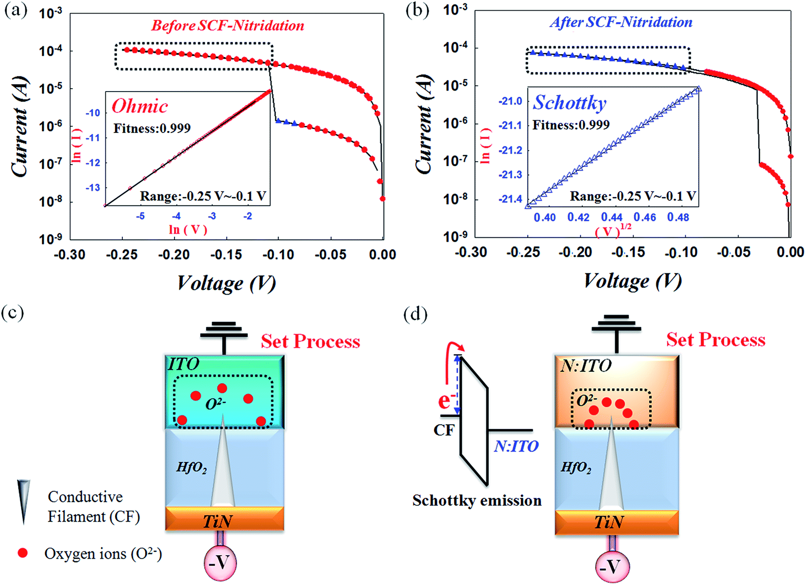 | ||
| Fig. 5 The conduction current fitting results of the RRAM devices with the (a) ITO/HfO2/TiN and (b) N:ITO/HfO2/TiN structures. A schematic of the migration of oxygen ions in the SET process with the (c) ITO/HfO2/TiN and (d) N:ITO/HfO2/TiN structures. | ||
According to the current fitting results, we further investigated the RS mechanisms for both devices to explore the possible reason for the performance improvement in the memory cell with the ITO transparent electrode induced by SCF-nitridation treatment. During the repeated set and reset process, the formation and rupture of CFs were accompanied by the recombination and separation of oxygen ions (O2−) and oxygen vacancies (Vo+) near by the ITO electrode.25 In the set process, for the pure ITO electrode,26 the O2− will transfer to the ITO electrode under the electrical force and a conductive filament (CF) was formed and connected to the ITO electrode as shown in Fig. 5(c). Therefore, the current conduction mechanism is dominated by the ohmic conduction in the LRS for the device with the pure ITO electrode. However, for the device with the N:ITO electrode, the N atom can capture and stop the oxygen atom to localize the oxygen near the CF tip.11,25 The bonding energy of the N–O bond is higher than that of the O–O bond,27,28 and therefore, the O2− ions prefer to form the N–O bond instead of participating in the reduction reaction. That is to say, the oxygen ions will concentrate around the CF tip during the SET process, as shown in Fig. 5(d). In contrast to Fig. 5(c), the oxygen ions are relatively scattered in the pure ITO electrode without the N atom. From Fig. 5(d), we assume that an oxygen-rich region was formed in the N:ITO electrode, which led to a Schottky barrier between the CF and the N:ITO electrode. Therefore, the current conduction mechanism for the device with the N:ITO electrode changed to Schottky emission, which was the main reason for the decrease in the LRS current, as shown in Fig. 4(a). In the reset process, for the device with the N:ITO electrode, an oxygen-rich region is formed in the N:ITO electrode, the oxygen ions are easier to repel from the N:ITO electrode under a lower reset voltage and the CF will be disconnected. Moreover, more oxygen ions participate in the oxidation reaction, which results in a longer distribution distance for the filament,15 and thus the HRS current was decreased to 65 nA. Therefore, when compared with the device before the SCF-nitridation treatment, a larger memory window as well as lower consumption power were obtained.
Conclusion
A low temperature supercritical fluid (SCF) nitridation technology was utilized to boost the performance of an RRAM device with ITO/HfO2/TiN structure. Nitrogen was successfully doped into the ITO electrode of the device after completing the fabrication of the RRAM device via a SCF-nitridation process. According to the XPS analyses and current fitting analyses, we found that an oxygen-rich region was formed around the conductive filament tip due to the nitrogen doping effect with N–O bond formation in the ITO electrode, which can be proven due to the fact that the current conduction mechanism is transferred to Schottky emission instead of ohmic conduction. The oxygen-rich region occurred in N:ITO and was a result of the SCF-nitridation process and can be regarded as the main reason for the decrease in the operation currents and the improvement in performance. We believe that the low-temperature SCF-nitridation technology is of great value for the performance improvement of RRAM devices in the future.Acknowledgements
This study was performed at the National Science Council Core Facilities Laboratory for Nano-Science and Nano-Technology in the Kaohsiung-Pingtung area. The study was partially supported by the National Natural Science Foundation of China (No. 61474039), the Natural Science Foundation (Key Project) of Hubei Province (No. 2015 CFA052), the Open Fund of State Key Laboratory on Integrated Optoelectronics (No. IOSKL2015KF14) and the Ministry of Science and Technology, Taiwan (MOST) under contract No. MOST-105-2221-E-110-025.Notes and references
- T. C. Chang, K. C. Chang, T. M. Tsai, T. J. Chu and S. M. Sze, Mater. Today, 2016, 19, 254–264 CrossRef CAS.
- S. Long, X. Lian, C. Cagli, X. Cartoixà, R. Rurali, E. Miranda, D. Jiménez, L. Perniola, M. Liu and J. Suñé, Appl. Phys. Lett., 2013, 102, 183505 CrossRef.
- C. Wang, H. Wu, B. Gao, L. Dai, N. Deng, D. Sekar, Z. Lu, M. Kellam, G. Bronner and H. Qian, IEEE Electron Device Lett., 2016, 37, 182–185 CrossRef CAS.
- T. C. Chang, F. Y. Jian, S. C. Chen and Y. T. Tsai, Mater. Today, 2011, 14, 608–615 CrossRef CAS.
- J. Sun, Q. Liu, H. Xie, X. Wu, F. Xu, T. Xu, S. Long, H. Lv, Y. Li and L. Sun, Appl. Phys. Lett., 2013, 102, 053502 CrossRef.
- Y. Zhang, N. Deng, H. Wu, Z. Yu, J. Zhang and H. Qian, Appl. Phys. Lett., 2014, 105, 063508 CrossRef.
- C. T. Tsai, P. T. Liu, T. C. Chang, C. W. Wang, P. Y. Yang and F. S. Yeh, IEEE Electron Device Lett., 2007, 28, 584–586 CrossRef CAS.
- K. C. Chang, T. M. Tsai, T. C. Chang, R. Zhang, K. H. Chen, J. H. Chen, M. C. Chen, H. C. Huang, W. Zhang and C. Y. Lin, IEEE Electron Device Lett., 2015, 36, 558–560 CrossRef CAS.
- H. L. Chen, T. C. Chang, T. F. Young, T. M. Tsai, K. C. Chang, R. Zhang, S. Y. Huang, K. H. Chen, J. Lou and M. C. Chen, Appl. Phys. Lett., 2014, 104, 243508 CrossRef.
- T. F. Deng, C. Ye, J. J Wu, P. He and H. Wang, Microelectron. Reliab., 2016, 57, 34 CrossRef CAS.
- J. Chen, K. C. Chang, T. C. Chang, T. M. Tsai, C. H. Pan, R. Zhang, J. C. Lou, T. J. Chu, C. H. Wu and M. C. Chen, IEEE Electron Device Lett., 2015, 36, 1138–1141 CrossRef CAS.
- H. Bonzel and G. Pirug, Surf. Sci., 1977, 62, 45–60 CrossRef CAS.
- J. Bian, X. Li, X. Gao, W. Yu and L. Chen, Appl. Phys. Lett., 2004, 84, 541–543 CrossRef CAS.
- Y. Inoue, M. Nomiya and O. Takai, Vacuum, 1998, 51, 673–676 CrossRef CAS.
- C. Ye, C. Zhan, T. M. Tsai, K. C. Chang, M. C. Chen, T. C. Chang, T. Deng and H. Wang, Appl. Phys. Express, 2014, 7, 034101 CrossRef.
- P. H. Chen, K. C. Chang, T. C. Chang, T. M. Tsai, C. H. Pan, C. Y. Lin, F. Y. Jin, M. C. Chen, H.-C. Huang and I. Lo, Appl. Phys. Express, 2016, 9, 034202 CrossRef.
- H. S. P. Wong, H. Y. Lee, S. Yu, Y. S. Chen, Y. Wu, P. S. Chen, B. Lee, F. T. Chen and M. J. Tsai, Proc. IEEE, 2012, 100, 1951–1970 CrossRef CAS.
- J. Lee, J. Shin, D. Lee, W. Lee, S. Jung, M. Jo, J. Park, K. P. Biju, S. Kim and S. Park, IEEE Int. Electron Devices Meet., 2010, 5–19 CAS.
- G. Wang, S. Long, Z. Yu, M. Zhang, T. Ye, Y. Li, D. Xu, H. Lv, Q. Liu and M. Wang, Appl. Phys. Lett., 2015, 106, 092103 CrossRef.
- C. Chen, S. Gao, G. Tang, C. Song, F. Zeng and F. Pan, IEEE Electron Device Lett., 2012, 33, 1711–1713 CrossRef CAS.
- J. Park, H. Jeon, H. Kim, W. Jang, H. Song, H. Kim, K. Lee and H. Jeon, RSC Adv., 2015, 5, 68900–68905 RSC.
- K. C. Chang, T. M. Tsai, T. C. Chang, Y. E. Syu, S. L. Chuang, C. H. Li, D. S. Gan and S. M. Sze, Electrochem. Solid-State Lett., 2011, 15, 65–68 CrossRef.
- P. H. Chen, K. C. Chang, T. C. Chang, T. M. Tsai, C. H. Pan, C. Y. Lin, F. Y. Jin, M. C. Chen, H. C. Huang and M. H. Wang, IEEE Electron Device Lett., 2016, 37, 584–587 CrossRef.
- C. Ye, T. Deng, J. Zhang, L. Shen, P. He, W. Wei and H. Wang, Semicond. Sci. Technol., 2016, 31, 105005 CrossRef.
- Y. E. Syu, R. Zhang, T. C. Chang, T. M. Tsai, K. C. Chang, J. C. Lou, T. F. Young, J. H. Chen, M. C. Chen and Y. L. Yang, IEEE Electron Device Lett., 2013, 34, 864–866 CrossRef CAS.
- P. H. Chen, K. C. Chang, T. C. Chang, T. M. Tsai, C. H. Pan, T. J. Chu, M. C. Chen, H. C. Huang, I. Lo, J. C. Zheng and S. M. Sze, IEEE Electron Device Lett., 2016, 37, 280–283 CrossRef CAS.
- K. P. C. Vollhardt and N. E. Schore, Organic Chemistry, Freeman, San Francisco, CA, USA, 3rd edn, 1998 Search PubMed.
- P. Atkins, Physical Chemistry, Oxford Univ. Press, New York, NY, USA, 8th edn, 2005 Search PubMed.
| This journal is © The Royal Society of Chemistry 2017 |