
 Open Access Article
 This Open Access Article is licensed under a Creative Commons Attribution-Non Commercial 3.0 Unported Licence
Understanding rectifying and nonlinear bipolar resistive switching characteristics in Ni/SiNx/p-Si memory devices
Sungjun Kim a,
Yao-Feng Changb and
Byung-Gook Park*a
a,
Yao-Feng Changb and
Byung-Gook Park*a
aDepartment of Electrical and Computer Engineering, Inter-University Semiconductor Research Center (ISRC), Seoul National University, Seoul 08826, South Korea. E-mail: bgpark@snu.ac.kr
bMicroelectronics Research Center, The University of Texas at Austin, Austin, Texas 78758, USA
First published on 23rd March 2017
Abstract
Two resistive memory devices were prepared with different doping concentrations in the silicon bottom electrodes to explore the self-rectifying and nonlinear resistive switching characteristics of Ni/SiNx/p-Si devices. Due to the reduced current overshoot effect, using electroforming at a positive bias can produce bipolar-type resistive switching behavior. A higher self-rectification ratio in the Ni/SiNx/p+-Si device is achieved than in the Ni/SiNx/p++-Si device. The asymmetric I–V characteristics can be explained by the Schottky barrier that suppresses the reverse current, and it is controllable by the size of the conducting path. A conducting path with a high resistance value in a low resistance state is beneficial for a high selection ratio. Moreover, by controlling the compliance current, we demonstrate an improved self-rectifying and selection ratio. The results of our experiment provide a possible way to improve the nonlinear characteristics without the need for a selector device in CMOS compatible cross-point array applications.
Introduction
Capacitance based memory technologies such as NAND flash, which has served as a leading player in the memory market, are expected to reach their physical limits soon, and new 3D structures are being introduced to further increase the memory density.1–4 Alternately, electrical resistance switch-based memory (RRAM) has attracted intense research interest as a promising candidate for use in next-generation non-volatile memory due to its high scalability down to a few nanometers and high-density integration with CMOS technology.5–22 Conventional devices consist of a metal–insulator–metal (MIM) structure, with insulator resistance switching caused by the diffusion of oxygen vacancies/defects, charge carrier trapping and de-trapping, and Schottky barrier modulation to produce the memory effect.5 Even though many dielectric materials such as HfOx (ref. 3) and TaOx,6 and non-stoichiometric SiOx (ref. 16 and 18) can be used as resistive switching materials, SiNx-based RRAM also shows good resistive switching performance in terms of its operating power, switching speed, and reliability.23–30Meanwhile, a device composed of a metal–insulator–silicon (MIS) structure is more flexible in terms of its resistive switching properties.23–37 Nano-structures with a tapered sidewall profile, which is favourable for the electric field concentration, can be made via anisotropic wet etching of a silicon surface.25 Also, the work function of the silicon surface acting as a bottom electrode is easily tuned by controlling the impurity concentration, leading to a difference in the resistive switching observed for a low-dopant concentration in silicon surface.29 Diode-like resistive switching would be one of the most significant advantages of the high-density crossbar array.
Rectifying and nonlinear characteristics are a quite important requirement for two-terminal based emerging memories such as RRAM and phase change RAM (PRAM) employing a cross-point array due to sneak path issues.38–43 Several architectures have been proposed to solve this issue, such as one diode and one resistive switching element connection (1D-1R),39 one transistor and one resistive switching element connection (1T-1R)40 or one selector and one resistive switching element connection (1S-1R).41 However, considering the design specifications and integration availability, a select-less resistive switching element can ease the design and material complexity due to the inherent rectifying and nonlinear properties of the simple unit device.
Current overshoot is an important issue for RRAM commercialization.44–46 It is easily confirmed by the fact that the reset current is much higher than the ICC that is applied using external equipment. The ICC independent current overshoot is contributed by parasitic capacitance in a device as well as the testing equipment including a cable and probe station. Integrated 1T-1R can solve the issue, but it is not suitable for high-density memory. Hence, uncontrollable conducting path growth and a high reset power consumption, which can be caused by an overshoot current, hinders RRAM commercialization due to its high power consumption.
So far, RRAM devices with an MIS structure have been reported in the literature.25–37 In a recent study, we reported on self-rectifying unipolar resistive switching in SiNx-based RRAM.27 For unipolar switching, it is difficult to perform uniform and repetitive resistive switching due to the narrow margin between the set voltage and the reset voltage. On the other hand, bipolar switching, in which a different polarity is used for set and reset switching, is more favourable to high performance applications as long as the leakage current elements can be suppressed in a cross-point array. In this work, we investigate the current overshoot effects and the successful resistive switching current range, depending on the bias polarity and dopant concentration in the silicon bottom electrode surface.
Experimental
To form the bottom electrode in an MIS system, difluoroboron (BF2) ions were implanted with an energy of 40 keV into a single crystalline Si substrate. The doses of p+ Si and p++ Si in the bottom electrodes were 5 × 10¹³ and 5 × 1015 cm−2, respectively. The lattice damage was repaired, and the dopants were activated by the drive-in process at 1050 °C for 10 min. A 4 nm thickness SiNx film, serving as a resistive switching layer, was then deposited using low-pressure chemical vapor deposition (LPCVD) at 785 °C, with a mixture of SiH2Cl2 (30 sccm) and NH3 (100 sccm). Finally, the Ni top electrode was deposited using a thermal evaporator using a shadow mask, with a device size of 100 μm. All electrical properties were characterized via the DC voltage sweep mode and the pulse mode using a Keithley 4200-SCS semiconductor parameter analyzer and a 4225-PMU ultra-fast current–voltage (I–V) module at room temperature, respectively. To operate the device, the bottom electrodes of the p+ Si and p++ Si surfaces were grounded, and a bias voltage was applied on the Ni top electrode. To analyze the SiNx material deposited in our laboratory using different methods, X-ray photoelectron spectroscopy (XPS) analysis was performed using a Thermo VG ESCA Sigma Probe spectrometer operating at 15 kV and 100 W with a monochromatic Al-Ka radiation source. The calibration of the binding energy scale was set by fixing the C 1s at 284.5 eV.Results and discussion
Fig. 1(a) and (b) show high-resolution XPS of the Si 2p and N 1s spectra for the SiNx film, respectively.47 The atomic concentration was calculated from Si 2p and the N 1s peaks. The N/Si ratio in the SiNx was 0.87. When compared to the stoichiometric Si3N4 sample (x = 1.33), our silicon-rich SiNx sample (x < 1.33) offers favorable resistive switching behavior due to the higher density of traps in the SiNx film. Fig. 2(a) shows typical bipolar I–V curves of the Ni/SiNx/p++ Si device and Ni/SiNx/p+ Si device for electroforming at a positive voltage. A compliance current (ICC) of 300 μA was applied to the devices to limit the size of the conducting path, and a higher low-resistance-state (LRS) current was observed for the Ni/SiNx/p++ Si device compared to the Ni/SiNx/p+ Si device since the current overshoot can affect the size of the conducting path in the SiNx film.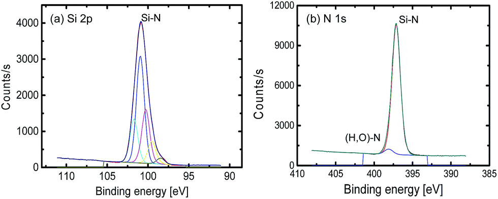 | ||
| Fig. 1 XPS spectra of the SiNx film deposited via LPCVD: (a) Si 2p and (b) N 1s. | ||
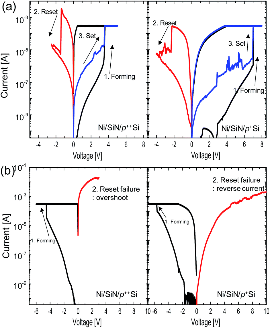 | ||
| Fig. 2 (a) Typical I–V curves of the Ni/SiNx/p++ Si device (left) and Ni/SiNx/p+ Si device (right); electroforming at (a) positive voltage, and (b) negative voltage. | ||
The subsequent LRS current after the forming and set process is a good barometer of the current overshoot. For the reset process, the devices are switched from LRS to a high-resistance-state (HRS) when a negative bias is applied to the devices. An additional current surge is observed for the Ni/SiNx/p++ Si device before a sharp current drop. The positive bias leads to set switching, in which the devices are switched from HRS to LRS. Here, for both devices, the forming-free resistive switching makes no difference between the forming and the set voltage due to the thinness of the SiNx layer.48 Unlike most metal oxide-based RRAM that use the movement of oxygen vacancies, the switching mechanism in SiN-based RRAM is still unclear. We believe that the switching mechanism of the SiN-based RRAM is basically related to the traps in the SiN film that can be affected by the deposition methods and subsequent switching. The formation and rupture of conducting paths made up of many traps from dangling bonds in the trivalent Si atoms can lead to resistive switching.24 Much more than the amount of initial traps are required for an effective conducting path for the set process and the accelerated electrons with a thermal effect under a high electric field trigger bonding breakage in the SiN film. Then, the electrons injected through the increased trap sites can produce additional traps again. Recently, X. Jiang et al., reported that hydrogen can play an important role in resistive switching, including the reset process.28
Fig. 2(b) shows typical bipolar I–V curves of the Ni/SiNx/p++ Si device and Ni/SiNx/p+ Si device for electroforming at a negative voltage with a compliance current of 300 μA. Note that low reset switching yields were observed for both devices under the negative forming process. For the Ni/SiNx/p++ Si device, a severe current overshoot leads to a very large conducting path that is hard to rupture, even at a high reset power. On the other hand, for the Ni/SiNx/p+ Si, the reset failure indicates that the reverse current suppressed by the Schottky barrier is not appropriate to rupture the conducting path. The suppressed current may have a negative effect on the reset switching driven by Joule heating and field enhancement. To further identify the current overshoot effect, Fig. 3(a–d) show a check of the distribution of the LRS resistance (RLRS) as a function of the ICC after a positive and a negative forming of the Ni/SiNx/p++ Si and Ni/SiNx/p+ Si devices.
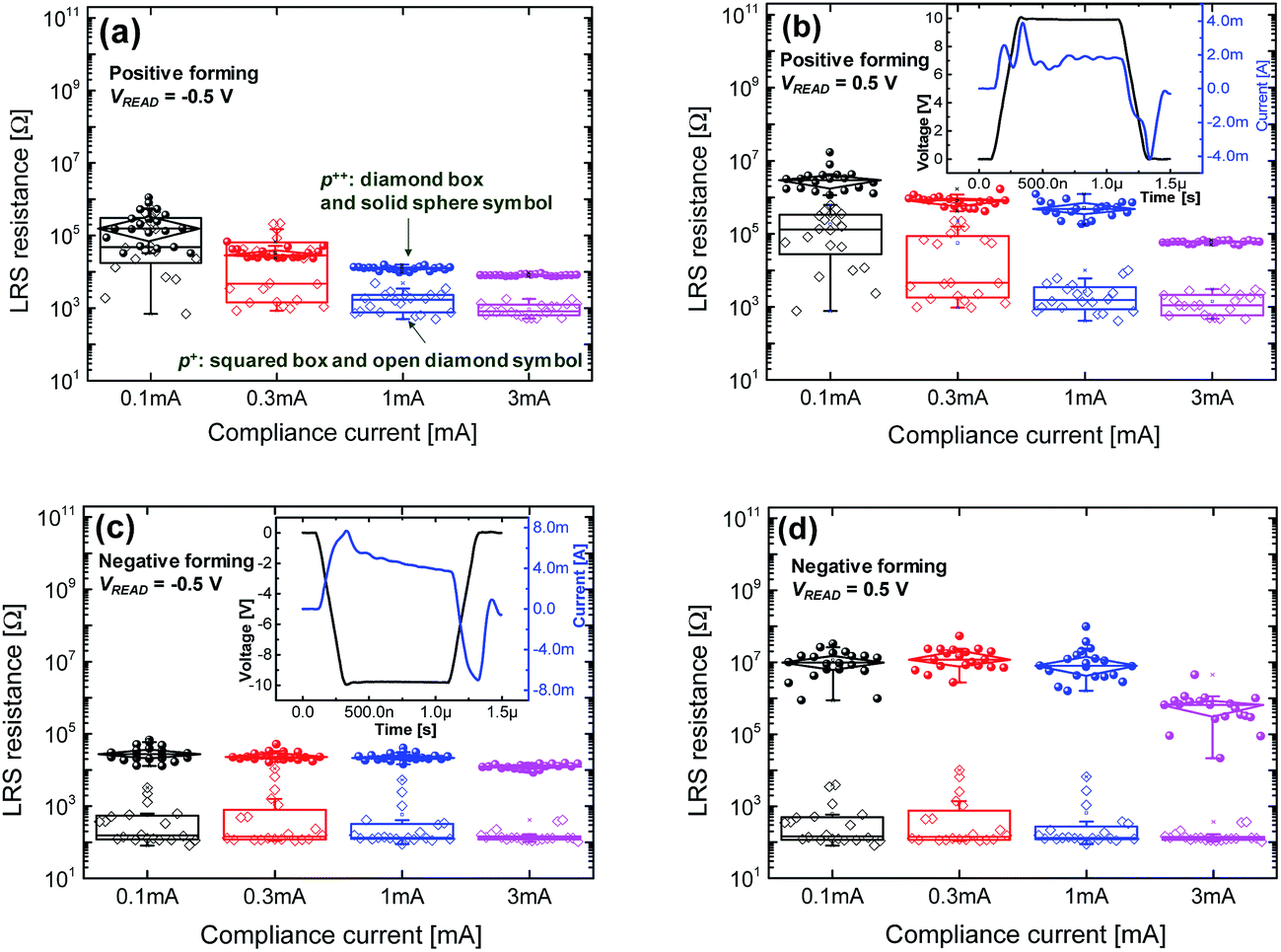 | ||
| Fig. 3 (a) Statistical distribution of the LRS resistance for the Ni/SiNx/p++ Si device and Ni/SiNx/p+ Si device: read voltage of −0.5 V (a), and 0.5 V (b) for positive forming; and read voltage of −0.5 V (c), and 0.5 V (d) for negative forming. The insets of (b) and (c) show the transient characteristics of positive forming and negative forming, respectively, for the Ni/SiNx/p+ Si device. | ||
When we read HRS and LRS, we do not setup the compliance current for read operation. Low read voltage of ±0.5 V cannot affect subsequent resistive switching by read disturbance. After the positive forming, the RLRS value in both devices decreases with the ICC. Note that a low RLRS is randomly observed for the Ni/SiNx/p++ Si device, even though a low ICC is imposed to the device for low-power switching, leading to poor controllability of the conducting path. The current overshoot leads to very high current in the LRS, which can have a tail bit in distribution for Ni/SiNx/p++ Si structure. Conversely, the Ni/SiNx/p+ Si device has a much higher RLRS with better uniformity. Also, note that Fig. 3(a) and (b) show that the RLRS at a positive region is higher than that at a negative region. When negative forming is used for the Ni/SiNx/p++ Si device, a more severe current overshoot is observed, leading to very low RLRS with a large conducting path, regardless of the polarity of the read voltage, as shown in Fig. 3(c) and (d), indicating that there is a very weak rectifying effect.
The insets in Fig. 3(b) and (c) show the transient characteristics of positive forming and negative forming, respectively, for the Ni/SiNx/p+ Si device. A single pulse with a height of 10 and −10 V is applied to the device for positive forming and negative forming, respectively. The peak current that indicates the overshoot current in negative forming is higher than that in positive forming.
Tunneling carriers from the metal electrode and the silicon bottom electrode may affect the current overshoot. For positive forming, the electrons and holes are injected from a silicon electrode and Ni electrode, respectively. For negative forming, the injections of the carriers are in the opposite direction, leading to a much higher overshoot due to the abundant carrier concentrations. Note that, except for a reverse current suppressed by the Schottky barrier, which is not appropriate to rupture the conducting path, the polarity effect induced by the resistive switching behavior can be potentially explained by the filament tip contact location in the localized region (close to Ni top electrode or p+ Si bottom electrode).49 Further studies in the conducting path growth direction and rupture mechanism during the switching process will be challenging, but it is important to have robust device performance prediction in compact model analysis.
Fig. 4(a) shows the energy band diagrams of the Ni/SiNx/p+ Si device under the reverse bias considering the material properties. At a low voltage bias region (0.05–1 V), the holes from the Ni top electrode tunnel into the trap state in the SiNx layer that can be controlled by the ICC, and then the hole injection from SiNx layer to p+ Si is strongly affected by the depletion region in the p-Si surface. Unlike the Ni/SiNx/p++ Si device, the depletion region from a lower dopant concentration in the silicon surface acting as the series resistance helps alleviate the current overshoot. More importantly, the Schottky barrier that formed at the surface of the silicon bottom electrode is responsible for the asymmetric I–V curves. The forward current and reverse current are driven by a negative bias voltage and a positive bias voltage, respectively. The forward bias voltage lowers the energy barrier in the depletion region, causing the carriers to move fluently. The forward current (IF) can be expressed as IF = IR{exp(eV/nkBT) × 1}, where IR is the reverse current IR = A*AT2![[thin space (1/6-em)]](https://www.rsc.org/images/entities/char_2009.gif) exp(−ØB/kBT), n is the ideality factor, kB is the Boltzmann constant, T is the Kelvin temperature, A* is the effective Richardson constant, A is the contact area, and ØB is the Schottky barrier height. The Schottky barrier suppresses the reverse current, considering ØB is bias voltage-independent.
exp(−ØB/kBT), n is the ideality factor, kB is the Boltzmann constant, T is the Kelvin temperature, A* is the effective Richardson constant, A is the contact area, and ØB is the Schottky barrier height. The Schottky barrier suppresses the reverse current, considering ØB is bias voltage-independent.
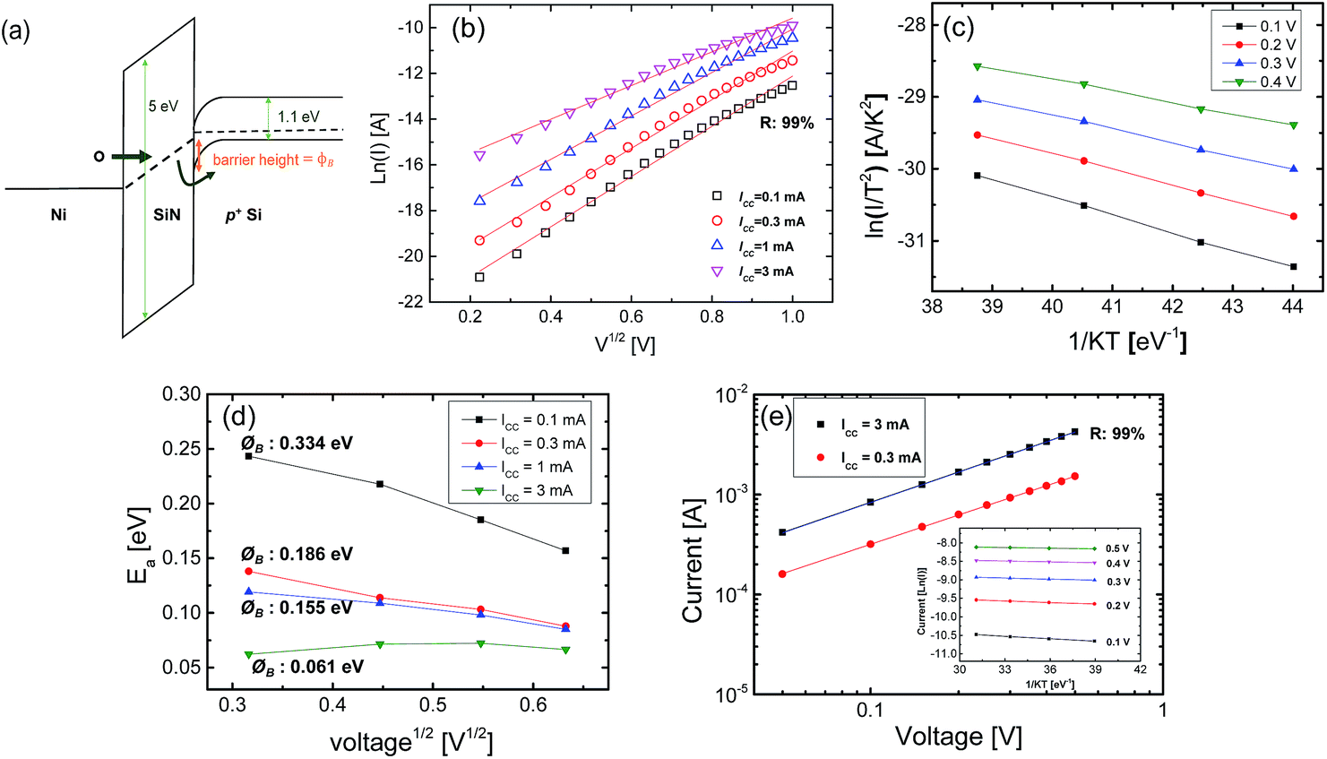 | ||
| Fig. 4 (a) Energy band diagram of the Ni/SiNx/p+ Si device under a negative bias. (b) ln(I) versus V1/2 plots with different compliance currents for Ni/SiNx/p+ Si device under negative bias. (c) Plot of ln(I/T2) vs. 1/kT at 0.1, 0.2, 0.3, and 0.4 V for Ni/SiNx/p+ Si device. (d) Plot of Ea vs. V1/2 for Ni/SiNx/p+ Si device. (e) log–log plot and temperature dependence of Ni/SiNx/p++ Si device. | ||
It is also confirmed that all reverse currents of the Ni/SiNx/p+ Si device in the LRS caused by different ICC (0.1, 0.3, 1, and 3 mA) are well fitted with the I–V relationship of ln(I) ∼ V1/2, as shown in Fig. 4(b), indicating the reverse current is dominated by Schottky emission. Fig. 4(c) shows a plot of ln(I/T2) versus 1/kT for ICC of 0.3 mA. The slope of Fig. 4(c) means the activation energy (Ea) at the bias voltages (0.1–0.4 V), and then a ØB can be extracted from the plot of Ea versus V1/2 in Fig. 4(d).
The ØB is reduced with increasing ICC, indicating that the ØB can be modulated by the size of the conducting path, which is better controllable through ICC for the Ni/SiNx/p+ Si device. Fig. 4(e) shows the log–log plot of the reverse current of the Ni/SiNx/p++ Si device. Unlike the Ni/SiNx/p+ Si device, the Ni/SiNx/p++ Si device shows ohmic conduction for the reverse current, suggesting strong and continuous conducting paths are formed within the SiNx film. The inset of Fig. 4(e) shows that the current slightly increased with the temperature, indicating that the conducting path has semiconducting properties.
We define two crucial parameters to assess the nonlinearity of the LRS current. The first parameter is the forward-to-reverse current ratio (F/R ratio) that is important for bipolar switching as well as unipolar switching, as shown in Fig. 5(a). The forward current can be affected by the thickness of the SiNx film and the size of the conducting path. The reverse current can be mainly determined by the Schottky barrier, as seen by the holes. Fig. 5(b) shows the F/R ratio as a function of the ICC for both devices. The Ni/SiNx/p++ Si device has a very low F/R ratio regardless of the ICC, suggesting that the interface resistance and barrier between the SiNx layer and p++ Si are negligible due to the degenerated Si surface with a high dopant concentration. Therefore, the carriers move freely without encumbrance of the barrier, and then the size of the conducting path cannot affect the F/R ratio.
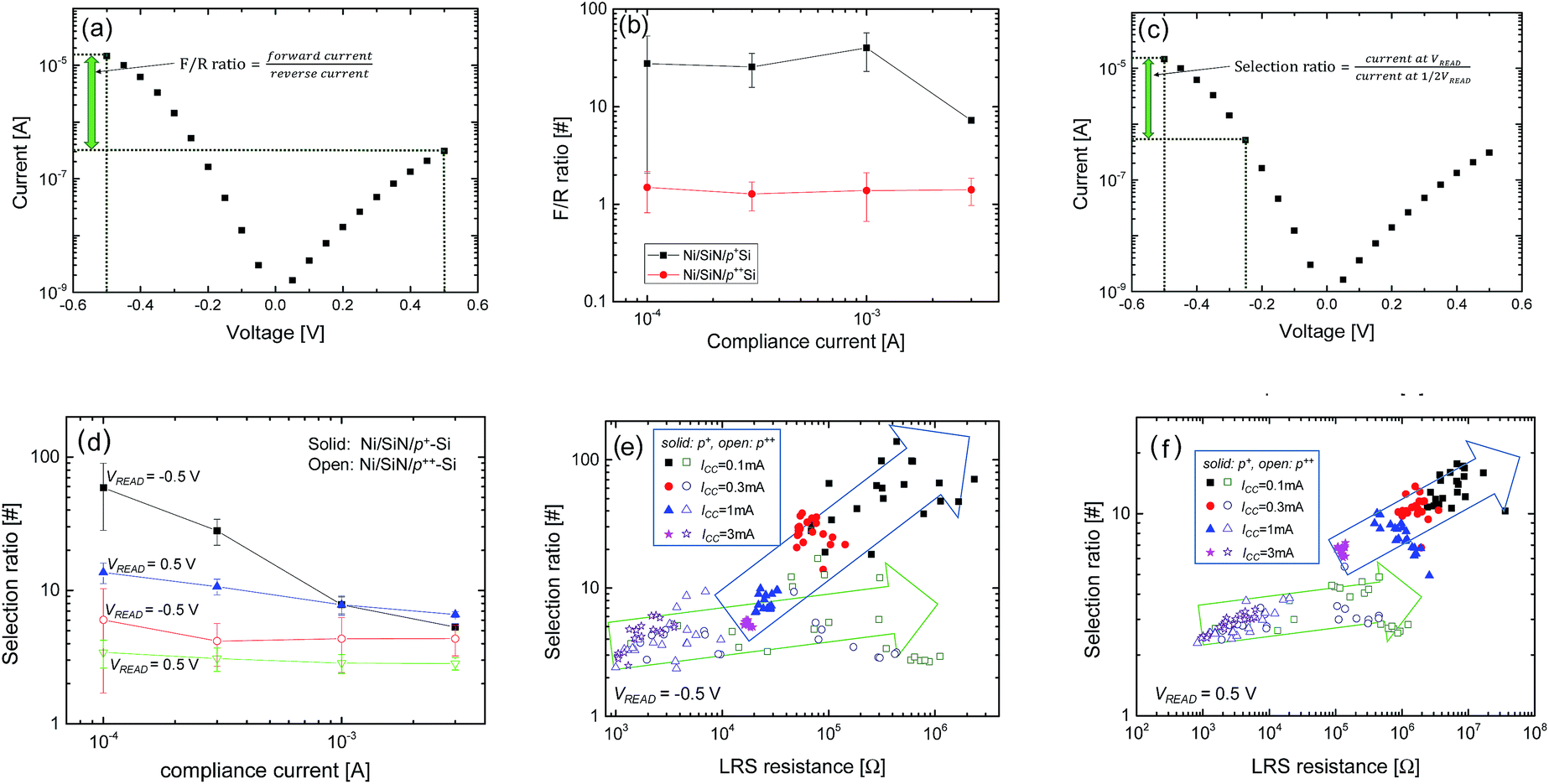 | ||
| Fig. 5 (a) I–V characteristics in the low voltage region in a Ni/SiNx/p+ Si device for F/R ratio. (b) F/R ratio as a function of the compliance current for the Ni/SiNx/p+ Si device and the Ni/SiNx/p++ Si device. (c) I–V characteristics in the low voltage region in Ni/SiNx/p+ Si device for selection ratio. (d) Selection ratio as a function of the compliance current. Selection ratio-LRS resistance scatter plots for nonlinearity at a read voltage of −0.5 V (e), and 0.5 V (f). | ||
On the other hand, a much higher F/R ratio in the Ni/SiNx/p+ Si device is obtained compared to the Ni/SiNx/p++ Si device. For the ICC of 3 mA, the main cause of the reduced F/R ratio would be attributed to a shape increase in the reverse current since the conducting path is too large with a loss of Schottky barrier transport, indicating that the size of the conducting path can modulate the Schottky barrier. The second important parameter for the nonlinear characteristics is the selection ratio (SR) that can be defined as SR = I@VREAD/I@0.5VREAD, as shown in Fig. 5(c). A read voltage that is as low as possible is desirable to minimize the read disturbance, and it causes less stress in the device cells. Fig. 5(d) show the SR at a VREAD of ±0.5 V as a function of the ICC for both devices, and much higher nonlinear I–V characteristics in the Ni/SiNx/p+ Si device are observed, compared to the Ni/SiNx/p++ Si device.
Fig. 5(e) and (f) show the SR versus the LRS resistance of the forward and reverse bias, respectively, for both devices. For the Ni/SiNx/p++ Si device, the inherent weak nonlinearity is related to the conducting path with semiconducting behavior. Unlike metal nitride-based RRAM devices showing metallic properties of the conducting filaments in the LRS, the intrinsic SiNx-based RRAM device shows non-ohmic I–V characteristics when even a large conducting path is formed in the SiNx film.50–53 Moreover as the LRS resistance increases, the selection ratio tends to increase, as shown in Fig. 5(e) and (f). The experimental results are consistent with the theoretical background of the conduction transport in the conducting path with quantum-size effects.54,55
In particular, the Ni/SiNx/p+ Si device that has a well-controlled conducting path by the ICC shows a clearer relationship between the SR and LRS resistance. The maximum value is higher than 100 for the forward current when the conducting path with LRS resistance of more than 100 kΩ is formed. The narrow conducting path with a high LRS resistance induced by a low ICC can boost the SR, without an additional selection device. Note that the SR in the forward current is much higher than that in the reverse current. As previously mentioned, the forward current is sensitive to changes in the applied bias voltage. Therefore, for forward current, tunneling transport governed by trap-assisted-tunneling (TAT) and conducting path in the SiNx film plays an important role in the nonlinear characteristics.10,56–58 On the other hand, in a low voltage region, the reverse current suppressed by the Schottky barrier height shows weaker nonlinear characteristics.
Conclusions
In summary, the Ni/SiNx/p+-Si device shows better rectifying and nonlinear bipolar resistive switching behavior when compared to the Ni/SiNx/p++-Si device. The electroforming process at a positive voltage guarantees better resistive switching performance due to the reduced current overshoot. The rectifying I–V characteristic is attributed to the Schottky barrier in the silicon surface that suppresses the reverse current. Since the conducting path that can be controlled by the ICC shrinks, the selection ratio generally increases, which shows great potential to produce high-density memory in a cross-point array.Acknowledgements
This work was supported by a grant from the National Research Foundation of Korea (NRF), funded by the Korean government (MSIP) (2015R1A2A1A01007307).Notes and references
- Y. Kim, M. Kang, S. H. Park and B.-G. Park, IEEE Electron Device Lett., 2013, 34, 990–992 CrossRef CAS.
- J. H. Yoon, S. Yoo, S. J. Song, K. J. Yoon, D. E. Kwon, Y. J. Kwon, T. H. Park, H. J. Kim, X. L. Shao, Y. Kim and C. S. Hwang, ACS Appl. Mater. Interfaces, 2016, 8, 18215–18221 CAS.
- S. Yu, H.-Y. Chen, B. Gao, J. Kang and H. S. Philip Wong, ACS Nano, 2013, 7, 2320–2325 CrossRef CAS PubMed.
- Q. Luo, X. Xu, H. Liu, H. Lv, T. Gong, S. Long, Q. Liu, H. Sun, W. Banerjee, L. Li, J. Gao, N. Lu and M. Liu, Nanoscale, 2016, 8, 15629–15636 RSC.
- R. Waser, R. Dittmann, G. Staikov and K. Szot, Adv. Mater., 2009, 21, 2632–2663 CrossRef CAS.
- M.-J. Lee, C. B. Lee, D. Lee, S. R. Lee, M. Chang, J. H. Hur, Y.-B. Kim, C.-J. Kim, D. H. Seo and S. Seo, Nat. Mater., 2011, 10, 625–630 CrossRef CAS PubMed.
- E. Linn, R. Rosezin, C. Kügeler and R. Waser, Nat. Mater., 2010, 9, 403–406 CrossRef CAS PubMed.
- L. Goux, N. Raghavan, A. Fantini, R. Nigon, S. Strangio, R. Degraeve, G. Kar, Y. Y. Chen, F. De Stefano and V. Afanas, J. Appl. Phys., 2014, 116, 134502 CrossRef.
- L. Zhao, H.-Y. Chen, S.-C. Wu, Z. Jiang, S. Yu, T.-H. Hou, H.-S. Philip Wong and Y. Nishi, Nanoscale, 2014, 6, 5698–5702 RSC.
- Y.-F. Chang, B. Fowler, Y.-C. Chen and J. C. Lee, Prog. Solid State Chem., 2016, 44, 75–85 CrossRef CAS.
- B. Fowler, Y.-F. Chang, F. Zhou, Y. Wang, P.-Y. Chen, F. Xue, Y.-T. Chen, B. Bringhurst, S. Pozder and J. C. Lee, RSC Adv., 2015, 5, 21215–21236 RSC.
- Q. Li, Y. Li, L. Gao, F. Ma, Z. Song and K. Xu, RSC Adv., 2016, 6, 42347–42352 RSC.
- H. Zhang, L. Liu, B. Gao, Y. Qiu, X. Liu, J. Lu, R. Han, J. Kang and B. Yu, Appl. Phys. Lett., 2011, 98, 042105 CrossRef.
- T.-L. Tsai, Y.-H. Lin and T.-Y. Tseng, IEEE Electron Device Lett., 2015, 36, 675–677 CrossRef CAS.
- K. C. Chang, T. C. Chang, T. M. Tsai, R. Zhang, Y. C. Hung, Y. E. Syu, Y. F. Chang, M. C. Chen, T. J. Chu, H. L. Chen, C. H. Pan, C. C. Shih, J. C. Zheng and S. M. Sze, Nanoscale Res. Lett., 2016, 10, 120 CrossRef PubMed.
- Y.-C. Chen, Y.-F. Chang, X. Wu, F. Zhou, M. Guo, C.-Y. Lin, C.-C. Hsieh, B. Fowler, T.-C. Chang and J. C. Lee, RSC Adv., 2017, 7, 12984 RSC.
- H. Lv, Y. Li, Q. Liu, S. Long, L. Li and M. Liu, IEEE Electron Device Lett., 2015, 36, 675–677 CrossRef.
- F. Zhou, Y.-F. Chang, B. Fowler, K. Byun and J. C. Lee, Appl. Phys. Lett., 2015, 106, 063508 CrossRef.
- A. Prakash, D. Deleruyelle, J. Song, M. Bocquet and H. Hwang, Appl. Phys. Lett., 2015, 106, 233104 CrossRef.
- Z. Wang, J. Kang, Z. Yu, Y. Fang, Y. Ling, Y. Cai, R. Huang and Y. Wang, Nanotechnology, 2017, 28, 055204 CrossRef PubMed.
- Y.-C. Shin, T.-H. Wang, J.-S. Huang, C.-C. Lai, Y.-J. Hong and Y.-L. Chueh, RSC Adv., 2016, 6, 61221 RSC.
- S. Kim, S. Choi, J. Lee and W. D. Lu, ACS Nano, 2014, 8, 10262–10269 CrossRef CAS PubMed.
- H.-D. Kim, H.-M. An, S. M. Hong and T. G. Kim, Phys. Status Solidi A, 2013, 210, 1822 CAS.
- J. H. Park, H.-D. Kim, S. M. Hong, M. J. Yun, D. S. Jeon and T. G. Kim, Phys. Status Solidi RRL, 2014, 8, 239 CrossRef CAS.
- S. Kim, S. Jung, M.-H. Kim, T.-H. Kim, S. Bang, S. Cho and B.-G. Park, Nanotechnology, 2017, 28, 125207 CrossRef PubMed.
- S. Kim, S. Jung, M.-H. Kim, S. Cho and B.-G. Park, Appl. Phys. Lett., 2015, 106, 222106 Search PubMed.
- S. Kim, S. Cho and B.-G. Park, AIP Adv., 2016, 6, 015021 CrossRef.
- X. Jiang, Z. Ma, J. Xu, K. Chen, L. Xu, W. Li, X. Huang and D. Feng, Sci. Rep., 2015, 5, 15762 CrossRef CAS PubMed.
- Y. T. Chen, B. Fowler, Y. Wang, F. Xue, F. Zhou, Y. F. Chang, P. Y. Chen and J. C. Lee, IEEE Electron Device Lett., 2012, 33, 1702 CrossRef CAS.
- Y. F. Chang, L. Ji, Y. Wang, P. Y. Chen, F. Zhou, F. Xue, B. Fowler, E. T. Yu and J. C. Lee, Appl. Phys. Lett., 2013, 103, 193508 CrossRef.
- Y.-F. Chang, B. Fowler, Y.-C. Chen, Y.-T. Chen, Y. Wang, F. Xue, F. Zhou and J. C. Lee, J. Appl. Phys., 2014, 116, 043708 CrossRef.
- Y.-F. Chang, B. Fowler, Y.-C. Chen, Y.-T. Chen, Y. Wang, F. Xue, F. Zhou and J. C. Lee, J. Appl. Phys., 2014, 116, 043709 CrossRef.
- Y. F. Chang, L. Ji, Z. J. Wu, F. Zhou, Y. Wang, F. Xue, B. Fowler, E. T. Yu, P. S. Ho and J. C. Lee, Appl. Phys. Lett., 2013, 103, 033521 CrossRef.
- Y. F. Chang, P. Y. Chen, B. Fowler, Y. T. Chen, F. Xue, Y. Wang, F. Zhou and J. C. Lee, J. Appl. Phys., 2012, 112, 123702 CrossRef.
- F. Zhou, Y. F. Chang, Y. Wang, Y. T. Chen, F. Xue, B. W. Fowler and J. C. Lee, Appl. Phys. Lett., 2014, 105, 163506 CrossRef.
- S. Gao, F. Zeng, F. Li, M. Wang, H. Mao, G. Wang, C. Song and F. Pan, Nanoscale, 2015, 7, 6031–6038 RSC.
- Y. F. Chang, P. Y. Chen, Y. T. Chen, F. Xue, Y. Wang, F. Zhou, B. Fowler and J. C. Lee, Appl. Phys. Lett., 2012, 101, 052111 CrossRef.
- G. W. Burr, R. S. Shenoy, K. Virwani, P. Narayanan, A. Padilla, B. Kurdi and H. Hwang, J. Vac. Sci. Technol., B: Nanotechnol. Microelectron.: Mater., Process., Meas., Phenom., 2014, 32, 040802 Search PubMed.
- L. Ji, Y.-F. Chang, B. Fowler, Y.-C. Chen, T.-M. Tsai, K.-C. Chang, M.-C. Chen, T.-C. Chang, S. M. Sze, E. T. Yu and J. C. Lee, Nano Lett., 2013, 14, 813–818 CrossRef PubMed.
- M.-C. Wu, Y.-W. Lin, W.-Y. Jang, C.-H. Lin and T.-Y. Tseng, IEEE Electron Device Lett., 2011, 32, 1026–1028 CrossRef CAS.
- W. Lee, J. Park, S. Kim, J. Woo, J. Shin, G. Choi, S. Park, D. Lee, E. Cha, B. H. Lee and H. Hwang, ACS Nano, 2012, 6, 8166–8172 CrossRef CAS PubMed.
- B. J. Murdoch, D. G. McCulloch, R. Ganesan, D. R. McKenzie, M. M. M. Bilek and J. G. Partridge, Appl. Phys. Lett., 2016, 108, 143504 CrossRef.
- B. Govreanu, C. Adelmann, A. Redolfi, L. Zhang, S. Clima and M. Jurczak, IEEE Electron Device Lett., 2014, 35, 63–65 CrossRef.
- S. Tirano, L. Perniola, J. Buckley, J. Cluzel, V. Jousseaume, Ch. Muller, D. Deleruyelle, B. De Salvo and G. Reimbold, Microelectron. Eng., 2011, 88, 1129–1132 CrossRef CAS.
- H. J. Wan, P. Zhou, L. Ye, Y. Y. Lin, T. A. Tang, H. M. Wu and M. H. Chi, IEEE Electron Device Lett., 2010, 31, 246–248 CrossRef CAS.
- S. Ambrogio, V. Milo, Z. Wang, S. Balatti and D. Ielmini, IEEE Tran. Electron. Dev., 2016, 37, 1268–1271 CrossRef.
- G.-R. Yang, Y.-P. Zhao, Y. Z. Hu, T. P. Chow and R. J. Gutmann, Thin Solid Films, 1998, 333, 219–223 CrossRef CAS.
- Q. Mao, Z. Ji and J. Xi, J. Phys. D: Appl. Phys., 2010, 43, 395104 CrossRef.
- K. J. Yoon, S. J. Song, J. Y. Seok, J. H. Yoon, T. H. Park, D. E. Kwon and C. S. Hwang, Nanoscale, 2014, 6, 2161–2169 RSC.
- H. J. Wan, P. Zhou, L. Ye, Y. Y. Lin, T. A. Tang, H. M. Wu and M. H. Chi, IEEE Electron Device Lett., 2010, 31, 246–248 CrossRef CAS.
- H.-D. Kim, H.-M. An, Y. Seo and T. G. Kim, IEEE Electron Device Lett., 2011, 32, 1125–1127 CrossRef CAS.
- C. Chen, F. Pan, Z. S. Wang, J. Yang and F. Zeng, J. Appl. Phys., 2012, 111, 013702 CrossRef.
- H.-D. Kim, H.-M. An, Y. M. Sung, H. Im and T. G. Kim, IEEE Trans. Device Mater. Reliab., 2013, 13, 252–257 CrossRef CAS.
- S. Long, X. Lian, C. Cagli, X. Cartoixá, R. Rurali, E. Miranda, D. Jiménez, L. Perniola, M. Liu and J. Suné, Appl. Phys. Lett., 2013, 102, 183505 CrossRef.
- A. Mehonic, A. Vrajitoarea, S. Cueff, S. Hudziak, H. Howe, C. Labbé, R. Rizk, M. Pepper and A. J Kenyon, Sci. Rep., 2013, 3, 1–8 Search PubMed.
- S. Kim and B.-G. Park, Appl. Phys. Lett., 2016, 108, 212123 Search PubMed.
- Y. F. Chang, B. Fowler, F. Zhou, Y. C. Chen and J. C. Lee, Appl. Phys. Lett., 2016, 108, 033504 CrossRef.
- Y. F. Chang, B. Fowler, Y. C. Chen, F. Zhou, C. H. Pan, T. C. Chang and J. C. Lee, Sci. Rep., 2016, 6, 21268 CrossRef CAS PubMed.
| This journal is © The Royal Society of Chemistry 2017 |