
 Open Access Article
 This Open Access Article is licensed under a Creative Commons Attribution-Non Commercial 3.0 Unported Licence
Effect of in situ stress on grain growth and texture evolution in sputtered YSZ/Si films†
Amiya Banerjee *,
K. V. L. V. Narayanachari and
Srinivasan Raghavan
*,
K. V. L. V. Narayanachari and
Srinivasan Raghavan
Centre for Nano Science and Engineering, Indian Institute of Science, India. E-mail: amiya.matsci@gmail.com
First published on 23rd March 2017
Abstract
Yttria stabilized zirconia (YSZ) films are being used both as functional oxide and buffer layers for integration of various other functional oxide films on Si substrates. As functional properties of these oxides are highly anisotropic in nature, highly oriented films are essential to realizing their fascinating properties. (111) and (100) textured YSZ films have been deposited on Si substrates by reactive-direct current (R-DC) sputtering. Annealing of these films leads to grain growth and improvement in texture. However, it strongly depends on the growth stresses developed during deposition of these films. Depending on stress harnessing in films/stacks, the texture was improved from rocking curve FWHM of 16° to 7° and 25° to 15° for (111) and (100) YSZ films respectively. A detailed analysis of the relation between stress and grain growth is carried out using an energy balance model. We have found that grain growth is limited by kinetics, though it should be possible from a thermodynamic viewpoint. It is observed that higher initial compressive stress aids significant grain growth (∼150%) and texture-improvement (∼57%) on annealing.
Introduction
Functional oxides exhibit a wide variety of properties and are used as high-k dielectrics, metals, semiconductors, superconductors, piezoelectrics, ferroelectrics and multiferroics.1–7 The aim of emerging system-on-chip (SoC) applications is to augment various functionalities onto a single device. Hence, functional oxides have gained the attention of the research fraternity. To be utilised in SoC applications these oxides need to be deposited in the form of thin films.8,9 Oxide films of required structural quality for functional applications with defect densities approaching those of single crystals are routinely grown on other oxide substrates such as MgO, LaAlO3 and SrTiO3.10–12 However, the preferred SoC platform is Si as microelectronics technology on Si wafers is very well established.9Due to its difference in chemical nature, growth of oxides on Si is more challenging than that on oxide substrates. Interfacial energies can be large due to both strain and differences in the chemical nature of bonding. In addition, the Si surface is invariably covered with an amorphous oxide layer that is stable in the oxygen ambient required for the growth of most oxides themselves.13,14 Hence, establishing epitaxy to obtain high quality crystalline oxide films, as on oxide substrates, is a challenge. As a result, the films grown are strained, defective and polycrystalline with no preferred orientation. Thus, when they are deposited in the form of thin films on Si substrates, these oxides typically do not show properties as good as those of their bulk single crystals. If not epitaxial, films with fibre texture-polycrystalline films in which one crystallographic direction is parallel to the normal to the film substrate interface, but there is in-plane rotation around this direction-can also be enable many applications that exploit anisotropic functional properties. The films to be discussed in this paper all have fibre and are not epitaxial.
In spite of similar challenges and growth mode (Volmer–Weber), another analogous system, GaN on Si, has been successfully commercialized by metal organic chemical vapour deposition (MOCVD). The ability to reduce starting defect densities by understanding the correlation between stress and defect evolution during growth played a key role in enabling the integration of these nitrides with Si for a wide variety of applications from light emitting diodes to high power and high frequency transistors.15 However, for oxides there is very little to no information in the literature on the interplay between defects and stress, intrinsic and extrinsic, which could potentially be exploited to achieve such an improvement in properties. Hence, a study on the relationship between stress and defects in oxide films is necessary.
Our previous studies indicated that even on Si surfaces with native oxide layer, control of crystalline orientation and stress can be achieved in films of yttria stabilized zirconia (YSZ) deposited by sputtering.16 YSZ is stable against the formation of native oxide of silicon17 and hence had been chosen as a buffer layer for the integration of films of different oxides.18,19 It is very important to note that most of the properties of oxides are anisotropic in nature.20,21 As a result, highly oriented polycrystalline films exhibit better physical parameters than their randomly oriented counterpart. Therefore, oriented oxide films are desired for many applications. As crystallinity and orientation of functional oxide films are strongly dependent on the orientation of the buffer layer, it is beneficial to have a highly oriented buffer layer. Oriented or textured YSZ buffer layers are achieved either by pulsed laser deposition, or by modified sputtering such as ultra-high vacuum ion sputtering and metallic target sputtering.18,19,22–26 However, the sputtered YSZ films are in general polycrystalline and there are few reports of textured YSZ films on Si by sputtering.16,27–31 Additionally, there are very few reports to the best of our knowledge on the quality of textured YSZ films on Si as determined by using rocking curve. It is important to mention that FWHM of rocking curve (ω-scan) is a measure of the quality of a textured film. Lower the value of FWHM of rocking curve, better is the quality. This study shows that it is possible to harness stress to bring about a significant reduction in defect levels in oxide films compared to those formed during the initial stages of growth. The observation agrees well with the grain growth–stress evolution model proposed in literature.32
We chose sputtering as a deposition method as it is inexpensive and routinely used in Si CMOS fabrication for deposition films over larger areas. While, reports on (111) and (100) textured YSZ films on Si substrates by controlling various growth parameters such as growth rate,16 growth temperature,30 O2/Ar ratio31 and substrate bias33 exist, very few reports are available on the stress–texture evolution correlation. This effect is analysed here based on an energy balance model.32 Details of the analysis and improvement in the texture of YSZ films are presented in the result and discussion section. Understanding the correlation among stress–grain growth–texture evolution enabled us to achieve the best quality sputtered (111) YSZ films with a FWHM of rocking curve 7°. Films with FWHM as low as 1° have been obtained by pulsed laser deposition.18,34 However, in comparison to sputtering, it is more difficult to deposit uniform thin films over large areas by PLD. Though the effect of stress on grain growth has been studied for metals, this is the first report on correlation between stress, grain-growth and texture-evolution in oxide film. The results obtained in this study can also be applied to other oxide films for enhancing crystalline quality and hence corresponding properties.
Experimental details
YSZ films were deposited using an off-axis reactive direct current (R-DC) magnetron sputtering in an ultra-high vacuum chamber with a base pressure of 7 × 10⁻⁹ Torr. The geometry of the deposition system is described elsewhere.16 Zr and Y metallic targets of one-inch diameter and 99.99% pure from ACI alloys, USA were used for the deposition of YSZ films. (100) oriented Si wafers from Siltronix SAS, France, were diced to 1 × 1 cm2 and were used as substrates. These Si substrates were dipped in acetone, isopropyl alcohol and deionised water for about 60 seconds each to remove organic contaminants and then dried with ultra-high pure nitrogen gas prior to loading into the deposition chamber. The total pressure in the chamber was maintained at 10 mTorr, with 4% O2 in a mixture of Ar + O2. In situ stress measurements were done using a multiple-beam optical stress sensor (MOSS) during deposition of films (see the schematic in Fig. 1 and ESI S-1† for more), details of which are mentioned in our previous publication.16 These YSZ films are cubic (8 mol% or 15 wt%). All the (111) and (100) YSZ films are of ∼70 and ∼400 nm respectively. It is observed that in order to obtain (100) YSZ films, it is necessary to grow films thicker than 250 nm. Annealing of these YSZ films was carried out at 1000 °C for one hour in ambient conditions. θ–2θ scans and ω-scans of these as-deposited and annealed YSZ films were done by using a Rigaku Smart lab X-ray diffractometer using Cu-Kα radiation. AFM images of the films were taken using Bruker Dimension ICON with ScanAsyst2.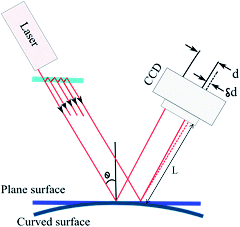 | ||
| Fig. 1 Schematic of in situ curvature measurement during thin film growth by a multiple beam optical stress sensor (MOSS) and determination of stress from the change in curvature by Stoney's equation. | ||
Results and discussion
In our previous report, it was elucidated that deposition rate can be used to control orientations and stresses of YSZ films independently.16 Low deposition rates (<5 nm min−1) during the initial nucleation stages result in (111) oriented films while higher rates (>15 nm min−1) yield (100) oriented films. Also any change in the deposition rate after the initial stage does not change orientation of the film. However, it changes the growth stress. As a result, we are able to independently select texture and stress by nucleating at one rate and carrying out subsequent growth at a different rate.An X-ray diffraction (θ–2θ) scan of a film shows relative density of various grain orientations in the film. As can be noticed in the Fig. 2(a)–(c) that only one peak of YSZ in each plot is present (peaks seen with a star mark belong to the underlying Si) indicating that the YSZ films are textured or oriented. YSZ films deposited at lower rate (0.8 nm min−1) are (111) oriented [Fig. 2(a)], whereas those at higher growth rate (30 nm min−1) are (100) oriented [Fig. 2(b)]. The third pattern [Fig. 2(c)] corresponds to a film that was nucleated and grown at high growth rate (20 nm min−1) for the (100) texture to develop (refer to Narayanachari et al.16 for more details). Following this initial growth, deposition was continued at a slower rate (0.4 nm min−1). As can be noted, the texture does not change and remains as (100). The reason to grow this stack will be apparent later in this paper.
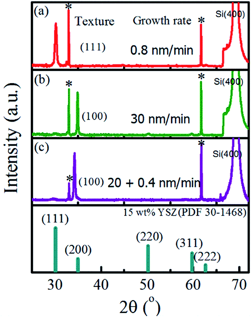 | ||
| Fig. 2 X-ray (θ–2θ) scans showing preferred orientation of YSZ films at different growth rates (a) (111) YSZ at low growth rate (0.8 nm min−1), (b) (100) YSZ at high growth rate (30 nm min−1), (c) (100) YSZ of two layers (initially grown 20 nm min−1 and then 0.4 nm min−1). * indicates peaks from Si substrate, the 33° peak is for the forbidden 200 reflection, whereas the 61° peak is for the 400 reflection due to Cukβ radiation. | ||
As mentioned earlier the aim was to study the effect of film stress on defect densities of YSZ films and hence it is necessary to control stress. In order to have better control over stress, it needs to be monitored during deposition.35 In situ stress measurements of the as-grown (111) and (100) textured YSZ films on Si are as shown in Fig. 3 and 4 respectively. At low rates, films grow in compression, due to adatom injection into grain boundaries, and at higher rates in tension, due to boundary formation, as explained in ref. 16 in great detail. The slope of stress-thickness versus thickness plot is a measure of incremental in-plane stress in a film. Positive slope indicates tensile stress, whereas negative slope indicates compressive stress in a film36 (also see schematic in ESI S-2†). It can be seen in Fig. 3 that with a decrease in the growth rate there is an increase in the magnitude of compressive stress in the (111) oriented films.
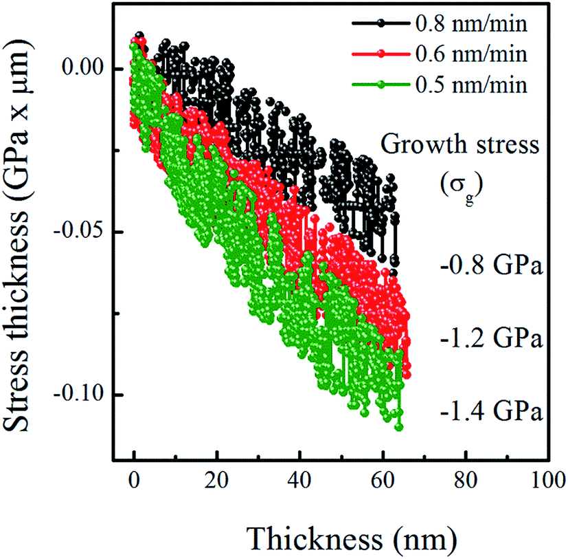 | ||
| Fig. 3 Stress thickness versus thickness plots show the growth stresses for (111) YSZ films deposited at different growth rates. | ||
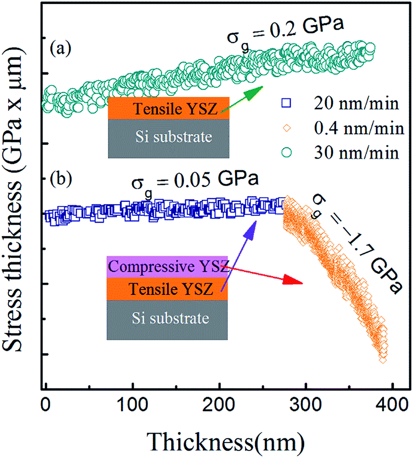 | ||
| Fig. 4 Stress thickness vs. thickness plots show in situ stresses in (100) YSZ films (a) a tensile stressed (grown at 30 nm min−1) and (b) a stack of two layers-a compressive layer (at 0.4 nm min−1) on top of a tensile layer (at 20 nm min−1). Each large division is equivalent to 0.1 GPa μm. | ||
In Fig. 4(a) and (b) the two stress thickness vs. thickness plots of the (100) oriented films correspond to the two XRD patterns shown in Fig. 2(b) and (c) respectively. It can be noticed that a film deposited at high growth rate (30 nm min−1) grows completely under a tensile stress [Fig. 4(a)]. A stack, which was initially deposited at high growth rate (20 nm min−1) for the (100) texture to develop and followed by lower rate (0.4 nm min−1), exhibited a change in growth stress from tensile to compressive [see Fig. 4(b)]. The reason for the deposition of this stack will become clear in the sections to come.
A summary of all the (111) and (100) YSZ films deposited at various deposition rates and having different stresses are presented in the Fig. 5 to give a clear picture in readers' mind.
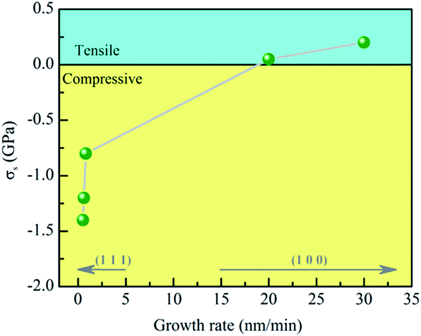 | ||
| Fig. 5 Growth rate dependent steady-state stresses in YSZ films. | ||
The θ–2θ scans indicate that the as-deposited YSZ films are textured in Fig. 2. However, Fig. 6 and 7, ω or rocking curve scans, show that both the as-deposited (111) and (100) films are highly defective as represented by their large FWHM of 16° and 25° respectively.
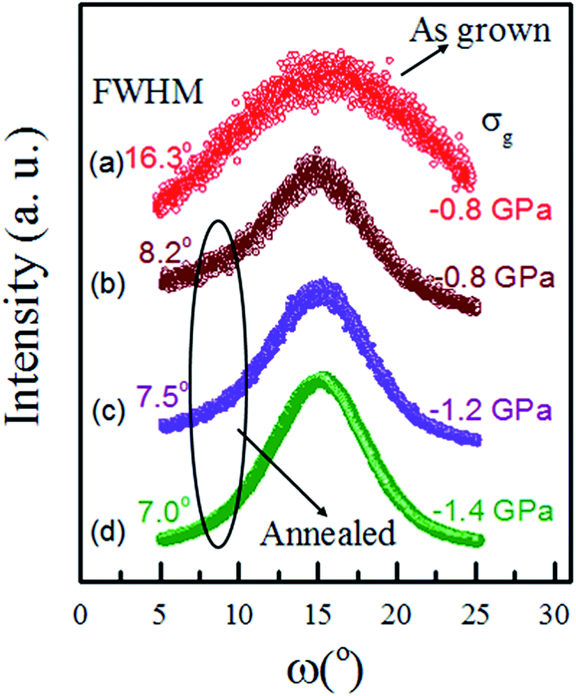 | ||
| Fig. 6 XRD (omega) scans of (111) YSZ films of one as-grown with −0.8 GPa growth stress and some annealed ones with −0.8, −1.2 and −1.4 GPa growth stresses. These plots show reduction in FWHM of rocking curves for higher compressive stressed films after annealing. | ||
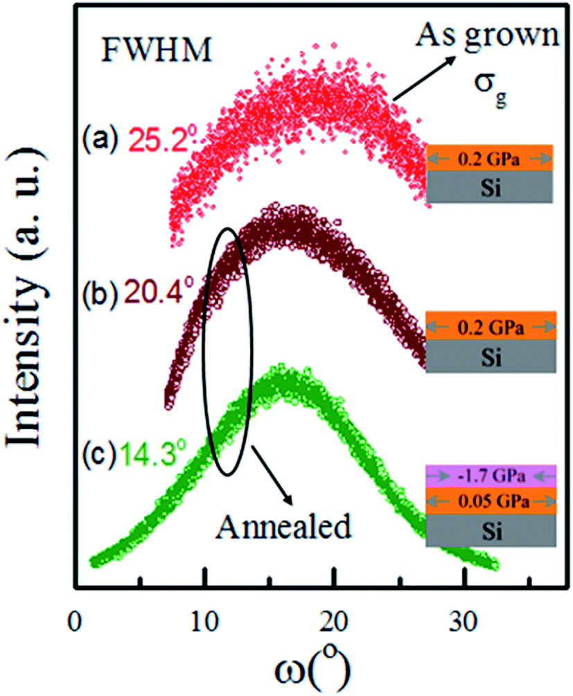 | ||
| Fig. 7 XRD (omega) scans of (100) YSZ films for a tensile stressed (a) as-deposited and (b) annealed film with 0.2 GPa stress, (c) for an annealed film composed of two layers, a compressive layer (−1.7 GPa) on a tensile layer (0.05 GPa). | ||
A summary of the variation in FWHM with growth stress (σg) of the YSZ films is shown in Fig. 8(b). It shows that the FWHM of the rocking curve decrease from 25° to 16° with growth rates ranging from 30 to 0.8 nm min−1 for (100) and (111) YSZ films respectively. This is due to compressive stress driven annealing during growth which will discussed in detail as we go along. Thus, (100) films are more defective than (111) films as (100) YSZ films show larger FWHM than (111) films. A measure of how defective these oxide films are can be gauged from the fact that the as-deposited rocking curve widths of epitaxial III-nitride films on Si are routinely in the 0.1–1° range.
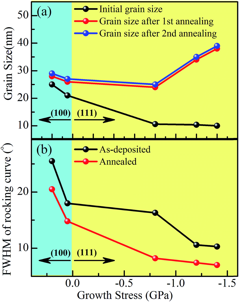 | ||
| Fig. 8 (a) Grain size versus growth stress of as-deposited and annealed films plots show grain-growth on annealing (b) FWHM of rocking curve versus growth stress of as-deposited and annealed films plots show improvement in texture on annealing. | ||
In order to improve crystallinity, the deposited oxide films were annealed at 1000 °C for one hour under ambient condition. The improvement in texture is quite substantial for films with compressive stresses as shown in Fig. 6 and 8. In particular, for the film with a compressive stress of −0.8 GPa, the FWHM was found to reduce by 50% from 16.3 to 8.2. This sharp reduction is accompanied by a 250% increase in the grain size from 20 nm to 70 nm as measured by the AFM scans shown in Fig. 9 (top), also by a 150% increase in vertical coherence length from 10 nm to 25 nm, calculated from X-ray diffraction peak broadening (see ESI S-4, Fig. S3†). In contrast, for tensile stressed (100) YSZ film, the increase in AFM grain size is only 30% [Fig. 9 (bottom)], and 16% as measured from X-ray diffraction peak broadening (see ESI S-4, Fig. S6†). It is hence conclusive that compressive stresses lead to considerable grain-growth of YSZ films. Similar compressive stress-driven grain growth have been observed for metallic films.37,38 Grain growth leads to a reduction in FWHM. The improvement in FWHM of rocking curves implies that larger energy high angle grain boundaries are replaced by lower energy small angle grain boundaries during such growth. Therefore, the reduction in FWHM for the (100) YSZ film is also only 25° to 20°. It can be concluded from these two results that improvement in texture for the compressively stressed film is more compared to the tensile stressed one. It is also observed that improvement in crystallinity during annealing is more with increase in initial compressive stress in these films (see Fig. 6). The lowest FWHM of 7° was achieved in heavily compressively stressed film (see Fig. 6), which is better in terms of crystalline quality than any sputtered (111) YSZ film reported before. In the tensile stressed (100) film FWHM was 20° after annealing. It was observed that compressive stress helped in significant texture improvement for (111) YSZ films. Therefore, to improve the texture of (100) YSZ films further, a compressive layer (∼125 nm) was deposited on top of a (100) tensile layer (∼275 nm) [see schematic in Fig. 4(b)]. The FWHM of this two layered stack after annealing is found to be furthered reduced to 14° [see Fig. 7(c)] which indicates a remarkable improvement in texture. Assuming that the bottom layer has a FWHM of ∼20° as measured for other (100) film [in Fig. 7(b)], at the very least the compressive stress has resulted in a dramatic drop to 14° of the whole stack. The actual FWHM from the top layer alone is expected to be much lower. Thus, even in this case, the compressive top layer has helped significantly to enhance texture of the whole stack.
 | ||
| Fig. 9 (Top two) AFM images (1 × 1 μm2) of a compressively (0.8 GPa) stressed (111) YSZ films on Si (a) as-deposited, (b) annealed respectively. (Bottom two) AFM images (1 × 1 μm2) of a tensile stressed (0.2 GPa) stressed (100) YSZ films on Si (c) as-deposited, (d) annealed respectively. Line profile on the AFM images provided information on grain sizes. | ||
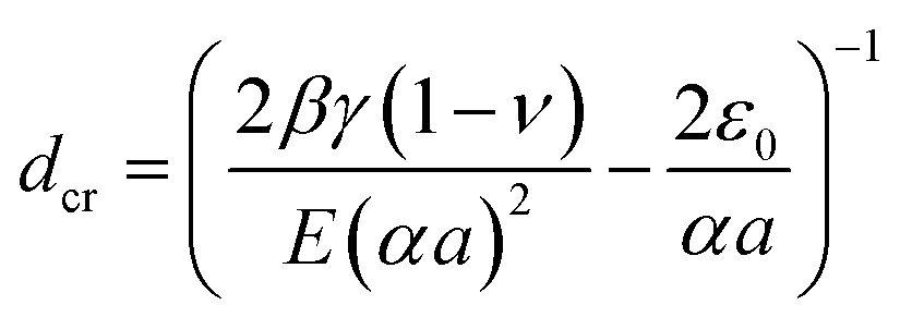
Our observations indicate that compressive stress in as-deposited film helps to improve texture on annealing. This behaviour is now analysed by using Chaudhari's model32 for grain growth upon annealing. In general, the driving force for the grain growth during annealing is the reduction in excess free energy associated with grain boundaries. The densification associated with the reduction in grain boundary area per unit volume however results in shrinkage. For a thin film constrained by a substrate, such shrinkage results into in-plane tensile stress in the film, thereby leading to an increase in the overall mechanical energy of the film. A starting in-plane compressive stress is thus expected to be useful as has already been observed. Grain growth proceeds when the overall change in the energy (ΔEFilm) becomes negative for the process and the ΔEFilm is be expressed as
| ΔEFilm = ΔEStrain + ΔEBoundary |
E, v and γ are Young's modulus, Poison's ratio and grain boundary energy of the film respectively. The values of the above parameters are 220 GPa, 0.3 and 0.5 J m−2 for YSZ respectively.39 ε0 is initial strain in a film and can be determined by initial stress present in the film before annealing divided by modulus. d0 and d are the initial and final grain sizes of the film respectively. a is the lattice parameter and α × a determines the grain boundary width (if α = 1, one unit cell is missing at grain boundaries, here α = 0.87 is used for fitting), β is a geometrical factor (β = 2 for spherical grains). Depending on initial grain size (d0), a plot of change in film energy versus final grain size, could either result in an energy minimum at which the system would stabilize (for d0 < dcr) or not result in one (for d0 > dcr). The dcr (critical grain size) of a film depends on the initial stress in the as-deposited film as described in the below expression and shown in Fig. 10.
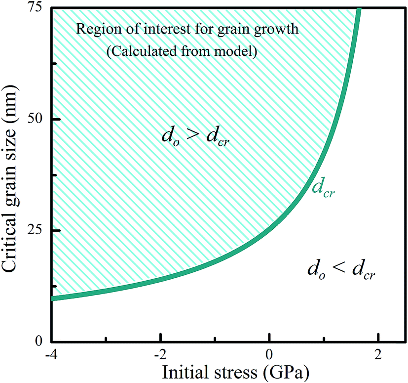 | ||
| Fig. 10 Critical grain size vs. initial stress plot shows dependence of critical grain size on initial in-plane stress in a film. | ||
In the former condition (for d0 < dcr), where there is an energy minimum, grain growth on annealing would be arrested once a system reached the minimum. While in the latter (for d0 > dcr), annealing would result in the continued grain growth and extended generation of a tensile stresses.
In order to apply the model, we use the crystallite size as measured by X-ray line broadening in θ–2θ scans (all the θ–2θ scans of the as-deposited and annealed YSZ films are provided in the ESI S-4†). In doing so, the implicit assumption being made, see ESI S-5,† is that grain size and growth is equiaxed. The starting stress (σo) value used in these calculations is the sum of the growth stress (σg) measured and thermal mismatch stress generated during the heating from growth temperature (700 °C) to the annealing temperature (1000 °C). In the present case the thermal mismatch stress is −0.5 GPa (see ESI S-3†).
Fig. 11 shows the change in film energy vs. final grain size of (111) YSZ films with d0 < dcr. It can be observed that there is an energy minimum for each film. Final grain sizes of these films after annealing matches with the corresponding energy minimum in top of Fig. 11. There is a close match between the experimental values (Fig. 11 top) and the calculated value the model (Fig. 11 bottom). It can also be noticed that higher the initial compressive stress, larger the final grain size.
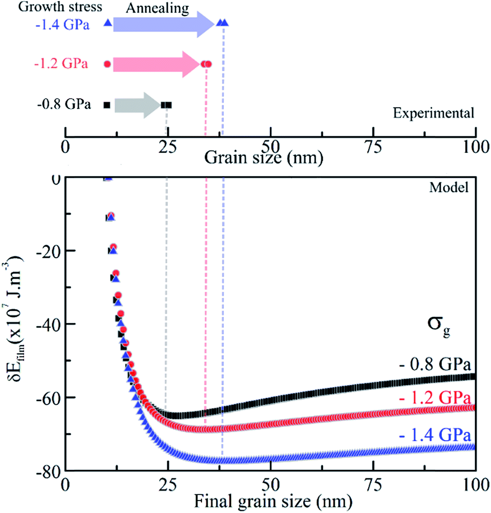 | ||
| Fig. 11 Change in film energy versus final grain size plots, for three (111) YSZ films with d0 < dcr, show energy minima as expected from model. The corresponding top figure shows the final grain sizes after twice annealing and also indicates that grain growth get saturated at their energy minima. | ||
Fig. 12 shows plot of change in film energy vs. final grain size for (100) YSZ films with d0 > dcr. It can be noticed that there is no energy minimum as expected from the energy balance model. However, experimental results in the corresponding top figure shows grain growth saturation at some particular grain size. Note that the x-axis is up to 60 nm to make grain sizes clear, but no energy minimum was found even when x-axis was extended to >150 nm. This contradicts the model which predicts that if d0 > dcr, grain should grow continuously and grain growth should not get saturated.
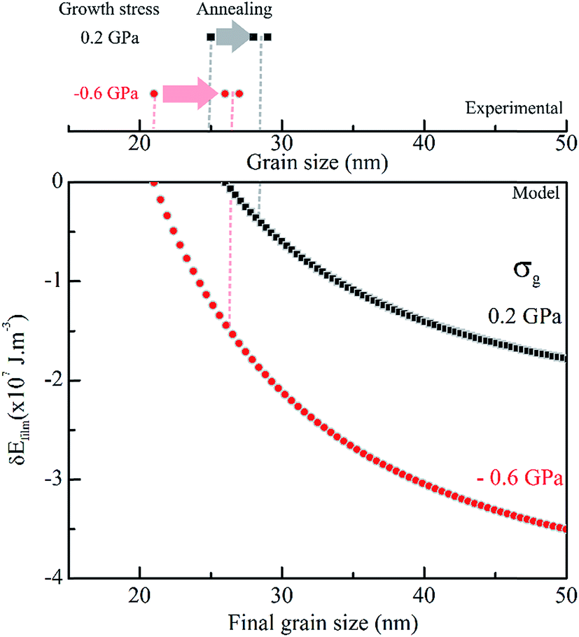 | ||
| Fig. 12 Change in film energy vs. final grain size plots for two (100) YSZ films show no energy minimum as expected from the model. The corresponding top figure shows the final grain sizes after twice annealing and indicates that grain growth saturates at some final grain size. | ||
To confirm whether the grain growth is actually limited by kinetics and not by thermodynamics, two of these films with d0 > dcr were annealed at a higher temperature (1200 °C) for another hour. If there is no grain growth even at this higher temperature, then it can be concluded that the grain growth saturates due to limitation in diffusion of grain boundaries. It was observed that there was hardly any increase in grain size (see Fig. 13). Thus, the obvious reason for the lack of agreement with thermodynamic predictions seems to be due to the kinetics factors. It is to be noticed that the slope of the energy-grain size plot (J m−1 or  ) can be looked upon as a measure of kinetic driving force for grain growth. This slope for a film with d0 < dcr is higher (∼one order of magnitude) than for a film with d0 > dcr (see Fig. 11 and 12). Therefore, kinetic driving force for atomic diffusion aiding grain growth is smaller for the latter case. Hence, grain growth was found to be restricted by kinetics, though thermodynamically there was no restriction for those films with d0 > dcr. While a detailed modelling of grain growth is out of the scope of this paper, it is very well known that the rate of grain growth scales inversely with the grain size.40 This is another reason which supports the experimental observation that there is kinetic limitation for grain growth in (100) YSZ films with d0 > dcr. Thus, while grain growth in a film with large initial grain size (also d0 > dcr) might not be restrained by a thermodynamic minimum, it appears that it will be limited by kinetic factors.
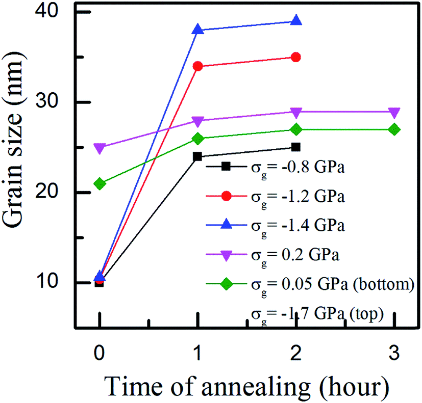 | ||
| Fig. 13 Time of annealing versus grain size plots show grain growths for films with different growth stresses. | ||
Conclusion
In summary, it is shown that annealing of sputtered YSZ/Si films, with tuned growth stress, can lead to remarkable improvement in the orientation of mosaic structures. Deposition of good crystalline quality YSZ films directly on Si is difficult primarily due to the presence of an amorphous native oxide layer at the interface between film and substrate. Here, (100) and (111) textured YSZ films on Si films were deposited by R-DC sputtering. As-deposited films were highly defective and then to improve texture quality, films were annealed. Effect of growth stress on grain-growth and texture-evolution during annealing of these films were studied and analysed by an energy balance model. Grain growth in these films causes generation of in-plane tensile stress during annealing. Hence, it was observed that films with an initial in-plane compressive stress always leads to significant grain growth and hence improvement in texture on annealing. For the first time, the interplay between defects and stress has been utilised for YSZ/Si films and the best quality (111) textured sputtered YSZ/Si(100) films were achieved, though these YSZ films are not close to the state of the art YSZ films by other non-sputtering deposition techniques. This stress driven annealing is an important technique and can be adopted to other films to improve their crystalline quality and corresponding properties.Acknowledgements
The authors acknowledge the support of the Department of Science and Technology (DST), the National Nanofabrication Center (NNFC), and the Micro and Nano Characterization Facility (MNCF) at IISc, Bangalore, funded by MCIT and DST (Grant No. SR/S3/ME/045/2007), Government of India.References
- S. Hall, O. Buiu, I. Z. Mitrovic, Y. Lu and W. M. Davey, Review and perspective of high-k dielectrics on silicon, JTIT, 2007, 2, 33–43 Search PubMed.
- C. H. Ahn, T. Tybell, L. Antognazza, K. Char, R. H. Hammond, M. R. Beasley, Ø. Fischer and J. M. Triscone, Local, Nonvolatile Electronic Writing of Epitaxial Pb(Zr0.52Ti0.48)O3/SrRuO3 Heterostructures, Science, 1997, 276, 1100–1103 CrossRef CAS.
- A. Moezzi, A. M. McDonagh and M. B. Cortie, Zinc oxide particles: synthesis, properties and applications, Chem. Eng. J., 2012, 185, 1–22 CrossRef.
- I. Grekhov, L. Delimova, I. Liniichuk, A. Lyublinsky, I. Veselovsky, A. Titkov, M. Dunaevsky and V. Sakharov, Growth mode study of ultrathin HTSC YBCO films on YBaCuNbO buffer, Phys. C, 1999, 324, 39–46 CrossRef CAS.
- S. Beeby, A. Blackburn and N. White, Processing of PZT piezoelectric thick-films on silicon for microelectromechanical systems, J. Micromech. Microeng., 1999, 9, 218–229 CrossRef CAS.
- K. J. Choi, M. Biegalski, Y. L. Li, A. Sharan, J. Schubert, R. Uecker, P. Reiche, Y. B. Chen, X. Q. Pan, V. Gopalan, L.-Q. Chen, D. G. Schlom and C. B. Eom, Enhancement of Ferroelectricity in Strained BaTiO3 Thin Films, Science, 2004, 306, 1–6 CrossRef PubMed.
- J. Wang, J. B. Neaton, H. Zheng, V. Nagarajan, S. B. Ogale, B. Liu, D. Viehland, V. Vaithyanathan, D. G. Schlom, U. V. Waghmare, N. A. Spaldin, K. M. Rabe, M. Wutting and R. Ramesh, Epitaxial BiFeO3 multiferroic thin film heterostructures, Science, 2003, 299, 1719–1722 CrossRef CAS PubMed.
- J. W. Reiner, A. M. Kolpak, Y. Segal, K. F. Garrity, S. Ismail-Beigi, C. H. Ahn and F. J. Walker, Crystalline Oxides on Silicon, Adv. Mater., 2010, 22, 2919–2938 CrossRef CAS PubMed.
- R. Saleh, S. Wilton, S. Mirabbasi, A. Hu, M. Greenstreet, G. Lemieux, P. P. Pande, C. Grecu and A. Ivanov, System-on-Chip: Reuse and Integration, Proc. IEEE, 2006, 94, 1050–1069 CrossRef.
- T. R. Taylor, P. J. Hansen, B. Acikel, N. Pervez, R. A. York, S. K. Streiffer and J. S. Speck, Impact of thermal strain on the dielectric constant of sputtered barium strontium titanate thin films, Appl. Phys. Lett., 2002, 80, 1978–1980 CrossRef CAS.
- H. C. Li, W. Si, A. D. West and X. X. Xi, Near single crystal-level dielectric loss and nonlinearity in pulsed laser deposited SrTiO3 thin films, Appl. Phys. Lett., 1998, 73, 190–192 CrossRef CAS.
- R. Dittmann, R. Plonka, E. Vasco, N. A. Pertsev, J. Q. He, C. L. Jia, S. H. Eifert and R. Waser, Sharp ferroelectric phase transition in strained single-crystalline SrRuO3/Ba0.7Sr0.3TiO3/SrRuO3 capacitors, Appl. Phys. Lett., 2003, 83, 5011–5013 CrossRef CAS.
- J. Heber, Enter the Oxides, Nature, 2009, 459, 28–30 CrossRef CAS PubMed.
- M. P. Warusawithana, C. Cen, C. R. Sleasman, J. C. Woicik, Y. Li, L. F. Kourkoutis, J. A. Klug, H. Li, P. Rayan, L. P. Wang, M. Bedzyk, D. A. Muller, L. Q. Chen and D. G. Schlom, A ferroelectric oxide made directly on silicon, Science, 2009, 324, 367–370 CrossRef CAS PubMed.
- M. Nagaboopathy, N. Ravishankar and S. Raghavan, Synergistic effect of reactor chemistry and compressive stress on dislocation bending during GaN growth, Appl. Phys. Lett., 2013, 103, 419121–419125 CrossRef.
- K. V. L. V Narayanachari and S. Raghavan, Stress and texture development during sputtering of yttria, zirconia, and yttria stabilized zirconia films on Si substrates, J. Appl. Phys., 2012, 112, 74910–74919 CrossRef.
- K. J. Hubbard and D. G. Schlom, Thermodynamic stability of binary oxides in contact with silicon, J. Mater. Res., 1996, 11, 2757–2776 CrossRef CAS.
- J. Li, P. Wang, J. Y. Xiang, X. H. Zhu, W. Peng, Y. F. Chen, D. N. Zheng and Z. W. Li, Large low-field magnetoresistance observed in twinned La2/3Ca1/3MnO3 thin films epitaxially grown on yttria-stabilized zirconia-buffered silicon on insulator substrates, Appl. Phys. Lett., 2005, 86, 112514–112523 CrossRef.
- R. Aggarwal, C. Jin, P. Pant, J. Narayan and R. J. Narayan, Growth of biepitaxial ZnO thin films on Si(100) using YSZ buffer layer, Appl. Phys. Lett., 2008, 93, 251905 CrossRef.
- X. Zhao and D. Vanderbilt, First-principles study of structural, vibrational, and lattice dielectric properties of hafnium oxide, Phys. Rev. B: Condens. Matter Mater. Phys., 2002, 65, 751051–751110 Search PubMed.
- R. Ramesh and D. G. Schlom, Orienting ferroelectric films, Science, 2002, 296, 1975–1976 CrossRef CAS PubMed.
- D. K. Fork, D. B. Fenner, G. A. N. Connell, J. M. Phillips and T. H. Geballe, Epitaxial yttria-stabilized zirconia on hydrogen-terminated Si by pulsed laser deposition, Appl. Phys. Lett., 1990, 57, 1137–1139 CrossRef CAS.
- P. Legagneux, G. Garry, D. Dieumegard, C. Schwebel, C. Pellet, G. Gautherin and J. Siejka, Epitaxial growth of yttria-stabilized zirconia films on silicon by ultrahigh vacuum ion beam sputter deposition, Appl. Phys. Lett., 1988, 53, 1506–1508 CrossRef CAS.
- S. Horita, T. Tajima, M. Murakawa, T. Fujiyama and T. Hata, Improvement of the crystalline quality of an yttria-stabilized zirconia film on silicon by a new deposition process in reactive sputtering, Thin Solid Films, 1993, 229, 17–23 CrossRef CAS.
- S. Horita, M. Murakawa and T. Fuiyama, Heteroepitaxial Growth of Yttria-Stabilized Zirconia on Silicon (100) by Reactive Sputtering with an Electron Cyclotron Resonance Source, J. Electrochem. Soc., 1999, 146, 1500 CrossRef.
- S. Sønderby, A. J. Nielsen, B. H. Christensen, K. P. Almtoft, J. Lu, J. Jensen, L. P. Nielsen and P. Eklund, Reactive magnetron sputtering of uniform yttria-stabilized zirconia coatings in an industrial setup Zr/Y targets, Surf. Coat. Technol., 2012, 206, 4126–4131 CrossRef.
- M. Migliuolo, a. K. Stamper, D. W. Greve and T. E. Schlesinger, Single target sputtering of superconducting YBa2Cu3O7-δ thin films on Si(100), Appl. Phys. Lett., 1989, 54, 859 CrossRef CAS.
- E. S. Thiele, L. S. Wang, T. O. Mason and S. A. Barnett, Deposition and properties of yttria-stabilized zirconia thin films using reactive direct current magnetron sputtering, J. Vac. Sci. Technol., A, 1991, 9, 3054–3060 CAS.
- Y. Miyahara, Characterization of sputtered yttria-stabilized zirconia thin film and its application to a metal-insulator-semiconductor structure, J. Appl. Phys., 1992, 71, 2309–2314 CrossRef CAS.
- A. K. Stamper, D. W. Greve and T. E. Schlesinger, Deposition of textured yttria-stabilized ZrO2 films on oxidized silicon, J. Appl. Phys., 1991, 70, 2046–2051 CrossRef CAS.
- S. Mahieu, P. Ghekiere, G. De Winter, D. Depla, R. De Gryse, O. I. Lebedev and G. V. Tendeloo, Influence of the Ar/O2 ratio on the growth and biaxial alignment of yttria stabilized zirconia layers during reactive unbalanced magnetron sputtering, Thin Solid Films, 2005, 484, 18–25 CrossRef CAS.
- P. Chaudhari, Grain Growth and Stress Relief in Thin Films, J. Vac. Sci. Technol., 1972, 9, 520–522 CrossRef CAS.
- H. Hidalgo, E. Reguzina, E. Millon, A.-L. Thomann, J. Mathias, C. Boulmer-Leborgne, T. Sauvage and P. Brault, Yttria-stabilized zirconia thin films deposited by pulsed-laser deposition and magnetron sputtering, Surf. Coat. Technol., 2011, 205, 4495–4499 CrossRef CAS.
- S. Gsell, M. Fischer, R. Brescia, M. Schreck, P. Huber and F. Bayer, et al., Reduction of mosaic spread using iridium interlayers: a route to improved oxide heteroepitaxy on silicon, Appl. Phys. Lett., 2007, 91, 1–4 CrossRef.
- S. Suresh and L. B. Freund, Thin Film Materials: Stress, Defect Formation and Surface Evolution, Cambidge, 2003 Search PubMed.
- J. A. Floro, E. Chason, R. C. Cammarata and D. J. Srolovitz, Physical Origins of Intrinsic Stresses in Volmer–Weber Thin Films, MRS Bull., 2002, 27, 19–25 CrossRef CAS.
- Y. Zhang, J. A. Sharon, G. L. Hu, K. T. Ramesh and K. J. Hemker, Stress-driven grain growth in ultrafine grained Mg thin film, Scr. Mater., 2013, 68, 424–427 CrossRef CAS.
- A. M. Engwall, Z. Rao and E. Chason, Origins of residual stress in thin films: Interaction between microstructure and growth kinetics, Mater. Des., 2016, 110, 616–623 CrossRef CAS.
- H. Yoshida, K. Yokoyama, N. Shibata, Y. Ikuhara and T. Sakuma, High-temperature grain boundary sliding behavior and grain boundary energy in cubic zirconia bicrystals, Acta Mater., 2004, 52, 2349–2357 CrossRef CAS.
- H. V. Atkinson, Theories of normal grain growth in pure single phase systems, Acta Metall., 1988, 36, 469–491 CrossRef CAS.
Footnote |
| † Electronic supplementary information (ESI) available. See DOI: 10.1039/c6ra28437j |
| This journal is © The Royal Society of Chemistry 2017 |