
 Open Access Article
 This Open Access Article is licensed under a
 Creative Commons Attribution 3.0 Unported Licence
Dually crosslinkable SiO2@polysiloxane core–shell nanoparticles for flexible gate dielectric insulators†
Eunkyung Leeac,
Jiyoung Junga,
Ajeong Choia,
Xavier Bulliarda,
Jung-Hwa Kimb,
Youngjun Yuna,
Jooyoung Kima,
Jeongil Parka,
Sangyoon Leea and
Youngjong Kang *c
*c
aMaterial Research Center, Samsung Electronics, 130, Samsung-ro, Yeongtong-gu, Suwon-si, Gyeonggi-do 443-803, Korea
bPlatform Technology Lab, Samsung Electronics, 130, Samsung-ro, Yeongtong-gu, Suwon-si, Gyeonggi-do 443-803, Korea
cDepartment of Chemistry, Research Institute for Natural Sciences, Institute of Nano Science and Technology, Hanyang University, 222 Wangsimni-Ro, Seongdong-Gu, Seoul, 04763, Korea. E-mail: youngjkang@hanyang.ac.kr
First published on 23rd March 2017
Abstract
A hybrid gate dielectric material for flexible OTFT is developed by using core–shell nanoparticles (SiO2@PSRXL) where the core and the shell consist of silica nanoparticles and polysiloxane resin, respectively. Since polysiloxane resin contains both thermal- and photo-crosslinkable functional groups, densely-crosslinked thin gate dielectric films can be easily prepared on various substrates by conventional solution casting followed by dual crosslinking. SiO2@PSRXL films exhibit high thermal stability (weight loss at 300 °C is smaller than 3 wt%). The dielectric films made of SiO2@PSRXL show an exceptionally low leakage current and no breakdown voltage up to 4.3 MV cm−1, which are comparable to those of silica dielectrics prepared by CVD. OTFT devices based on dibenzothiopheno[6,5-b:6′,5′-f]thieno[3,2-b]thiophene (DTBTT) as a semiconductor and SiO2@PSRXL as a gate dielectric exhibit good hole mobility (2.5 cm2 V−1 s−1) and Ion/Ioff ratio (106).
1. Introduction
Organic thin film transistors (OTFTs) represent a promising alternative to silicon-based transistors, applicable to low-cost, flexible and large-area electronic devices including radio-frequency identification (RFID) tags, electronic papers, and backplane circuits for active-matrix displays. Remarkable research interest has been directed towards the development of solution-processable organic gate dielectrics as well as organic semiconducting materials.1 Since many electrical properties of OTFTs such as carrier trapping, charge doping, molecular reorientation, dipole formation, and chemical reactions occur at the interface between the semiconductor and gate dielectric,2–6 engineering of gate dielectrics is pivotal for improving the performance of OTFTs. While the SiO2 gate dielectric meets the strict demands for use in inorganic devices, its use in OTFTs is hindered by the need of vacuum deposition techniques. To this end, a few solution-processable polymers including poly(4-vinylphenol) (PVP),7 polyimides (PI),8,9 poly(methyl methacrylate) (PMMA),10 poly(vinyl alcohol) (PVA)11 and others3,12–18 have been demonstrated for organic gate dielectrics. Organosiloxane compounds also have been of interest as a candidate of the solution-processable gate dielectric material because of their structural similarity to SiO2 when they are condensed to polysiloxane.19–23 Various polymer/nanoparticle hybrid gate dielectrics also have been investigated.24–32 Although the performance of organic thin-film transistors (OTFTs) using some of the polymer dielectrics is comparable to those using SiO2 dielectrics in terms of charge mobility,7,14,15,33 many problems including large hysteresis of threshold voltage, high leakage current, and high operating voltage are not fully addressed yet.11,34,35In this study, we report a solution processable gate insulating material based on dually crosslinkable core–shell nanoparticles (SiO2@PSRXL). The SiO2@PSRXL nanoparticles consist of silica nanoparticle core and polysiloxane shell which contains thermal- and photo-crosslinkable functional groups. Because polysiloxane shells are chemically bounded on the surface of SiO2 nanoparticles, SiO2@PSRXL nanoparticles can be well dispersed in common organic solvents and form transparent and uniform gate insulating films without nanoparticle aggregation. The core–shell geometry makes minimize the formation of interstitial voids and enhance the performance of the dielectric films comparable to the conventional SiO2 dielectric layers formed by vacuum deposition. SiO2@PSRXL gate dielectric films were prepared by two-step reaction. As shown in Fig. 1, the chemical linkages between the surface of SiO2 and polysiloxane were first created by hydrolysis/condensation, and then subsequently the residual epoxy and acrylate groups on the polysiloxane chains were crosslinked at the second stage. This two-step reaction leads the uniform and highly dense SiO2@PSRXL gate dielectric films. In this sense, our work is different from other examples based on the polymer/nanoparticles composites.24–32
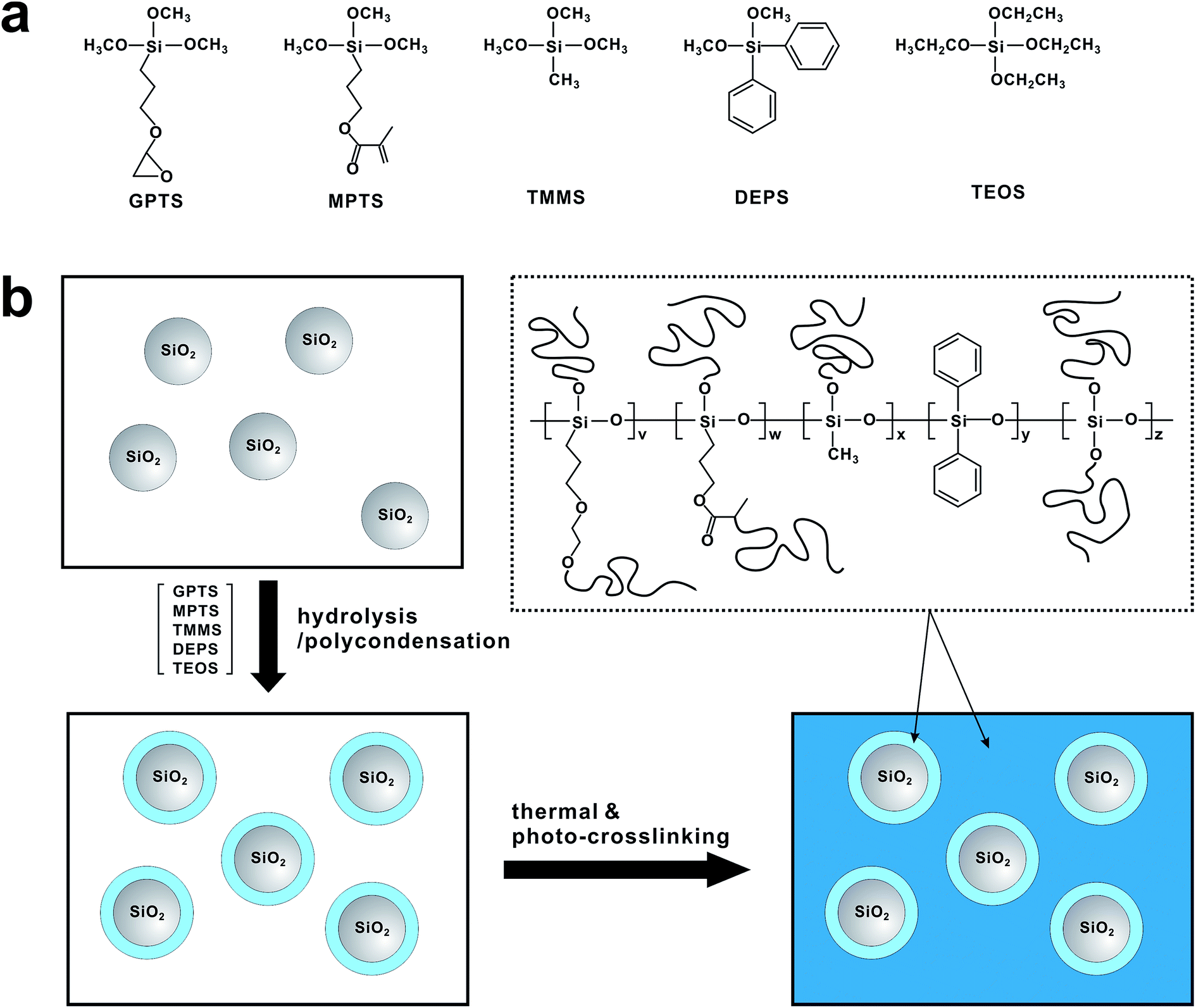 | ||
| Fig. 1 (a) Chemical structure of siloxane monomers. (b) Synthetic scheme of SiO2@PSRXL. | ||
2. Result and discussion
Homogeneous dispersion of silica nanoparticles in polysiloxane resin is pivotal for high performance of the gate dielectric films. To incorporate silica nanoparticles into the polysiloxane matrix, we have utilized the hydrolysis/condensation reaction between the hydroxyl groups on the surface of nanoparticle and siloxane monomers. Briefly, silica nanoparticles (daverage = 10 ± 5 nm) was first treated with strong acid to make abundant hydroxyl groups on the silica surface. Those hydroxyl groups were then used to react with the monomer mixture including (3-glycidyloxypropyl)trimethoxysilane (GPTS), [3-(methacryloyloxy)propyl]trimethoxysilane (MPTS), trimethoxymethylsilane (TMMS), diethoxydiphenylsilane (DEPS) and tetraethoxysilane (TEOS). In this case, GPTS and MPTS were introduced to conduct thermal- and photo-curing at the second stage. Furthermore, the propyl side chains increase the flexibility. TMMS and DEPS were added to increase the mechanical flexibility and electrical properties of the gate dielectric films, respectively.36–38 Finally TEOS was introduced to compensate the deficient reaction sites occupied by the phenyl groups of DEPS.39 The composition of the monomer mixture was optimized to 15 mol%, 20 mol%, 35 mol%, 15 mol% and 15 mol% for GPTS, MPTS, TMMS, DEPS and TEOS respectively. The SiO2 nanoparticle content was controlled to 20 wt% of the whole monomer mixture. Under the acidic condition, polysiloxane networks formed around the silica nanoparticles. In this case, the hydrolysis/condensation reaction condition was carefully controlled not to form gels by overshoot reaction. Viscosity of the resulting SiO2@PSR core–shell nanoparticle solution was 9.2 cps at 20 °C, and well dispersed in polar solvents such as propylene glycol monomethyl ether acetate (PGMEA). To check the extent of polymerization, a pure polysiloxane resin without nanosilica (PSR) was synthesized at the same condition, and the molecular weight was measured on a GPC (Mw = 2200 g mol−1, PDI = 1.39).The structure of SiO2@PSR was characterized by SEM and SAXS. As shown in Fig. 2a, SEM micrograph of the dried SiO2@PSR shows many isolated particulates with an average diameter of 28 ± 2.5 nm which is significantly larger than that of the original silica nanoparticles (daverage = 10 ± 5 nm). Furthermore, nanoparticles show the core–shell structure with ∼10 nm size of core. These results imply that polysiloxane networks dominantly form around SiO2 nanoparticles by surface initiated polycondensation reaction. Unlike SiO2@PSR, pure PSR sample does not show particulates (Fig. 2b). To understand the structure of SiO2@PSR nanoparticles in solution, SAXS analysis has been done in the liquid phase. Fig. 2c and d show SAXS data of SiO2@PSR and PSR respectively. The shape and size of two samples were obtained from their scattering profiles. Pair-distance distribution function for each sample was obtained by using the indirect Fourier transform.28 The calculated scattering curves from the distribution functions (red solid lines) show good agreement with the experimental data (black dots). SAXS analysis confirms that SiO2@PSR nanoparticles are circular particles with a diameter of 28 nm which is consistent with the previous SEM analysis. SAXS analysis also shows that the size of PSR is 2 nm.
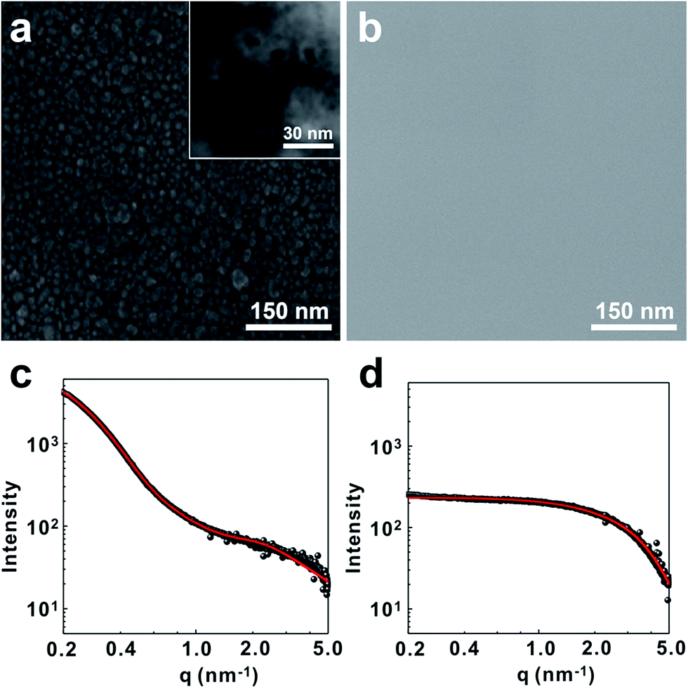 | ||
| Fig. 2 SEM micrographs of (a) SiO2@PSR and (b) PSR. SAXS data of (c) SiO2@PSR and (d) PSR. | ||
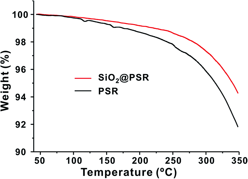
Thermal properties of SiO2@PSR and PSR were characterized on a TGA. As shown in Fig. 3, SiO2@PSR showed the better thermal stability than PSR. The weight loss of SiO2@PSR (5.7 wt%) was smaller than that of PSR (8.8 wt%) at 350 °C. As increasing the temperature, the both weight curves of SiO2@PSR and PSR gradually decreased from the relatively low temperature (∼150 °C), which indicates the presence of the unreacted residual monomers. Utilizing those many remnant reactive groups, we made dense dielectric films by using thermal- and photo-crosslinking reaction at the second-stage.
 | ||
| Fig. 3 TGA graphs of SiO2@PSR and PSR. | ||
Since the SiO2@PSR can be well dispersed in polar organic solvents, uniform dielectric films can be easily prepared by spin casting. For preparing metal–insulator–metal (MIM) devices, dielectric films were first prepared on the molybdenum-coated glass slides by spin coating from a 35 wt% of SiO2@PSR solution in PGMEA. The film thickness was controlled to 500 ± 50 nm. The films were then crosslinked by thermal and photo annealing (the crosslinked SiO2@PSR film will be notated as SiO2@PSRXL). Briefly, the SiO2@PSR films were first soft-baked at 70 °C for 15 min to activate the epoxy/hydroxyl groups, and simultaneously exposed to UV (λband = 240–400 nm) for 75 s to induce photo-crosslinking. To complete the crosslinking reaction, the films were annealed at 200 °C for 1 h under the nitrogen atmosphere. FT-IR analysis confirms that MPTS units polymerize during the photo-crosslinking process (Fig. S1†). The characteristic ethylene peaks of MPTS at 1637 cm−1 and 810 cm−1 disappeared, and the carbonyl peak was shifted from 1727 cm−1 to 1733 cm−1 after photo-crosslinking process. The disappearance of ethylene peak and the shift of carbonyl peak in FT-IR was attributed to the polymerization of acrylate groups of MPTS. After the crosslinking process, gold was evaporated on the films to make the top electrode. For comparison, MIM devices using pure PSR were also prepared following the same procedure.
The leakage current density of the MIM devices was measured as a function of electric field (Fig. 4). The MIM devices based on SiO2@PSRXL showed very low leakage current, ∼10−8 A cm−2 at 2 MV cm−1 of the applied voltage, which is 2 orders lower than that of the MIM based on PSRXL. No breakdown behavior was observed at least up to 4.3 MV cm−1, which is significantly higher than that of other polymer or polysiloxane gate insulators typically showing breakdown in the range of 1.5–2.5 MV cm−1.40 In terms of the breakdown strength, our dielectric films based on SiO2@PSRXL are comparable to the silica films prepared by CVD method.41,42 We attribute such high breakdown strength and low leakage current to the dense network structure made of core–shell-type SiO2@PSRXL nanoparticles. The dielectric constant of SiO2@PSRXL (ε = 4.26 at 1 kHz) measured on the MIM device was comparable to that of PSRXL (ε = 4.30 at 1 kHz) (Fig. S2†).
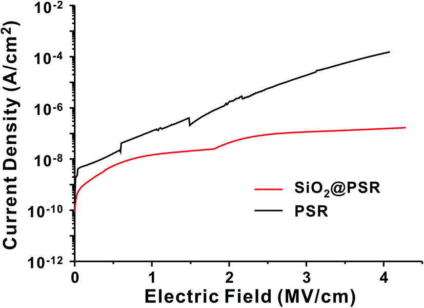 | ||
| Fig. 4 The changes of leakage current density as a function of electric field for SiO2@PSR and PSR films. | ||
SiO2@PSRXL gate dielectric films were tested for the organic thin film transistor (OTFT). In our experiments, a thiophene-rich heteroacene derivative, dibenzothiopheno[6,5-b:6′,5′-f]thieno[3,2-b]thiophene (DTBTT)43 was used as an active material (Fig. 5a). DTBTT was synthesized following the previously reported procedures.43 For the fabrication of OFET transistors, SiO2@PSRXL films were first prepared on the glass substrates patterned with molybdenum gate electrodes with a thickness of 550 nm following the previously described procedures.44 DTBTT was then vacuum-deposited on the SiO2@PSRXL films. Finally, the gold source and drain electrodes were formed on the DTBTT by using the conventional vacuum deposition technique. The channel width and length of the devices were 1000 and 100 μm, respectively. Fig. 5b represents a SEM micrograph of the cross-section of the device prepared by using focused ion beam (FIB) technique. It is notable that the gate insulator layer is very uniform and flat with considering that it was prepared by the wet coating process. For comparison, OFET devices based on PSRXL were also prepared following the same procedures. As shown in Fig. 5c and d, the devices based on SiO2@PSRXL showed much better performance than that of PSRXL. The hole mobility and the Ion/Ioff ratio was 2.5 ± 0.13 cm2 V−1 s−1 and 106 respectively for the OFET device based on SiO2@PSRXL, while they were 0.9 ± 0.07 cm2 V−1 s−1 and 104 for the device based on PSRXL. Furthermore, it was noticed that the off-current of the device based on SiO2@PSRXL was lowered than the PSRXL sample.
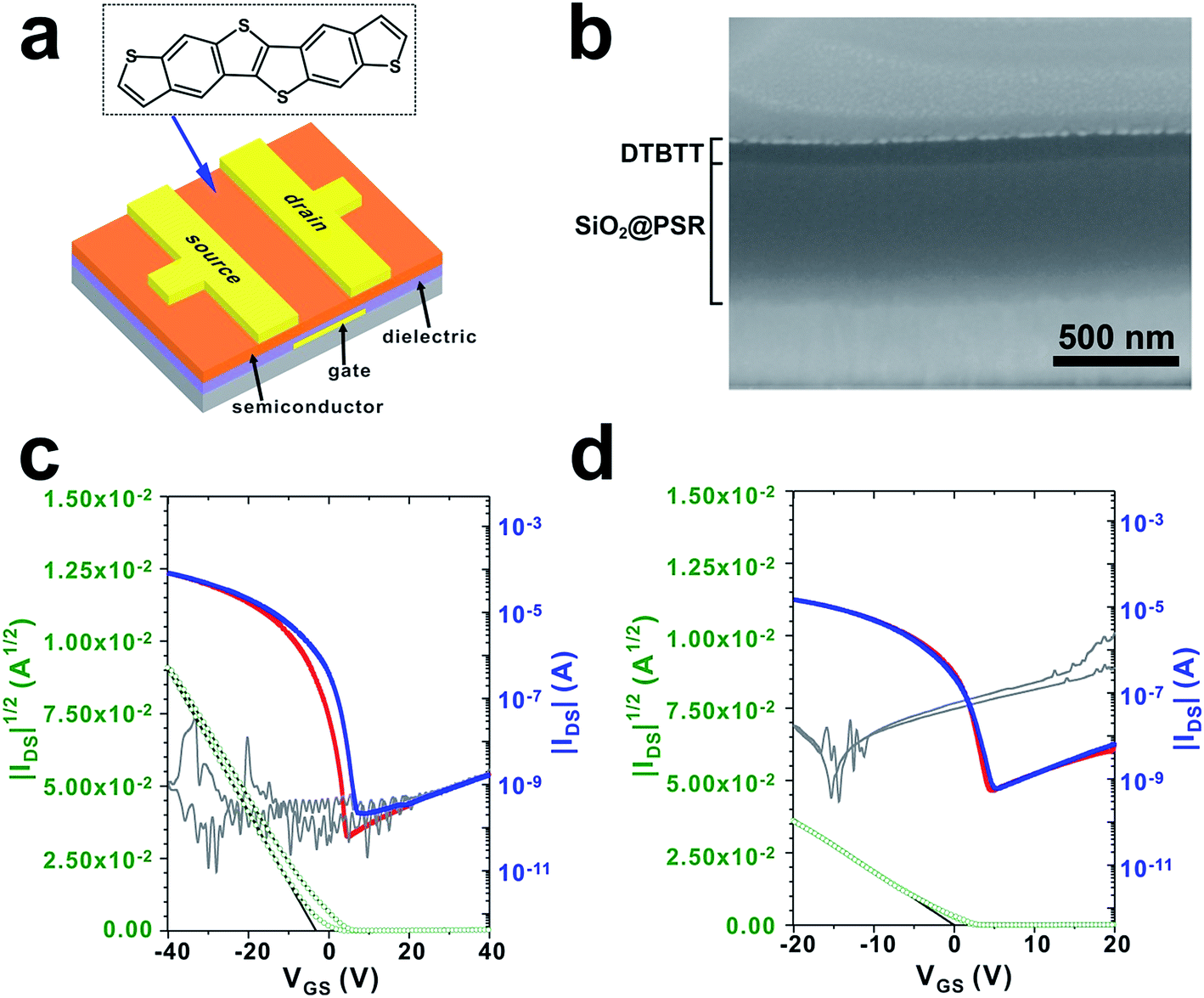 | ||
| Fig. 5 (a) The chemical structure of DTBTT and the schematic structure of DTBTT OFET. (b) SEM micrograph of a cross-section of the fabricated OFET. The representative transfer characteristics of DTBTT OFET fabricated on (c) SiO2@PSRXL and (d) PSRXL gate dielectric. The average hole mobility obtained from 16 devices was μFET = 2.5 ± 0.13 cm2 V−1 s−1 for SiO2@PSRXL and μFET = 0.9 ± 0.07 cm2 V−1 s−1 for PSRXL, respectively. | ||
The fabrication process of SiO2@PSRXL films is applicable for the plastic substrates (Fig. 6a). Similar to the above-mentioned procedures, SiO2@PSR solution was spun on the Al patterned polyimide substrate, and cured by heating and UV treatment. In this case, the annealing temperature was lowered to 60 °C while it was 200 °C for the fabrication on glass substrates. The thickness was same as 550 nm. AFM image showed that the RMS roughness increased slightly from 4.5 Å to 6 Å comparing with the sample prepared on glass (Fig. 6b). DTBTT was then deposited by thermal evaporation, and finally gold source/drain electrodes were evaporated thereto. The hole mobility and the Ion/Ioff ratio for the sample was 0.88 ± 0.04 cm2 V−1 s−1 and 105 respectively (Fig. 6c and d).
 | ||
| Fig. 6 (a) Photograph of DTBTT OFET devices fabricated on a PI substrate. (b) AFM micrograph of SiO2@PSRXL film coated on PI substrate. (c) Transfer and (d) output characteristics of DTBTT OFET devices fabricated on a PI substrate. The average hole mobility obtained from 16 devices was μFET = 0.88 ± 0.04 cm2 V−1 s−1. | ||
3. Conclusion
In summary, we have successfully demonstrated a novel gate dielectric material for OTFT by incorporating SiO2 nanoparticles into polysiloxane matrix. The two-step process, formation of colloidal core–shell nanoparticles and subsequent double-crosslinking, leads to form uniform and dense organic/inorganic composite dielectric films by using the conventional solution process. SiO2@PSRXL films showed not only good thermal and mechanical properties but also outstanding electrical properties. The dielectric films made of SiO2@PSRXL showed exceptionally low leakage current and no breakdown voltage up to 4.3 MV cm−1, which are comparable to those of silica dielectrics prepared by CVD. Their excellent dielectric properties were also reflected in the performance of OTFT. The OFET device based on SiO2@PSRXL exhibited the much better mobility and Ion/Ioff ratio than its counterpart made of PSRXL. Our approach is versatile since it can be easily expended to other nanoparticles including TiO2 and ZnO, and the physical properties can be easily tuned by monomer compositions.4. Experimental
(1) Synthesis of SiO2@PSR
Aqueous alkaline silica sol (500 g) was passed through a column charged with acidic cationic exchange resin, obtaining acidic silica sol having pH = 2. The collected acidic silica sol (500 g) and methanol (1000 mL) were then charged in a reactor equipped with a reflux condenser and a mechanical stirrer. Subsequently, (3-glycidyloxypropyl)trimethoxysilane (GPTS, 11 g, 0.05 mol) was added to the reactor. The mixture was well mixed for 1 h, and then the temperature increased to 95 °C, and sit for 6 h. To remove water from the silica sol, vacuum distillation was performed. After removing water, methanol (1000 mL) was recharged to disperse the silica sol. Trimethoxymethylsilane (TMMS, 43 g, 0.32 mol), (3-glycidyloxypropyl)trimethoxysilane (GPTS, 89 g, 0.38 mol), 3-(methacryloxypropyl)trimethoxysilane (MPTS, 183 g, 0.73 mol), diethoxydiphenylsilane (DEPS, 86 g, 0.32 mol) and tetraethoxysilane (TEOS, 66 g, 0.32 mol) were added to the silica sol, and the mixture was mixed well at room temperature for 1 h. Following this, hydrochloric acid aqueous solution (56 g, 0.1 N) was added in dropwise for 2 h, and the mixture was additionally stirred at room temperature for 2 h to perform hydrolysis reaction. The reaction temperature was then increased to 80 °C and sit for 36 h to induce polycondensation reaction. The resulting SiO2@PSR showed the core–shell structure having SiO2 core and polysiloxane shell. Viscosity of SiO2@PSR was 9.2 cPs at 20 °C, and pH was 5. SiO2@PSR was redispersible in polar organic solvents. In our experiments, SiO2@PSR was dispersed in propylene glycol monomethyl ether acetate (PGMEA) with a concentration of 35 wt%.(2) Synthesis of PSR
TMMS (43 g, 0.32 mol), GPTS (89 g, 0.38 mol), MPTS (183 g, 0.73 mol), DEPS (86 g, 0.32 mol) and TEOS (66 g, 0.32 mol) were charged in a flask and stirred at room temperature. Hydrochloric acid aqueous solution (56 g, 1 N) was then added thereto in dropwise for 2 h, and the mixture was stirred at room temperature for 2 h. The mixture was heated to 80 °C and maintained for 36 h to perform polycondensation. The resulting PSR showed a viscosity of 8.6 cP at 20 °C, pH = 5, and the molecular weight measured on a GPC of 2200 g mol−1 (PDI = 1.39). PSR was dispersed in PGMEA with a concentration of 35 wt%.(3) Fabrication of MIM devices
SiO2@PSR was first spin-casted on molybdenum-coated glass substrates from 35 wt% of solutions in PGMEA. The thickness was controlled to 500 ± 10 nm. SiO2@PSR films were first soft-baked at 70 °C for 15 min to activate the epoxy/hydroxyl groups, and simultaneously exposed to UV (λband = 240–400 nm) for 75 s to induce photo-crosslinking. To complete the crosslinking reaction, the films were annealed at 200 °C for 1 h under the nitrogen atmosphere. After the crosslinking process, gold was evaporated on the SiO2@PSRXL films to make the top electrode.(4) Fabrication of OTFT devices
Molybdenum was sputtered on glass substrates to make gate electrodes. SiO2@PSR was spin-coated thereto from 35 wt% of solutions in PGMEA. The films were first soft-baked at 70 °C for 15 min to activate the epoxy/hydroxyl groups, and simultaneously exposed to UV for 75 s to induce photo-crosslinking. The films were then annealed at 200 °C for 1 h under the nitrogen atmosphere for crosslinking. Dibenzothiopheno[6,5-b:6′,5′-f]thieno[3,2-b]thiophene (DTBTT) was vacuum-deposited on to the films. Finally, gold was sputtered on the DTBTT layer to make source/drain electrodes.Acknowledgements
This work was supported by the Global Leading Technology Program funded by the Ministry of Trade, Industry and Energy, Republic of Korea (10042419), and Basic Science Research Program through the National Research Foundation of Korea (NRF) funded by the Ministry of Education (2012R1A6A1029029).References
- R. P. Ortiz, A. Facchetti and T. J. Marks, Chem. Rev., 2009, 110, 205–239 CrossRef PubMed.
- C. Kim, A. Facchetti and T. J. Marks, Science, 2007, 318, 76–80 CrossRef CAS PubMed.
- P. O. Jackson, M. O'Neill, W. L. Duffy, P. Hindmarsh, S. M. Kelly and G. J. Owen, Chem. Mater., 2001, 13, 694–703 CrossRef CAS.
- C. Kim, Z. Wang, H.-J. Choi, Y.-G. Ha, A. Facchetti and T. J. Marks, J. Am. Chem. Soc., 2008, 130, 6867–6878 CrossRef CAS PubMed.
- L. Kaake, Y. Zou, M. Panzer, C. Frisbie and X.-Y. Zhu, J. Am. Chem. Soc., 2007, 129, 7824–7830 CrossRef CAS PubMed.
- S. Y. Yang, K. Shin and C. E. Park, Adv. Funct. Mater., 2005, 15, 1806–1814 CrossRef CAS.
- H. Klauk, M. Halik, U. Zschieschang, G. Schmid, W. Radlik and W. Weber, J. Appl. Phys., 2002, 92, 5259–5263 CrossRef CAS.
- T. Ahn, J. W. Kim, Y. Choi and M. H. Yi, Org. Electron., 2008, 9, 711–720 CrossRef CAS.
- S. Pyo, M. Lee, J. Jeon, J. H. Lee, M. H. Yi and J. S. Kim, Adv. Funct. Mater., 2005, 15, 619–626 CrossRef CAS.
- J. Puigdollers, C. Voz, A. Orpella, R. Quidant, I. Martın, M. Vetter and R. Alcubilla, Org. Electron., 2004, 5, 67–71 CrossRef CAS.
- T. B. Singh, N. Marjanovic, P. Stadler, M. Auinger, G. Matt, S. Gunes, N. Sariciftci, R. Schwodiauer and S. Bauer, J. Appl. Phys., 2005, 97, 083714 CrossRef.
- L.-L. Chua, P. K. Ho, H. Sirringhaus and R. H. Friend, Appl. Phys. Lett., 2004, 84, 3400–3402 CrossRef CAS.
- J. Ghim, K.-J. Baeg, Y.-Y. Noh, S.-J. Kang, J. Jo, D.-Y. Kim, S. Cho, J. Yuen, K. Lee and A. J. Heeger, Appl. Phys. Lett., 2006, 89, 202516 CrossRef.
- J. Jang, S. Nam, J. Hwang, J.-J. Park, J. Im, C. E. Park and J. M. Kim, J. Mater. Chem., 2012, 22, 1054–1060 RSC.
- H. S. Lee, K. Park, J.-D. Kim, T. Han, K. H. Ryu, H. S. Lim, D. R. Lee, Y.-J. Kwark and J. H. Cho, J. Mater. Chem., 2011, 21, 6968–6974 RSC.
- J. Li, Z. Sun and F. Yan, Adv. Mater., 2012, 24, 88–93 CrossRef CAS PubMed.
- C. H. Wang, C. Y. Hsieh and J. C. Hwang, Adv. Mater., 2011, 23, 1630–1634 CrossRef CAS PubMed.
- D. Gaspar, S. Fernandes, A. De Oliveira, J. Fernandes, P. Grey, R. Pontes, L. Pereira, R. Martins, M. Godinho and E. Fortunato, Nanotechnology, 2014, 25, 094008 CrossRef CAS PubMed.
- K. Kim, E. Lee, S. Y. Park, K.-H. Lim, C. Shin and Y. S. Kim, J. Mater. Chem. C, 2013, 1, 7742–7747 RSC.
- Y.-g. Ha, S. Jeong, J. Wu, M.-G. Kim, V. P. Dravid, A. Facchetti and T. J. Marks, J. Am. Chem. Soc., 2010, 132, 17426–17434 CrossRef CAS PubMed.
- A. Tewari, S. Gandla, A. R. Pininti, K. Karuppasamy, S. Böhm, A. R. Bhattacharyya, C. R. McNeill and D. Gupta, Appl. Phys. Lett., 2015, 107, 103302 CrossRef.
- Z. Ren and S. Yan, Prog. Mater. Sci., 2016, 83, 383–416 CrossRef CAS.
- A. Dadvand, J. Lu, C. Py, T.-Y. Chu, R. Movileanu and Y. Tao, Org. Electron., 2016, 30, 213–218 CrossRef CAS.
- A. Maliakal, H. Katz, P. M. Cotts, S. Subramoney and P. Mirau, J. Am. Chem. Soc., 2005, 127, 14655–14662 CrossRef CAS PubMed.
- R. Schroeder, L. A. Majewski and M. Grell, Adv. Mater., 2005, 17, 1535–1539 CrossRef CAS.
- H. Noh, Y. Seol, S. Kim and N.-E. Lee, Electrochem. Solid-State Lett., 2008, 11, H218–H221 CrossRef CAS.
- B.-U. Hwang, D.-I. Kim, S.-W. Cho, M.-G. Yun, H. J. Kim, Y. J. Kim, H.-K. Cho and N.-E. Lee, Org. Electron., 2014, 15, 1458–1464 CrossRef CAS.
- Y.-G. Ha, K. Everaerts, M. C. Hersam and T. J. Marks, Acc. Chem. Res., 2014, 47, 1019–1028 CrossRef CAS PubMed.
- J. S. Kwon, H.-W. Park, D. H. Kim and Y.-J. Kwark, ACS Appl. Mater. Interfaces, 2017, 9, 5366–5374 CAS.
- Y. M. Park, A. Desai, A. Salleo and L. Jimison, Chem. Mater., 2013, 25, 2571–2579 CrossRef CAS.
- K. Kim, H. W. Song, K. Shin, S. H. Kim and C. E. Park, J. Phys. Chem. C, 2016, 120, 5790–5796 CAS.
- X. Huang and P. Jiang, Adv. Mater., 2015, 27, 546–554 CrossRef CAS PubMed.
- S. Nelson, Y.-Y. Lin, D. Gundlach and T. Jackson, Appl. Phys. Lett., 1998, 72, 1854–1856 CrossRef CAS.
- G. Gu, M. G. Kane, J. E. Doty and A. H. Firester, Appl. Phys. Lett., 2005, 87, 243512 CrossRef.
- H. E. Katz, X. M. Hong, A. Dodabalapur and R. Sarpeshkar, J. Appl. Phys., 2002, 91, 1572–1576 CrossRef CAS.
- P. Liu, Y. Wu, Y. Li, B. S. Ong and S. Zhu, J. Am. Chem. Soc., 2006, 128, 4554–4555 CrossRef CAS PubMed.
- Z. Li, D.-s. Tan, Q.-l. Ren, Y.-f. Xu and Y.-f. Tao, Chin. J. Polym. Sci., 2013, 31, 363–370 CrossRef CAS.
- T. M. Gädda and W. P. Weber, J. Polym. Sci., Part A: Polym. Chem., 2006, 44, 3629–3639 CrossRef.
- M. Alexandru, M. Cazacu, F. Doroftei, M. Ignat, D. Timpu, C. Grigoras and B. Simionescu, eXPRESS Polym. Lett., 2011, 5, 188–196 CrossRef CAS.
- S. Y. Yang, S. H. Kim, K. Shin, H. Jeon and C. E. Park, Appl. Phys. Lett., 2006, 88, 173507 CrossRef.
- P. Solomon, J. Vac. Sci. Technol., 1977, 14, 1122–1130 CrossRef CAS.
- M. Nafria, J. Sune and X. Aymerich, Microelectron. Reliab., 1996, 36, 871–905 CrossRef.
- J.-I. Park, J. W. Chung, J.-Y. Kim, J. Lee, J. Y. Jung, B. Koo, B.-L. Lee, S. W. Lee, Y. W. Jin and S. Y. Lee, J. Am. Chem. Soc., 2015, 137, 12175–12178 CrossRef CAS PubMed.
- C. Reese, M. Roberts, M.-m. Ling and Z. Bao, Mater. Today, 2004, 7, 20–27 CrossRef CAS.
Footnote |
| † Electronic supplementary information (ESI) available. See DOI: 10.1039/c6ra28230j |
| This journal is © The Royal Society of Chemistry 2017 |