
 Open Access Article
 This Open Access Article is licensed under a
 Creative Commons Attribution 3.0 Unported Licence
Fabrication and behaviors of CdS on Bi2MoO6 thin film photoanodes
Hao Yanga,
Zhiliang Jin *a,
Hongyan Hu*b,
Gongxuan Lub and
Yingpu Bib
*a,
Hongyan Hu*b,
Gongxuan Lub and
Yingpu Bib
aSchool of Chemistry and Chemical Engineering, Beifang University of Nationalities, Yinchuan 750021, P. R. China
bState Key Laboratory for Oxo Synthesis and Selective Oxidation, Lanzhou Institute of Chemical Physics, Chinese Academy of Science, Lanzhou 730000, P. R. China
First published on 9th February 2017
Abstract
Most Bi-based photoelectrodes have suitable band gaps and can effectively promote hydrogen evolution from water splitting, but there are few studies up to now for simple preparation methods for Bi-based binary metal oxides as photoanodes. Here, we prepared a novel Bi2MoO6 thin film photo-anode without a template; our preparation methods of Bi-based binary metal oxides with controlled morphologies were conducted by growing the Bi2MoO6 directly on an electrical substrate via an in situ growth process. The photoanodes show well-shaped thin film morphologies and exhibit impressive photoelectrochemical properties compared to the Bi-based photoanodes synthesized by conventional methods. A 2× enhanced photocurrent was obtained when the Bi2MoO6 thin film photoanodes were modified with CdS in comparison with the primary Bi2MoO6 (about 0.85 mA cm−2) under identical conditions. The enhanced photoelectrochemical properties were studied using several techniques including SEM, XRD, XPS, UV-vis diffuse reflectance, etc. and the results were in good agreement with each other. Moreover, the Bi2MoO6 thin film photoanodes possess long-term stability under solar irradiation and show a considerable photocurrent.
1. Introduction
Photoelectrochemical (PEC) water splitting, as a promising strategy for a renewable energy supplement and environmental protection, has attracted worldwide attention.1–3 The determining factor for efficient water splitting is development of a semiconductor photoanode which has rapid charge transfer, a wide absorption spectrum, and excellent stability.4,5,6 However, the traditional way of synthesizing photoanodes limits widespread application due to small specific surface area, low visible light responses, and serious charge recombination problems.7–10 Therefore, developing a new material with high efficiency, durability, easy preparation, and low cost of manufacturing is extremely urgent. Cheng et al. developed various methods of preparing TiO2 photoelectrodes and obtained excellent results.11,12 Recently, Yu et al. synthesized a new type of TiO2 photoelectrode which directly grows on fluorine-doped tin oxide (FTO) using TiCl3 mediated surface treatment of TiO2 nanorods that were designed and fabricated.10,13 Furthermore, TiO2 thin film electrodes were successfully synthesized by Zhang et al.14 using a sol–gel method and the maximum photocurrent value was only 0.5 mA cm−2. We prepared well-aligned ZnO nanowire arrays, by adding other semiconductors, such as BiMoO6 and Au, which significantly enhanced the photoelectrochemical properties.15,16 Attaching substrates increased surface area that was conducive to improved photocurrent due to better transportation of charge carriers and more reactive sites.Compared with single metal oxides, very few simple and effective preparation methods of binary metal oxides have been developed. Binary metal oxides containing Bi(III) have been identified as promising semiconductor electrodes in solar energy conversion. For example, perovskite bismuth ferrite (BiFeO3) with a direct band-gap of approximately 2.2 eV is a promising multifunctional material that also exhibits photocatalytic properties.17,18 Phase-pure BiFeO3 films were grown directly via dual-source low-pressure from ligand-matched precursors and exhibited high activities.19 In particular, Bi2WO6, BiVO4, and Bi2MoO6 raised great concern due to their suitable band gaps that absorb visible light.20–25 T. W. Kim and K. S. Choi synthesized nanoporous BiVO4 electrodes which achieved a photocurrent density of 1.04 mA cm−2 at 1.23 V versus RHE; the ZnFe2O4 layer increased the photocurrent significantly with 2.84 mA cm−2 and uniform conditions as well.26 We fabricated a nanoporous BiVO4 photoanode using a facile method for rational controlled pore-size and obtained the highest photocurrent density (3.5 mA cm−2) at a potential of 0.7 V vs. RHE for sulfite oxidation.27 Correspondingly, using traditional methods such as spin-coating, dip-coating, or electrostatic self-assembly deposition, our synthesized Bi2WO6 thin films are reported. As far as we know, Bi2MoO6 as a thin film-type of electrode applied for photoelectrochemical purposes has rarely been reported.28–32 Zhu et al. prepared Bi2MoO6 thin film electrodes by means of hydrothermal methods.30 Shortcomings of photoanodes with Bi2MoO6 powder prepared by the above methods often caused poor attachment of particles to the electrical substrate, suppressed the transfer of photo-generated charge, and lowered the photocurrent. Recently, Gong et al. synthesized Bi2MoO6 porous nanoflake photoanodes using BiOI as the template with a Bi source. The maximum photocurrent density was 120 µA cm−2 under AM 1.5G irradiation at a constant applied bias of 1.0 V vs. RHE.1 Based on the above study, we attempted to design and synthesize novel Bi2MoO6 thin film electrodes with a simple method and high photocatalytic activities.
In this work, we exhibit a novel Bi2MoO6 thin film photoanode prepared by means of a simple method. This preparation method grows Bi2MoO6 on the electrical substrate directly via an in situ growth process without the aid of any template. We further raised the photocurrent on Bi2MoO6 thin film photoanodes and modified with CdS. The photocurrent was improved by two times in comparison with the primary Bi2MoO6 (about 0.85 mA cm−2) under identical conditions.
2. Experimental section
2.1 Preparation of composite photoanodes
All chemicals were analytical grade and used directly without any further purification. A precursor solution was prepared in which (NO3)3·5H2O and MoCl5 with atomic ratios of 2![[thin space (1/6-em)]](https://www.rsc.org/images/entities/char_2009.gif) :1 were dissolved in 8 mL ethylene glycol (EG). Then, 16 mL EG solution containing 0.544 g polyethylene glycol 600 (PEG-600) was added, followed by 60 mL ethanol and the solution was magnetically stirred and equally transferred into two 100 mL polytetrafluoroethylene stainless autoclaves. The fluorine-doped tin oxide (FTO) (1 × 5 cm2) substrate was put in the autoclave after washing with a cleaning agent, acetone solution, isopropyl alcohol, ethanol, and water, respectively. After that, the autoclave should be kept at 432 K for 24 h by a hydrothermal reaction. Finally, the materials were annealed in air at 772 K for 2.5 h after which a yellow-green film was obtained on the FTO.
:1 were dissolved in 8 mL ethylene glycol (EG). Then, 16 mL EG solution containing 0.544 g polyethylene glycol 600 (PEG-600) was added, followed by 60 mL ethanol and the solution was magnetically stirred and equally transferred into two 100 mL polytetrafluoroethylene stainless autoclaves. The fluorine-doped tin oxide (FTO) (1 × 5 cm2) substrate was put in the autoclave after washing with a cleaning agent, acetone solution, isopropyl alcohol, ethanol, and water, respectively. After that, the autoclave should be kept at 432 K for 24 h by a hydrothermal reaction. Finally, the materials were annealed in air at 772 K for 2.5 h after which a yellow-green film was obtained on the FTO.
Herein, the concentrations of Bi3+ were controlled at 20 mM, 30 mM, and 40 mM, respectively, and the corresponding products were named as BM-20, BM-30, and BM-40. The CdS products prepared with a hydrothermal anion exchange method and 0.1234 g cadmium nitrate tetrahydrate and 0.03 g thioacetamide were separately dissolved in 10 mL deionized water. Then, the two prepared solutions were mixed and reacted in a water bath at 312 K for 15 min. The Bi2MoO6 & CdS composite photoanode was synthesized by dripping with 100 µL of the above solution and dried at 422 K.
2.2 Characterization of bismuth molybdate films
Morphology was characterized by a field-emission scanning electron microscope (JSM-6701F.JEOL) at an accelerating voltage of 5 kV. Transmission electron microscopy (TEM) measurements were employed using a FEI Tecnai TF20 microscope at 200 kV. The crystalline structure was identified by X-ray diffraction analysis (XRD, Rigaku RINT-2000) using Cu Kα radiation at 40 keV and 40 mA. X-ray diffraction spectra (XRD) measurements were performed on a Rigaku RINT-2000 instrument utilizing Cu Kα radiation (40 kV). XRD patterns were recorded from 10° to 90° with a scanning rate of 0.067° s−1. UV-vis diffuse reflectance spectra were taken on an UV-2550 (Shimadzu) spectrometer using BaSO4 as the reference. The element composition was detected by X-ray photoelectron spectroscope (XPS, ESCALAB 250Xi).2.3 Photoelectrochemical measurements
All PEC measurements were conducted on an electrochemical workstation (CHI760E) in a three-electrode system. The prepared photoanode was the working electrode, a Pt plate was the counter electrode, and a saturated calomel electrode (SCE) was the reference electrode. A 300 W xenon lamp equipped with an AM 1.5 filter was used as the irradiation source with a light intensity of about 100 mW cm−2 estimated with a radiometer (Newport, Models 1916C and 818-P). A 0.2 M Na2SO4 aqueous solution was employed as the electrolyte. Photocurrent response tests of the photoanodes with on and off cycles were carried out at a fixed bias of 0.6 V vs. SCE.3. Results and discussion
3.1 Crystal structure and morphology
As shown in Fig. 1A–F, the stacking Bi2MoO6 nanoparticles of different precursor's concentration are irregularly grown in FTO. It can be clearly seen in Fig. 1A that the Bi2MoO6 nanoparticles have regular nanoflower structures before annealing. After annealing, the morphology of Bi2MoO6 nanoparticles was changed because the PEG-600 was eliminated. Fig. 1B shows the morphology of BM-20; here, the precursor Bi(NO3)3 mole fraction is 20 mM and the Bi2MoO6 nanoparticles show reduced growth in FTO, caused by a decreased illumination utilization rate. In addition, when precursor Bi(NO3)3 mole content is 40 mM, the Bi2MoO6 nanoparticles grew excessively in FTO, caused by a high combination of photogenerated electron–hole pairs. When the mole content of Bi2MoO6 nanoparticles was 40 mM then it exposed more active crystal surfaces. Furthermore, growing irregular patterns increases specific surfaces and exposes more active sites, which contributes to absorption of light, decreases the recombination of photogenerated charge carriers, and improves photoelectric currents of the photoanodes. Fig. 1E and F show the morphologies of pure CdS and the Bi2MoO6 & CdS photoanode. It can be seen that the pure CdS nanoparticles are regularly spaced and that some CdS was deposited onto the surface of Bi2MoO6 nanoparticles in the Bi2MoO6 & CdS composites.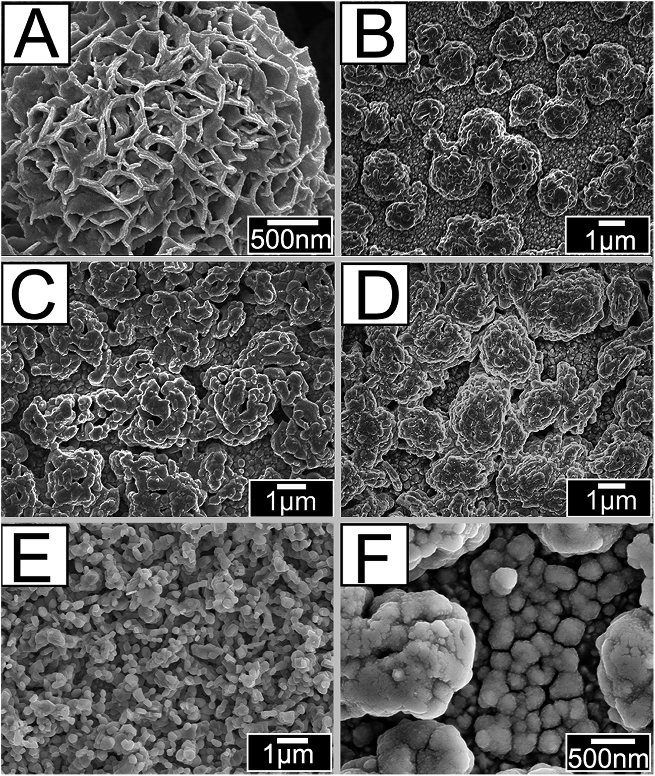 | ||
| Fig. 1 SEM patterns of: (A) the Bi2MoO6 before annealing, (B) BM-20, (C) BM-30, (D) BM-40, (E) CdS, and (F) Bi2MoO6 & CdS composites. | ||
With a view to further investigating CdS nanoparticles located in the composite, energy-dispersive spectroscopy (EDS) was employed and the results of different points of Bi2MoO6 & CdS composite are shown in Fig. 2. The different elements and their contents can be clearly seen in Fig. 2. Because the contents of O and S were significantly decreased in the upper layer, it can be inferred that only a portion of CdS was deposited onto the surface of Bi2MoO6. Correspondingly, in the lower layer, no Bi and Mo elements were observed and the S and Cd element signals were significantly high, which clearly indicated that these were from CdS nanoparticles. The Si elements were from the FTO glass under high testing energy. As a result, it can be reasonably speculated that a portion of CdS was deposited onto the surface of Bi2MoO6 and another portion of CdS was deposited onto the FTO.
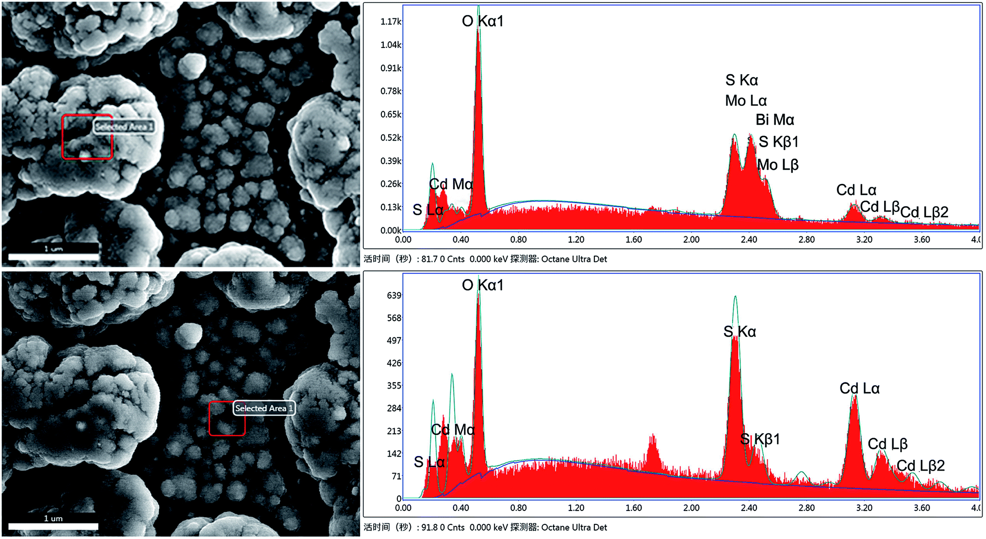 | ||
| Fig. 2 The EDX patterns of Bi2MoO6 & CdS composites. | ||
The X-ray diffraction (XRD) patterns of the BM-20, BM-30, BM-40, and Bi2MoO6 & CdS composite photoanodes are exhibited in Fig. 3. It is clearly shown that the diffraction peaks were well indexed to Bi2MO6 (JCPDS 21-0102); namely, the characteristic sharp peaks could be indexed to the (111), (131), (200), (202), and (133) crystal faces at 23.524, 28.264, 46.707, and 55.538. Furthermore, we observed the exposed (131) crystal faces were different with the different precursor contents; particularly, the BM-30 displayed maximal intensity of (131) crystal faces, exhibiting the best catalytic activity of current density at 0.38 mA cm−2. The diffraction peaks of CdS were not observed; because of its low content in the composite, the CdS diffraction peaks are inconspicuous. In addition, the patterns have distinct diffraction peaks at 26.5, 37.7, 51.7, 61.7, and 65.7, which could be indexed to the SnO2 structure on the FTO.
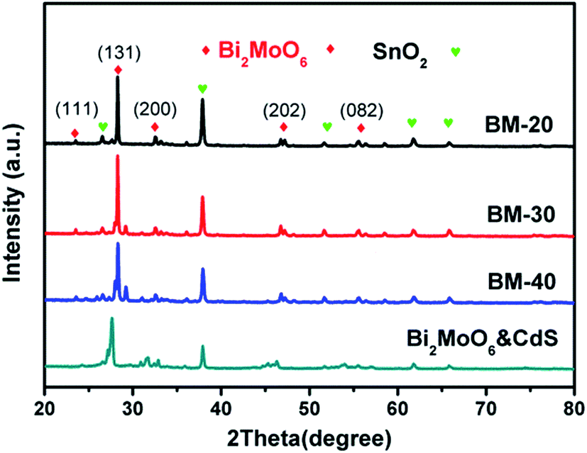 | ||
| Fig. 3 XRD patterns of the BM-20, BM-30, BM-40, and Bi2MoO6 & CdS composite photoanodes samples. | ||
3.2 The element composition of Bi2MoO6 & CdS composite photoanodes sample
To determine chemical composition and identify chemical states of the elements in the Bi2MoO6 & CdS composite photoanode sample, X-ray photoelectron spectroscopy (XPS) spectra are also presented in Fig. 4. Specifically, Fig. 4A is a survey spectrum of the Bi2MoO6 & CdS composite photoanode, which demonstrates that elements of Bi, Mo, O, Cd, and S exist in the Bi2MoO6 & CdS composite photoanode. In Fig. 4B the binding energies 157.8 and 163.1 eV correspond to Bi 4f7/2 and Bi 4f5/2, respectively.31–33 For the XPS spectrum of S 2p in Fig. 4B, the peak located at 160.5 was assigned to S 2p3/2 and another one located at 162.6 corresponded to S 2p1/2. In Fig. 4C, the binding energies of around 232.2 eV and 235.3 eV could be ascribed to Mo 3d.34 The two peaks centered at 405.5 eV and 412.2 eV in the Cd 3d XPS spectrum (Fig. 4D) are ascribed to the Cd 3d5/2 and Cd 3d3/2, respectively.35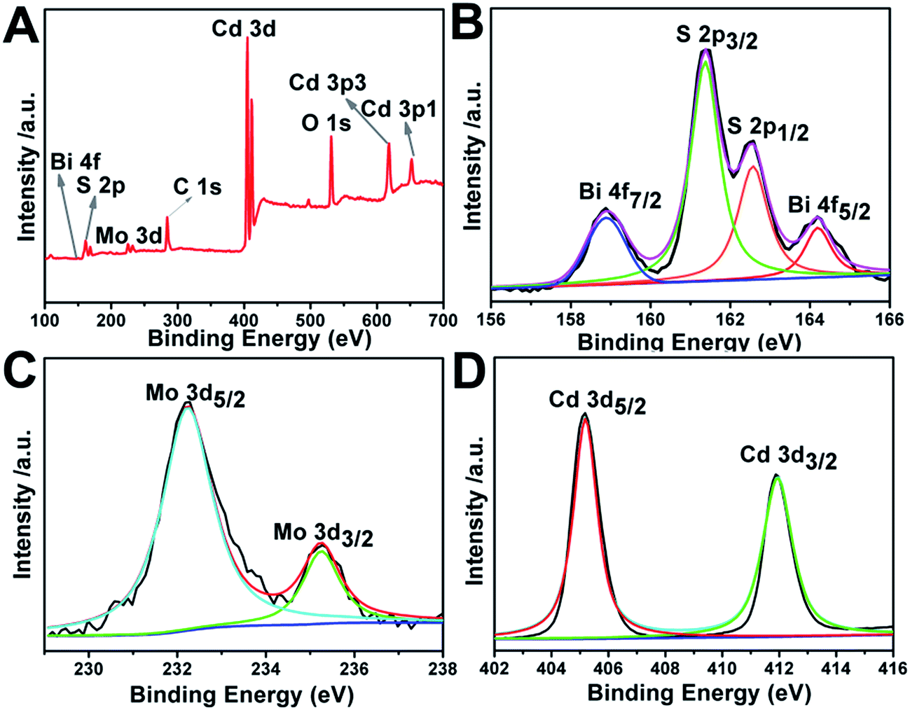 | ||
| Fig. 4 The X-ray photoelectron spectroscopy (XPS) spectra of Bi2MoO6 & CdS composite photoanode. | ||
3.3 UV-vis absorption spectra
Three samples, namely Bi2MoO6, CdS, and Bi2MoO6 & CdS photoanodes, were employed. The sample of pure Bi2MoO6 was prepared with Bi(NO3)3 as the precursor and the mole content is 30 mM. The Bi2MoO6 & CdS photoanode agreed with the XPS sample's data.UV-vis light absorption spectra of pure Bi2MoO6, CdS, and Bi2MoO6 & CdS photoanodes are shown in Fig. 5A, respectively. It can be clearly seen that absorption of the pure Bi2MoO6 photoelectrode was 450 nm, the pure CdS photoelectrode was 500 nm, and the Bi2MoO6 & CdS composite photoelectrode was 490 nm. The UV-vis DRS of the Bi2MoO6 & CdS composite photoelectrode has an obviously red shift compared to pure Bi2MoO6. In addition, the band gap of CdS and Bi2MoO6 was calculated in Fig. 5B. Specifically, the band gap of CdS was 2.46 eV and Bi2MoO6 was 2.73, which was beneficial to photocatalytic excitation by visible light. This suggested that the as-fabricated Bi2MoO6 & CdS composite photoelectrode had a suitable band gap. Therefore, good PEC properties of the Bi2MoO6 & CdS composite photoelectrode under solar irradiation are presented.
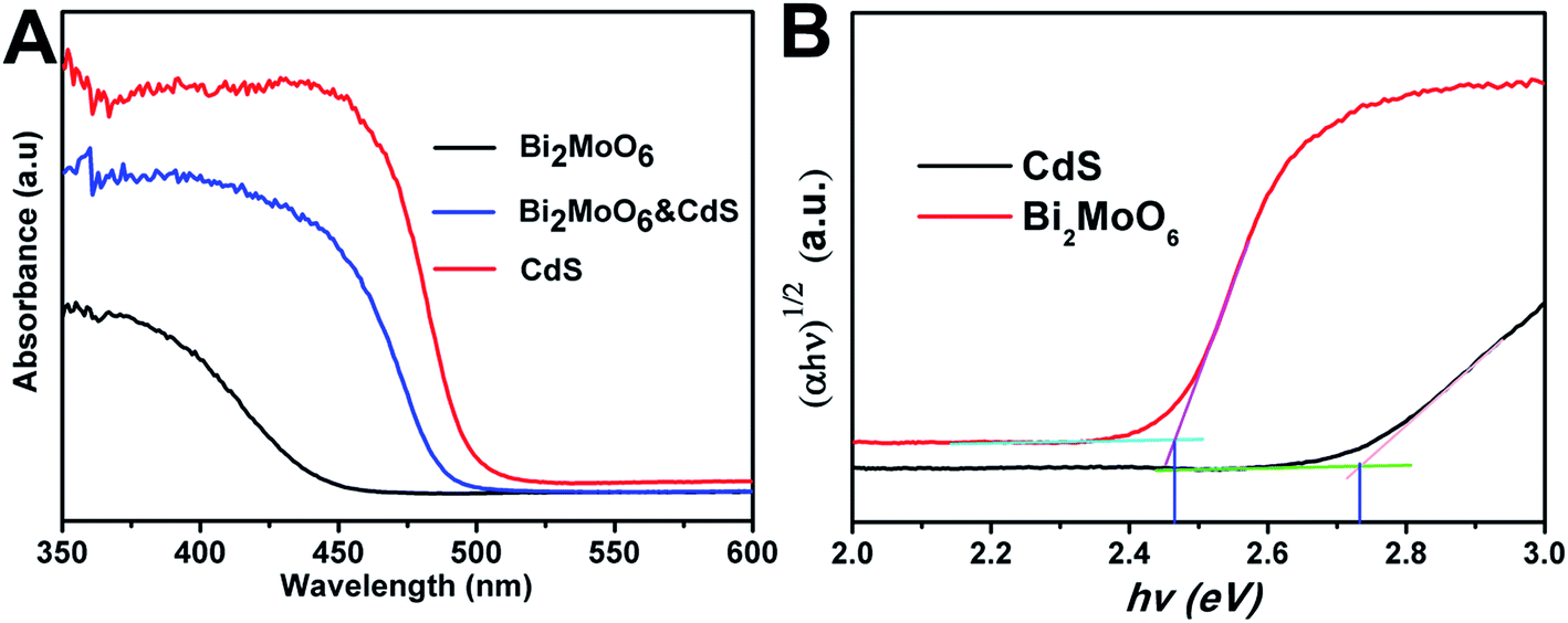 | ||
| Fig. 5 (A) The UV-vis absorption spectra of the Bi2MoO6, CdS, and Bi2MoO6 & CdS electrodes; (B) the band gap of CdS and Bi2MoO6. | ||
3.4 The photoelectrochemical properties
The photoelectrochemical properties of BM-20, BM-30, BM-40, and Bi2MoO6 & CdS composite photoanode were investigated. Specifically, an experiment was carried out in 0.2 M Na2SO4 under illumination of 100 mW cm−2 coupled with an AM 1.5 filter to provide simulated solar irradiation. The linear-sweep voltammograms under transient illumination are presented in Fig. 6A, from which it can be seen that the composite electrodes of Bi2MoO6 & CdS have a much lower photocurrent onset potential than the pure Bi2MoO6. This is mainly because of the extended absorption edges of the Bi2MoO6 photoelectrode resulting from the loaded CdS. Furthermore, pure CdS presented an abnormal decline following potential augmenting because pure CdS has a serious light corrosion. Fig. 6B shows amperometric I–t curves of pure CdS, BM-20, BM-30, BM-40, and Bi2MO6 & CdS composite photoanodes. The current density of pure CdS rapidly descended with irradiation time while pure Bi2MoO6 BM-40 displayed maximum photocurrent density (0.38 mA cm−2) at a potential of 0.6 V vs. RHE for 0.2 M Na2SO4. The Bi2MoO6 & CdS composite photoanode exhibited the highest photocurrent density (0.86 mA cm−2) under the same conditions. When CdS was added to the pure Bi2MoO6 photoanode, it extended the absorption edges as well as providing more active sites, which facilitated the photoanode taking advantage of the wider light irradiation and photogenerated charges carriers. Meanwhile, Bi2MoO6 could carry photogenerated charges of CdS away over time so that CdS light corrosion was inhibited. Therefore, the Bi2MoO6 & CdS composite electrode remarkably enhanced the photocurrent property.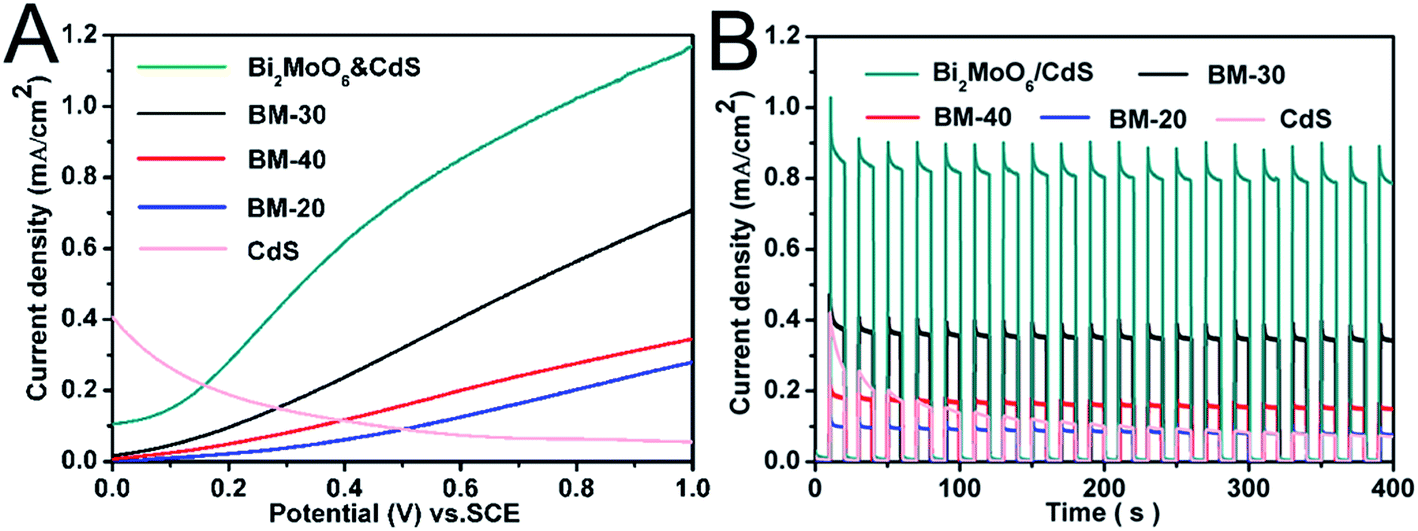 | ||
| Fig. 6 (A) Linear sweep voltammograms of BM-20, BM-30, BM-40, and Bi2MO6 & CdS composite photoanode samples in visible light illumination (100 mW cm−2); (B) amperometric I–t curves of BM-20, BM-30, BM-40, and Bi2MO6 & CdS composite photoanodes samples. | ||
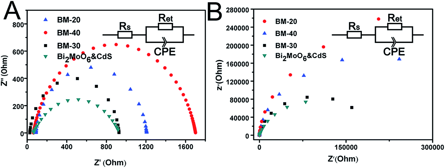
The interfacial charge transfer on the electrode can be characterized by Electrochemical Impedance Spectroscopy (EIS) shown in Fig. 7. The interfacial charge transfer resistance (Rct) can be represented by the diameter of the semicircle in a Nyquist plot. It can be clearly seen that the Rct under illumination (Fig. 7A) is lower than that in the dark (Fig. 7B), which suggests a fast interfacial charge transfer upon illumination. The diameter of Bi2MoO6 & CdS semicircle is smaller than that of pure Bi2MoO6, proving that the decoration of CdS facilitated the charge transfer process due to a type II band alignment between Bi2MoO6 and CdS.
 | ||
| Fig. 7 Electrochemical impedance spectroscopy (EIS) Nyquist plots of BM-20, BM-30, BM-40, and Bi2MoO6 & CdS composite photoanodes samples. | ||
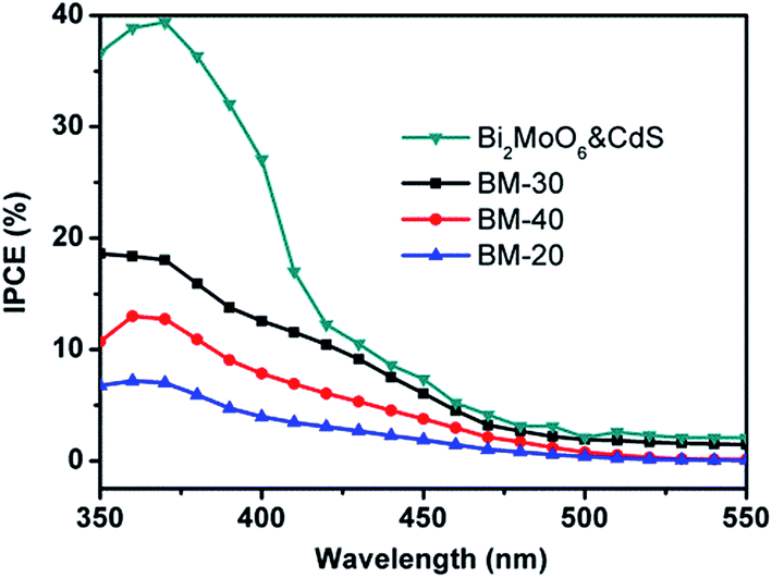
Fig. 8 shows measurements of the incident photon-to-current conversion efficiency (IPCE) of Z BM-20, BM-30, BM-40, and Bi2MoO6 & CdS.
 | ||
| Fig. 8 The incident photon-to-current conversion efficiency (IPCE) of BM-20, BM-30, BM-40, and Bi2MoO6 & CdS. | ||
IPCE was calculated as follows:19,27,36
 | (1) |
4. Conclusion
In summary, since most Bi-based photoelectrodes have suitable band gaps and can effectively promote hydrogen evolution from water splitting, a novel Bi2MoO6 thin film photoanode was prepared by growing Bi2MoO6 on an electrical substrate directly via an in situ process. The photoanodes show well-shaped thin film morphologies and exhibit impressive photoelectrochemical properties compared to Bi-based photoanodes synthesized by conventional methods. Particularly, the morphology of our thin film photoanodes can be controlled by precursor content. Crystal structure and morphology was carefully studied with SEM, XPS, UV-vis diffuse reflectance, and PEC performance etc., and the results are in good agreement with each other.The Bi2MoO6 thin film photoanodes possess long-term stability under solar irradiation and show a considerable photocurrent. The results of our photoelectron studies proved that the precursor Bi(NO3)3 mole fraction with 30 mM can reach a maximal photocurrent of 0.38 mA cm−2. In addition, we further enhanced the Bi2MoO6 thin film photoanodes photocurrent after CdS modifying the thin film electrodes, the photocurrent of which doubled in comparison with the primary Bi2MoO6 (about 0.85 mA cm−2) under the identical conditions. We believe that this facile method may be suitable for synthesizing nanostructured Bi2MoO6-based materials for use in solar energy devices.
Acknowledgements
This work was financially supported by the Chinese National Natural Science Foundation (21603274, 41663012, 21263001 and 21463001).References
- J. Zhang, T. Wang, X. Chang, A. Li and J. Gong, Fabrication of porous nanoflake BiMOx (M = W, V, and Mo) photoanodes via hydrothermal anion exchange, Chem. Sci., 2016, 7(10), 6381–6386 RSC.
- M. Dasog, J. Kehrle, B. Rieger and J. G. Veinot, Silicon Nanocrystals and Silicon–Polymer Hybrids: Synthesis, Surface Engineering, and Applications, Angew. Chem., Int. Ed., 2016, 55(7), 2322–2339 CrossRef CAS PubMed.
- S. Kawasaki, R. Takahashi, T. Yamamoto, M. Kobayashi, H. Kumigashira, J. Yoshinobu and M. Lippmaa, Photoelectrochemical water splitting enhanced by self-assembled metal nanopillars embedded in an oxide semiconductor photoelectrode, Nat. Commun., 2016, 7, 11818 CrossRef CAS PubMed.
- X. Liu, G. Dong, S. Li, G. Lu and Y. Bi, Direct observation of charge separation on anatase TiO2 crystals with selectively etched {001} facets, J. Am. Chem. Soc., 2016, 138, 2917–2920 CrossRef CAS PubMed.
- F. E. Osterloh, Inorganic materials as catalysts for photochemical splitting of water, Chem. Mater., 2007, 20(1), 35–54 CrossRef.
- J. Manassen, D. Cahen and G. Hodes, Electrochemical, solid state, photochemical and technological aspects of photoelectrochemical energy converters, Nature, 1976, 263, 97–100 CrossRef CAS.
- H. Zhang, X. Liu, Y. Li, Q. Sun, Y. Wang, B. J. Wood and H. Zhao, Vertically aligned nanorod-like rutile TiO2 single crystal nanowire bundles with superior electron transport and photoelectrocatalytic properties, J. Mater. Chem., 2012, 22(6), 2465–2472 RSC.
- R. Abe, Recent progress on photocatalytic and photoelectrochemical water splitting under visible light irradiation, J. Photochem. Photobiol., C, 2010, 11(4), 179–209 CrossRef CAS.
- K. S. Joya, Y. F. Joya, K. Ocakoglu and R. van de Krol, Water-Splitting Catalysis and Solar Fuel Devices: Artificial Leaves on the Move, Angew. Chem., Int. Ed., 2013, 52(40), 10426–10437 CrossRef CAS PubMed.
- M. G. Walter, E. L. Warren, J. R. McKone, S. W. Boettcher, Q. Mi, E. A. Santori and N. S. Lewis, Solar water splitting cells, Chem. Rev., 2010, 110(11), 6446–6473 CrossRef CAS PubMed.
- D. Li, Z. Xing, X. Yu and X. Cheng, One-step hydrothermal synthesis of C–N–S-tri doped TiO2-based nanosheets photoelectrode for enhanced photoelectrocatalytic performance and mechanism, Electrochim. Acta, 2015, 170, 182–190 CrossRef CAS.
- X. Cheng, G. Pan and X. Yu, Visible Light Responsive Photoassisted Electrocatalytic System Based on CdS NCs Decorated TiO2 Nano-tube Photoanode and Activated Carbon Containing Cathode for Wastewater Treatment, Electrochim. Acta, 2015, 156, 94–101 CrossRef CAS.
- Y. Wang, S. Ge, L. Zhang, J. Yu, M. Yan and J. Huang, Visible photoelectrochemical sensing platform by in situ generated CdS quantum dots decorated branched-TiO2 nanorods equipped with Prussian blue electrochromic display, Biosens. Bioelectron., 2016, 859–865 Search PubMed.
- S. Yuan, J. Mu, R. Mao, Y. Li, Q. Zhang and H. Wang, All-nanoparticle self-assembly ZnO/TiO2 heterojunction thin films with remarkably enhanced photoelectrochemical activity, ACS Appl. Mater. Interfaces, 2014, 6(8), 5719–5725 CAS.
- Y. Bi, B. Jin and Z. Jiao, Efficient charge separation between Bi2MoO6 nanosheets and ZnO nanowires for enhanced photoelectrochemical properties, J. Mater. Chem. A, 2015, 3(39), 19702–19705 Search PubMed.
- T. Wang, B. Jin, Z. Jiao, G. Lu, J. Ye and Y. Bi, Electric field-directed growth and photoelectrochemical properties of cross-linked Au–ZnO hetero-nanowire arrays, Chem. Commun., 2015, 51(11), 2103–2106 RSC.
- L. J. Di, H. Yang, G. Hu, T. Xian, J. Y. Ma, J. L. Jiang, R. S. Li and Z. Q. Wei, Enhanced photocatalytic activity of BiFeO3 particles by surface decoration with Ag nanoparticles, J. Mater. Sci.: Mater. Electron., 2014, 25(6), 2463–2469 CrossRef CAS.
- X. Xu, Y. H. Lin, P. Li, L. Shu and C. W. Nan, Synthesis and photocatalytic behaviors of high surface area BiFeO3 thin films, J. Am. Ceram. Soc., 2011, 94(8), 2296–2299 CrossRef CAS.
- S. J. Moniz, C. S. Blackman, P. Southern, P. M. Weaver, J. Tang and C. J. Carmalt, Visible-light driven water splitting over BiFeO3 photoanodes grown via the LPCVD reaction of [Bi(OtBu)3] and [Fe(OtBu)3]2 and enhanced with a surface nickel oxygen evolution catalyst, Nanoscale, 2015, 7(39), 16343–16353 RSC.
- X. Zhao, Y. Wu, W. Yao and Y. Zhu, Photoelectrochemical properties of thin Bi2WO6, films, Thin Solid Films, 2007, 515(11), 4753–4757 CrossRef CAS.
- H. He, S. Berglund, A. E. Rettie, W. Chemelewski, P. Xiao and Y. Zhang, et al., Synthesis of BiVO4 nanoflake array films for photoelectrochemical water oxidation, J. Mater. Chem. A, 2014, 2(24), 9371–9379 CAS.
- C. Ng, A. Iwase, Y. H. Ng and R. Amal, Transforming anodized WO3 films into visible-light-active Bi2WO6 photoelectrodes by hydrothermal treatment, J. Phys. Chem. Lett., 2012, 3(7), 913–918 CrossRef CAS PubMed.
- S. N. Lou, J. Scott, A. Iwase, R. Amal and Y. H. Ng, Photoelectrochemical water oxidation using a Bi2MoO6/MO3 heterojunction photoanode synthesised by hydrothermal treatment of an anodised MoO3 thin film, J. Mater. Chem. A, 2016, 4(18), 6964–6971 CAS.
- Y. Ma, Y. Jia, L. Wang, M. Yang, Y. Bi and Y. Qi, Efficient Charge Separation between Bi and Bi2MoO6 for Photoelectrochemical Properties, Chem.–Eur. J., 2016, 22(17), 5844–5848 CrossRef CAS PubMed.
- Y. Wu, C. Chen, Y. Huang, W. Lin, Y. Yen and C. Lu, Pirimicarb degradation by BiVO4 photocatalysis: parameter and reaction pathway investigations, Sep. Sci. Technol., 2016, 51(13), 2284–2296 CrossRef CAS.
- T. W. Kim and K. S. Choi, Improving stability and photoelectrochemical performance of BiVO4 photoanodes in basic media by adding a ZnFe2O4 layer, J. Phys. Chem. Lett., 2016, 7(3), 447–451 CrossRef CAS PubMed.
- C. Feng, Z. Jiao, S. Li, Y. Zhang and Y. Bi, Facile fabrication of BiVO4 nanofilms with controlled pore size and their photoelectrochemical performances, Nanoscale, 2015, 7(48), 20374–20379 RSC.
- M. Long, W. Cai and H. Kisch, Photoelectrochemical properties of nanocrystalline Aurivillius phase Bi2MoO6 film under visible light irradiation, Chem. Phys. Lett., 2008, 461(1), 102–105 CrossRef CAS.
- X. Zhao, J. Qu, H. Liu and C. Hu, Photoelectrocatalytic degradation of triazine-containing azo dyes at γ-Bi2MoO6 film electrode under visible light irradiation (λ > 420 nm), Environ. Sci. Technol., 2007, 41(19), 6802–6807 CrossRef CAS PubMed.
- X. Zhao, T. Xu, W. Yao and Y. Zhu, Synthesis and photoelectrochemical properties of thin bismuth molybdates film with various crystal phases, Thin Solid Films, 2009, 517(20), 5813–5818 CrossRef CAS.
- X. Ding, W. Ho, J. Shang and L. Zhang, Self doping promoted photocatalytic removal of no under visible light with Bi2MoO6: indispensable role of superoxide ions, Appl. Catal., B, 2016, 182, 316–325 CrossRef CAS.
- G. Tian, Y. Chen, J. Zhou, C. Tian, R. Li, C. Wang and H. Fu, In situ growth of Bi2MoO6 on reduced graphene oxide nanosheets for improved visible-light photocatalytic activity, CrystEngComm, 2014, 16(5), 842–849 RSC.
- Z. Zhao, W. Zhang, Y. Sun, J. Yu, Y. Zhang, H. Yan and Z. Wu, Bi Cocatalyst/Bi2MoO6 Microspheres Nanohybrid with SPR-Promoted Visible-Light Photocatalysis, J. Phys. Chem. C, 2016, 11889–11898 CAS.
- M. Zhang, C. Shao, J. Mu, Z. Zhang, Z. Guo, P. Zhang and Y. Liu, One-dimensional Bi2MoO6/TiO2 hierarchical heterostructures with enhanced photocatalytic activity, CrystEngComm, 2012, 14(2), 605–612 RSC.
- S. Cao, X. Yan, Z. Kang, Q. Liang, X. Liao and Y. Zhang, Band alignment engineering for improved performance and stability of ZnFe2O4 modified CdS/ZnO nanostructured photoanode for PEC water splitting, Nano Energy, 2016, 24, 25–31 CrossRef CAS.
- K. P. S. Parmar, H. J. Kang, A. Bist, P. Dua, J. S. Jang and J. S. Lee, Photocatalytic and Photoelectrochemical Water Oxidation over Metal Doped Monoclinic BiVO4 Photoanodes, ChemSusChem, 2012, 5(10), 1926–1934 CrossRef CAS PubMed.
| This journal is © The Royal Society of Chemistry 2017 |