
 Open Access Article
 This Open Access Article is licensed under a Creative Commons Attribution-Non Commercial 3.0 Unported Licence
Intramolecular oxidative cyclodehydrogenation route for the synthesis of strap-like conjugated polymers†
Junwei Yanga,
Wei Huanga,
Tingting Linb,
Xiaoyong Panb,
Haoyun Zhua,
Yuli Huanga and
Weizhi Wang *a
*a
aState Key Laboratory of Molecular Engineering of Polymers, Department of Macromolecular Science, Collaborative Innovation Center of Polymers and Polymer Composite Materials, Fudan University, Shanghai 200433, P. R. China. E-mail: weizhiwang@fudan.edu.cn
bInstitute of Materials Research and Engineering, A*STAR (Agency for Science, Technology and Research), 2 Fusionopolis Way, Innovis, #08-03, Singapore 138634, Singapore
First published on 8th February 2017
Abstract
Strap-like conjugated polymers, as the promising materials with opening band gaps, are being rapidly developed for future electronic devices. A bottom-up solution-based synthesis of two novel narrow strap-like polymers on the nanometer scale was successfully achieved by intramolecular oxidative cyclodehydrogenation, and two synthesized polymer precursors were converted via palladium-catalyzed Suzuki–Miyaura polymerization. In comparison, the strap-like polymer, which has more extended conjugation, exhibits better electron transmission and planarization owing to its greater electron delocalization. Owing to their excellent thermal stability and conducting properties, these structurally well-defined nanoribbons were utilized in top-gate field-effect transistors via direct solution processing. The fabricated devices could function well in lower-voltage operations (<5 V) and displayed high performance, with mobilities of about 0.38 cm2 V−1 s−1 at an on–off ratio of 3.67 × 10³ and 0.48 cm2 V−1 s−1 at an on–off ratio of 6.25 × 10³.
Introduction
As a two-dimensional material, graphene has been studied and rapidly developed since the first single-layer graphene was successfully exfoliated from graphite.1–6 Numerous exceptional properties of graphene have been found by researchers in subsequent years.7–11 Among these, its excellent charge carrier mobility enables graphene to be a promising material for nanoelectronics applications. However, it is impossible to directly utilize pristine graphene with a zero band gap in practical devices.12–14 Thus, it is crucial to discover a way of opening the band gap to fabricate devices such as field-effect transistors (FETs).15–17 Many groups have investigated a variety of approaches, such as altering the concentration of the carrier in bilayer graphene,18 applying uniaxial strain in a graphene layer,19 and the programmed adsorption of hydrogen onto graphene surfaces, for introducing a band gap into graphene.20,21 However, the most straightforward method of opening tunable band gaps is to break the geometric structure of graphene into nanometer-wide confined strips, the best-known of which are referred to as graphene nanoribbons (GNRs).22,23GNRs have attracted the attention of many scientists in physics, chemistry and materials science owing to their fascinating optoelectronic properties and extensive potential in nanoelectronics applications.24,25 There are two principal approaches to the synthesis of GNRs, namely, “top-down” and “bottom-up” approaches. A wide variety of top-down techniques such as cutting graphene on a surface,26 catalysis by metal nanoparticles, lithography,27,28 sonochemical extraction from expanded graphite,29 plasma etching with a protected polymer, or unzipping carbon nanotubes30,31 have commonly been used to tailor GNRs. GNRs prepared by top-down methods exhibit controllable sizes and good transport properties.32 Their low yield is a weakness of top-down methods; some so-called “high-quality” GNRs have yields of only around 2%.33,34 In contrast, bottom-up chemical synthesis provides another approach to obtain structurally well-defined and atomically precise GNRs.35 For instance, several methods such as chemical vapor deposition from one-dimensional templates,36 decomposition of molecules inside carbon nanotubes,37 and surface-assisted cyclodehydrogenation reactions38 can produce structurally outstanding GNRs with uniform lateral structures. Nevertheless, most of these established methods have low efficiency and product yield. Müllen et al. developed an efficient way of using solution-mediated synthesis to yield GNRs with a tailored band gap and atomically precise edges.39 In addition, the derived GNRs prepared by this method can be efficiently transferred onto dielectric surfaces for the further fabrication of FETs. Normally, there are three major steps involved in bottom-up solution-mediated synthesis. The first is the design of appropriate molecular precursors, the next is solution polymerization of the molecular precursors, and the last is intramolecular cyclodehydrogenation via the Scholl reaction.40 As far as we know, comparative studies of polymer precursors for GNRs mostly focus on polyphenylene, which has been employed to produce GNRs with different edge structures and aspect ratios. Kyung et al. studied a series of graphene nanoribbons of various widths containing phenylene, naphthalene and anthracene units.41 There are several studies that mention tetraphenylethene (TPE), which exhibits interesting chemical and physical properties.42,43 In one of our previous works,44 a series of graphene-like molecules based on TPE with various degrees of planarity were synthesized. This is a facile and highly efficient cyclization reaction using anhydrous iron(III)chloride (FeCl3) as an oxidant.45,46 Inspired by the above studies, we proposed to prepare structurally defined strap-like polymers of different widths from designed polymer precursors combining phenylene, naphthalene and TPE units.
In this work, (Z)-1,2-bis(4-tert-butylphenyl)-1,2-bis(4,4,5,5-tetramethyl-1,3,2-dioxaborolan-2-yl)ethene was synthesized as one monomer. The alkyl chains on the benzene rings were selected to make the target polymers display excellent solubility in common organic solvents and possess a larger molecular weight. Dibromobenzene and dibromonaphthalene were added as the other monomers to incorporate benzene and naphthalene rings, respectively, into the backbones of the tailor-made polymer precursors (PTVB and PTVN). Then, two similar strap-like polymers on the nanometer scale of slightly different widths and degrees of conjugation were produced by oxidative cyclodehydrogenation (OPTVB and OPTVN). The efficient planarization of the strap-like polymers from the precursors was corroborated by various measurements, which showed similar properties to those of GNRs. Furthermore, the synthesized strap-like polymers were used as active semiconductor layers to fabricate thin-film FETs by direct solution processing. These devices containing graphene-like nanoribbons could function well at a low gate voltage and exhibited typical p-type transport behavior with excellent charge carrier mobility and on–off current ratio, which suggested extensive potential for FETs.
Experimental section
Materials and instruments
All the reagents and chemicals used were purchased from Aldrich or Sinopharm Chemical Reagent Company. Tetrahydrofuran (THF) and toluene both distilled over small sodium wires and benzophenone were added under nitrogen (N2) immediately prior to use, and N,N-dimethylformamide (DMF), which was used without purification, was of high-pressure liquid chromatography grade.Gel permeation chromatography (GPC) measurements were recorded with an Agilent/Wyatt 1260 gel permeation chromatograph. Calibration was performed by employing commercially available polystyrene. 1H and 13C nuclear magnetic resonance spectra (NMR) were recorded with a Bruker AVANCE III HD 400 MHz FT-NMR spectrometer in deuterated dichloromethane (CD2Cl2) and 1,1,2,2-tetrachloroethane (C2D2Cl4). Chemical shifts are given in ppm units using tetramethylsilane (TMS; δ = 0) as an internal standard. Thermogravimetric analysis (TGA) measurements were made using a PerkinElmer Pyris 1 thermogravimetric analyzer by heating from 50 °C to 765 °C at a heating rate of 10 °C min−1 under a dry N2 flow. Differential scanning calorimetry (DSC) measurements were conducted with a TA Q2000 differential scanning calorimeter over one heating–cooling cycle from 50 °C to 270 °C at a ramp rate of 10 °C min−1 under a constant N2 flow. Powder X-ray diffraction (XRD) patterns were obtained using an X'Pert Pro MPD diffractometer with Cu Kα radiation (λ = 1.5418 Å) at 25 °C (scan ranges: 3–30° and 3–50°). A PerkinElmer Lambda 750 UV-visible spectrophotometer was employed for UV spectra in a THF solution. Infrared spectra were recorded with KBr pellets using a Thermo Fisher Nicolet 6700 Fourier transform infrared (FTIR) spectrometer, where the percentage transmittance or absorbance was plotted vs. the wavenumber (in cm−1). Photoluminescence (PL) spectra were recorded in a THF solvent with a Photon Technology International, Inc., QM40 fluorescence lifetime spectrometer at room temperature. The PL quantum yields (ΦF) were estimated using fluorescein (ΦF = 92% in 0.1 M NaOH (aq)) as a standard. The PL lifetimes were measured using the same QM40 spectrometer by means of a time-corrected single-photon counting system at room temperature. Cyclic voltammetry (CV) was conducted on a T30/FRA2 electrochemical workstation. The product films were coated on a glassy carbon electrode with a cross-section of 0.08 cm2. Using ferrocene (4.8 eV under vacuum) as an internal standard, measurements were performed in an electrolyte of 0.1 M tetrabutylammonium hexafluorophosphate (TBAPF6) in acetonitrile at a scan rate of 100 mV s−1 at room temperature under the protection of N2. The reference electrode was an Ag/AgNO3 electrode, and a platinum wire was employed as the counter electrode. The samples were analyzed with an AB SCIEX 5800 matrix-assisted laser desorption/ionization time-of-flight mass spectrometer (MALDI-TOF) using trans-2-[3-(4-tert-butylphenyl)-2-methyl-2-propenylidene]malononitrile (DCTB) as the matrix. Elemental analysis was performed with a Vario EL3 instrument (Elementar, Germany). The entire X-ray crystallographic data were collected with a Bruker P4 diffractometer equipped with a rotating anode using graphite-monochromated Mo Kα radiation (λ = 0.71073 Å) and a Bruker SMART 1K CCD area detector (employing the SMART program). Data processing was implemented by means of the SAINT program, whereas the SADABS program was employed for scaling the diffraction data, an empirical absorption correction based on redundant reflections and the utilization of a decay correction. The final structures of the products were solved by utilizing the direct-methods procedure in the Bruker SHELXL program library and refined by the full-matrix least-squares approach on F2. All non-hydrogen atoms were refined using anisotropic thermal parameters.
Simultaneously, hydrogen atoms were combined as fixed contributors at calculated positions with isotropic thermal parameters based on the carbon atoms to which they were bonded. The morphological characterization of the synthesized products was performed with a TESCAN VEGA TS 5136MM variable-vacuum scanning electron microscope (SEM). Polarizing microscopy (POM) images were obtained with a DM2500P polarizing microscope at room temperature. Scanning tunneling microscopy (STM) was carried out with a Nanoscope IIIa instrument at the solid/liquid interface in 1-phenyloctane at room temperature [0.1 mM toluene solution on freshly cleaved highly oriented pyrolytic graphite (HOPG)]. A mechanically etched Pt/Ir (90![[thin space (1/6-em)]](https://www.rsc.org/images/entities/char_2009.gif) :10) wire was used as the STM tip. The instrument was operated in constant-current mode at a tunnelling current of 319 pA and a bias voltage of 610 mV. All periodic DFT calculations were performed using SIESTA code with numerical orbital basis sets. The exchange-correlation functional used was the generalized gradient approximation method with the help of the Gaussian 09 program package.
:10) wire was used as the STM tip. The instrument was operated in constant-current mode at a tunnelling current of 319 pA and a bias voltage of 610 mV. All periodic DFT calculations were performed using SIESTA code with numerical orbital basis sets. The exchange-correlation functional used was the generalized gradient approximation method with the help of the Gaussian 09 program package.
FET device fabrication
Commercially available highly p-doped SiO2 (300 nm)/Si wafers were washed with acetone and methanol, H2O2/H2SO4 and deionized water in turn. The conjugated polymers in THF solution (1 mg mL−1) were spin-coated on these clean SiO2/Si wafers at a rotation speed of 6000 rpm. The thin films used as the semiconductor were placed in a vacuum environment for a time to evaporate the surplus solvent. Gold drain and source electrodes with a thickness of 50 nm (the typical channel length was 0.6 mm, and the width was 1 mm) were vapor-deposited on the polymer thin film. An ion gel comprising a mixture of a triblock copolymer, namely, poly(styrene-block-methyl methacrylate-block-styrene) (PS–PMMA–PS; MPS = 4.5 kg mol−1, MPMMA = 12.7 kg mol−1, MW = 21.3 kg mol−1), and an ionic liquid, namely, 1-ethyl-3-methylimidazolium bis(trifluoromethylsulfonyl)imide, in solution in ethyl propionate was used as the top-gate dielectric. The weight ratio of the solvent, ionic liquid and polymer was maintained at 20:9.3:0.7. The prepared ionic solution was drop-cast to cover the surfaces of the polymer film and the drain and source electrodes. Then, the transistor channels were covered by a thin foil of Al (with a thickness of 0.03 mm) to act as the top-gate electrode. Finally, a thin gold wire was inserted into the gel films between the top-gate metal film and the channel as a reference electrode.
Synthesis procedures
:Cu:Pd = 3:2:1) to the solution. This reaction blend was heated under reflux for 6 h until it appeared pure on testing by thin-layer chromatography, the mixture was cooled down, and the filtrate after filtering was concentrated in a vacuum environment. Finally, the product was purified by column chromatography on silica gel to obtain monomer 1 as white crystals in a yield of 86.5%. 1H NMR (400 MHz, CD2Cl2), δ (TMS, ppm): 7.52–7.42 (m, 4H), 7.42–7.33 (m, 4H), 1.33 (s, 18H); 13C NMR (100 MHz, CD2Cl2), δ (TMS, ppm): 151.56, 151.55, 151.54, 151.53, 151.52, 151.52, 131.19, 131.18, 131.16, 125.43, 125.43, 120.36, 88.79, 34.69, 34.68, 34.68, 31.01, 30.95, 30.92. Anal. calcd for C22H26 (290.44): C, 90.90; H, 9.10; found: C, 91.01; H, 8.99.Results and discussion
Synthesis and characterization
To obtain the expected polymer precursors, (Z)-1,2-bis(4-tert-butylphenyl)-1,2-bis(4,4,5,5-tetramethyl-1,3,2-dioxaborolan-2-yl)ethene (2) was designed and synthesized as a monomer for subsequent Suzuki cross-coupling polymerization.47 The mass spectrum of 2 confirmed its successful synthesis (ESI Fig. S1†). The complete synthetic procedures of 2 and the polymers are clearly outlined in Scheme 1. Diphenylacetylene with tert-butyl substituents (1) was synthesized in good yield by a method in a previous work.48 The tert-butyl groups on the benzene rings effectively improve the solubility of the polymers in organic solvents, which is beneficial for solution processing and polymerization. Fortunately, pure single crystals of both 1 and 2 were isolated from their solution in CH2Cl2/n-hexane. Their accurate structures were also identified by X-ray crystallographic analysis (Fig. 1 and Table S1†).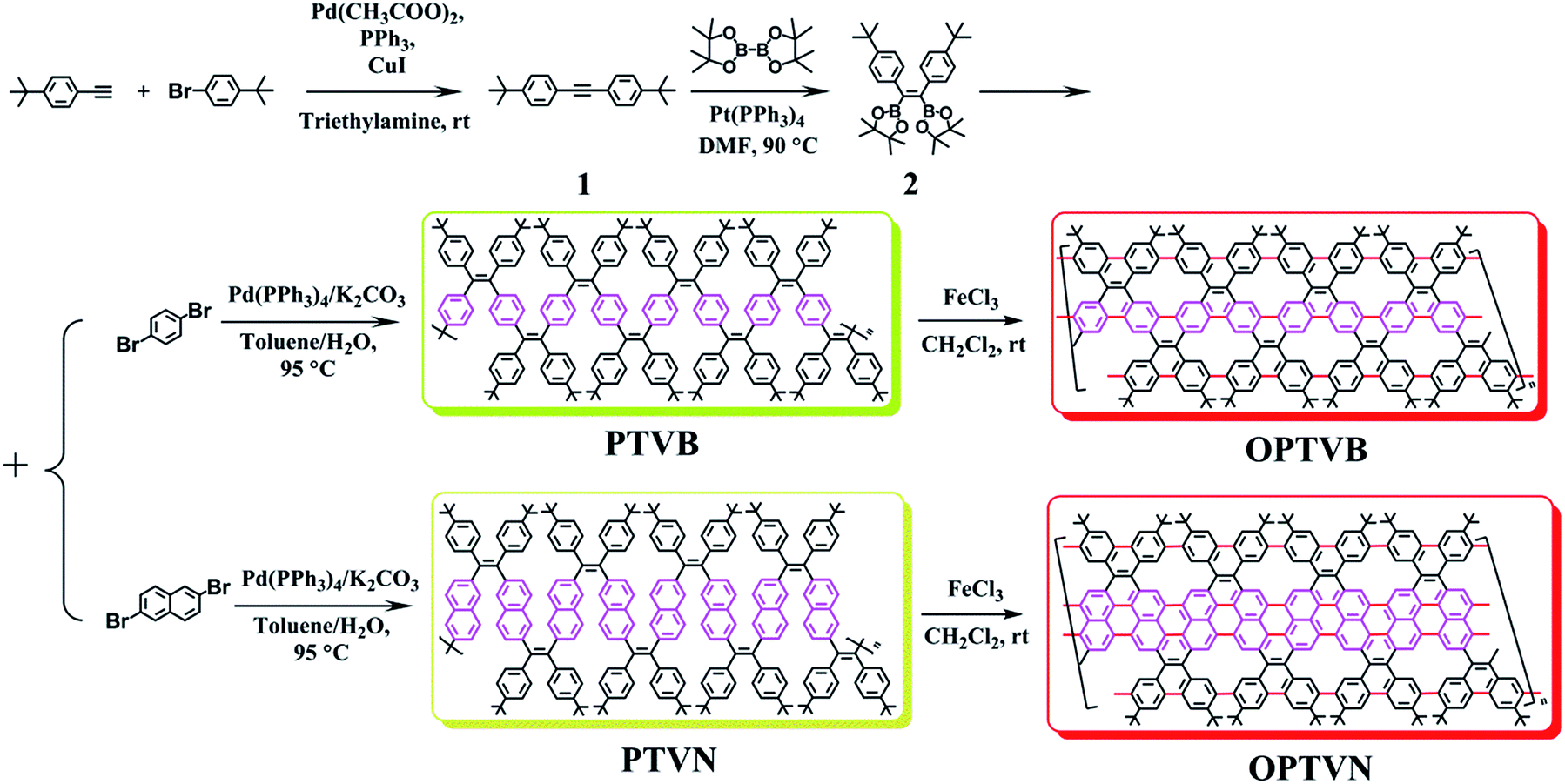 | ||
| Scheme 1 Procedures for the synthesis of the monomers (1 and 2) and polymers (PTVB, PTVN, OPTVB and OPTVN). | ||
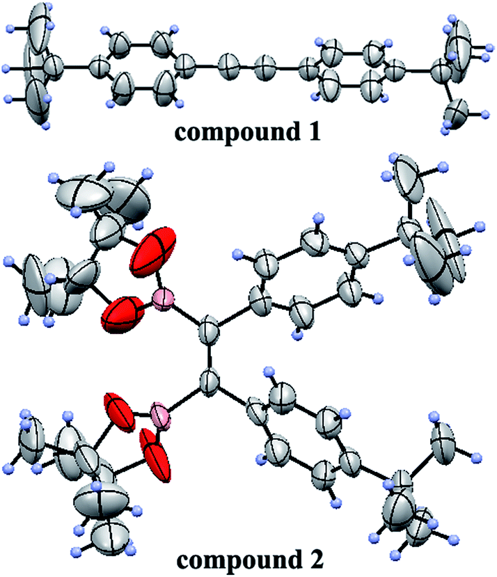 | ||
| Fig. 1 ORTEP drawings of 1 and 2. | ||
1,4-Dibromobenzene and 2,6-dibromonaphthalene were both purchased directly from reagent companies. On the last day of polymerization, there were precipitates that emitted fluorescence in the reaction solution, which indicated products of a high molecular weight. GPC measurements with THF as the eluent were in accordance with expectations (ESI Fig. S2†). The values of the number-average molecular weight (Mn) of PTVB and PTVN were 21.1 kg mol−1 and 17.3 kg mol−1, respectively. Furthermore, after being repeatedly precipitated in methanol they possessed narrow polydispersity indices (PDIs) calculated in terms of Mw/Mn of 1.10 and 1.13, respectively. Their high molecular weight and narrow PDIs enabled them to form good-quality films, which was favorable for subsequent device fabrication.
To prepare strap-like polymers with greater planarization, anhydrous FeCl3 was utilized as an oxidant for one-step oxidative cyclodehydrogenation. This reaction has been regularly used for the synthesis of polycyclic aromatic hydrocarbons owing to its absence of several drawbacks such as chlorination, dealkylation, or even migration of the alkyl substituents.49 At the end of the reaction, the remaining additional FeCl3 was consumed by pouring in an amount of methanol. The final cyclized products (OPTVB and OPTVN) both proved to be crimson powders. Although the steric hindrance of the bulky tert-butyl groups and the inner hydrogen atoms of the newly formed [14]annulene might hinder perfect cyclodehydrogenation,50 sufficient oxidation time made it possible to synthesize the cyclized products. The formation of the target strap-like polymers with extended planarization was confirmed by various characterizations.
All the prepared products were carefully purified and then characterized by 1H and 13C NMR. All their detailed spectra are included in the ESI Fig. S3–S12† to prove the successful syntheses of the compounds.
Here, Fig. 2a shows the 1H NMR spectra of PTVB and OPTVB as an example. Obviously, the peaks representing the protons on the phenyl rings merged into two broad peaks and weakened drastically after cyclodehydrogenation, which indicated that the formation of C–C bonds between the phenyl rings increased the degree of conjugation. This phenomenon was a major obstacle to detecting the corresponding aromatic protons. Therefore, variable-temperature 1H NMR analysis (25 °C to 120 °C) of OPTVB in C2D2Cl4 was carried out, as depicted in Fig. 2b. The peak at around 1.5 ppm was assigned to the resonance of protons in the tert-butyl groups. The signals that were unchanged at different temperatures showed that the chemical shifts of the aromatic resonances were independent of temperature; therefore, this was not attributed to the aggregation of OPTVB. The 1H NMR spectra of PTVN and OPTVN (ESI Fig. S9 and S11†) displayed a similar phenomenon, and the variable-temperature 1H NMR spectra of OPTVN exhibited the same situation as well (ESI Fig. S13†). Actually, this special phenomenon occurs widely in the field of conjugated carbon materials. However, it is unfortunate that a reliable and reasonable explanation of this phenomenon is still lacking.51
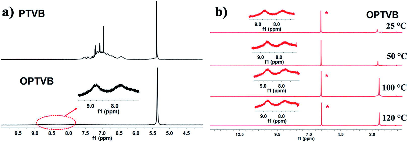 | ||
| Fig. 2 (a) 1H NMR spectra of PTVB and OPTVB in CD2Cl2; (b) 1H NMR spectra of OPTVB at varying temperatures (25–120 °C) in C2D2Cl4. The inset spectra are magnifications of the aromatic region. | ||
FTIR characterization
In addition to the NMR measurements, intramolecular cyclodehydrogenation was further confirmed by a comparison of the results of FTIR spectroscopic analysis between the precursors and dehydrogenated polymers. In Fig. 3a and b, within the middle infrared region the noticeable disappearance of the signal triad of aromatic C–H stretching vibrations at 3025, 3058, and 3082 cm−1 and the strong attenuation of the peaks corresponding to out-of-plane C–H deformation in the fingerprint regions representing mono- and disubstituted benzene rings at 698, 796, and 894 cm−1 both confirm efficient conversion from polymer precursors into straps. In addition, another combination peak within the near-infrared region at 4050 cm−1 is of particular diagnostic importance, as shown in Fig. 3c and d.52 This characteristic band is always regarded as an obvious marker of the presence of freely rotating phenyl rings in molecules, in the same way as the distinctly observed peak in the spectra of PTVB and PTVN. The pronounced disappearance of this band in the spectra of OPTVB and OPTVN illustrated the absence of protons on the substituted phenyl rings. In summary, the distinctive changes after oxidative cyclization demonstrated the restriction of the substituted phenyl rings and thus confirmed in a complementary fashion the complete cyclodehydrogenation of PTVB and PTVN.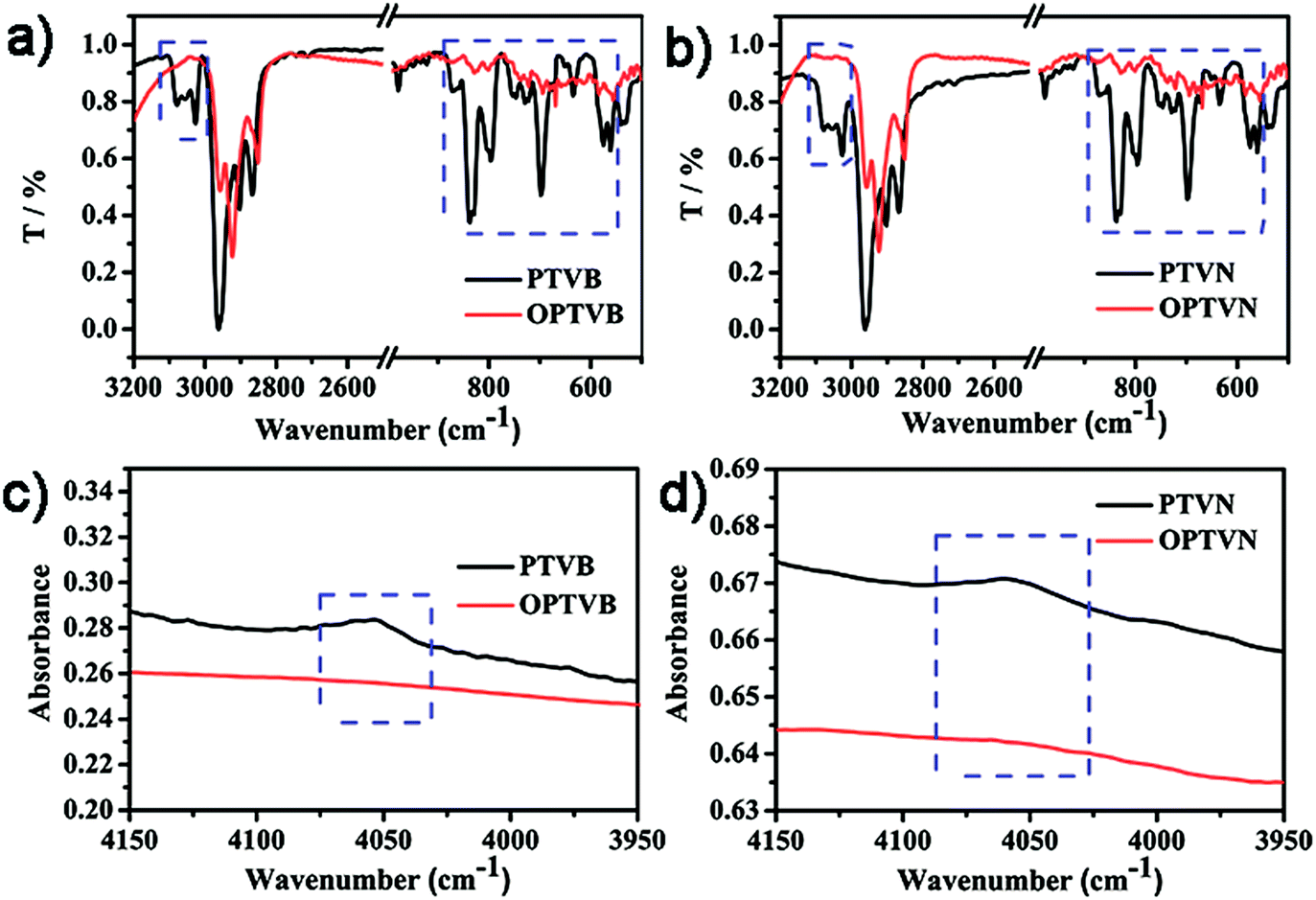 | ||
| Fig. 3 Part of the FTIR spectra within the middle infrared region (500–1000 cm−1, 2500–3200 cm−1) of (a) PTVB and OPTVB, (b) PTVN and OPTVN; part of the FTIR spectra within the near-infrared region (3950–4150 cm−1) of (c) PTVB and OPTVB, (d) PTVN and OPTVN. T denotes transmissivity. | ||
Raman characterization
The results of Raman spectroscopy, which is one of many versatile methods of investigating the structural properties of strap-like polymers, can be found in ESI Fig. S14† to confirm the formation of OPTVB and OPTVN. The spectrum of OPTVB exhibited a first band (D band) located at 1316 cm−1 with a shoulder at 1400 cm−1 and a second band (G band) located at 1575 cm−1. In addition, the D band and G band of OPTVN were located at 1323 cm−1 and 1582 cm−1, respectively. These peaks are consistent with those of similar strap-like polymers synthesized previously by a bottom-up solution-based approach.Thermal properties
The thermal properties of PTVB and PTVN were measured by TGA and DSC in a nitrogen atmosphere (ESI Fig. S15†). The weight loss below 300 °C was ascribed to a small amount of H2O in the macromolecular structure and remaining small molecules. In general, PTVB and PTVN both possessed exceptional thermal stability because of their analogous well-defined structure containing a high proportion of phenyl rings. The decomposition onset temperature of PTVB was 499 °C and that of PTVN was 518 °C, which were assigned to their rigid structures. Moreover, the DSC heating traces of PTVB and PTVN exhibited glass transition temperatures at 214 °C and 234 °C, respectively, in the amorphous region. PTVN possessed better thermal properties because of its greater degree of conjugation and more rigid structure than that of PTVB. The excellent thermal properties of the polymers are favorable for the processing of electronic devices.Self-assembly and morphological characterization
Macromolecules with macroscopic self-assembly behavior always display a number of distinctive and enhanced properties. During the investigation of their morphological characterization, it was interesting to observe the self-assembly behavior of PTVB and PTVN. Fig. 4a and its inset image are POM images of PTVB on different scales. As the POM images show in Fig. 4a and b, many large-area sheet-like microstructures of similar widths were clearly observed using a polarizing microscope. From the pictures, the widths of PTVB and PTVN fibers were estimated to be 1.92 μm and 3.57 μm, respectively. Furthermore, uniform microscale fibrous structures were also identified in SEM images. Fig. 4d shows that PTVN possessed similar, wider fibers than those of PTVB shown in Fig. 4c.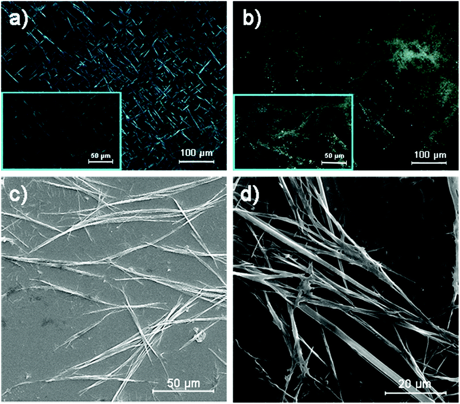 | ||
| Fig. 4 POM images of (a) PTVB and (b) PTVN obtained by slow evaporation of their solutions in THF with a concentration of 1 mg mL−1. The inset images are partial enlarged views. Typical SEM images of (c) PTVB and (d) PTVN obtained by slow evaporation of their solutions in THF with a concentration of 1 mg mL−1. | ||
To further characterize the structures of the strap-like polymers, their XRD patterns were collected, as shown in Fig. 5. The polymer precursors both exhibited a strong diffraction peak at 2θ = 17° corresponding to a calculated d-spacing of 0.521 nm (Fig. 5a and b), which suggests the existence of an orderly structure. Moreover, Fig. 5c and d show the XRD patterns of OPTVB and OPTVN. Obviously, there is a broad, weak characteristic peak at around 2θ = 23° (22.8° for OPTVB and 23.3° for OPTVN), which conforms to the typical characteristic peak of graphite (d002).53,54 Ordinarily, the XRD patterns of an ideal single-layer graphene-like polymer have no characteristic peaks. However, it is impossible to obtain a perfect graphene-like polymer owing to the limits of realistic manufacturing conditions. The appearance of the characteristic peak of graphite indicates that some strap-like polymers were randomly stacked in a disordered graphite structure. Thus, the XRD patterns in this work also confirmed the successful synthesis of nanoribbons with a smaller interplanar spacing of about 0.370 nm because of their greater planarization. Owing to the rough surface of these nanoribbons and the decline in their regularity, the characteristic peak broadened and became attenuated, as shown. However, there was a sharp peak at around 18.4° for PTVB alone. From the above POM images, PTVB exhibited stronger self-assembly behavior in comparison with PTVN. This might result in more pronounced long-range macromolecular order, resulting in the appearance of a sharp peak in the XRD pattern.
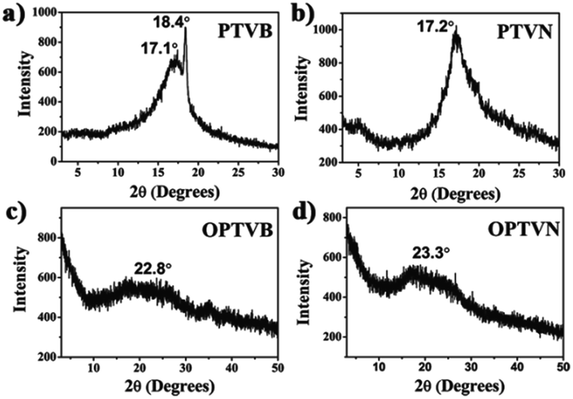 | ||
| Fig. 5 XRD patterns of (a) PTVB, (b) PTVN, (c) OPTVB and (d) OPTVN. | ||
Furthermore, Fig. 6a and b show the corresponding STM images of OPTVB and OPTVN, which provide visual information on their molecular structures. The strap-like molecular structures are clearly observed, as shown in the proposed structural drawings in the magnified images. From these measurements, the widths of the ordered nanoribbons were around 0.29 nm and 0.64 nm, respectively, which were in accordance with the increase in the size of the molecular chains containing naphthalene units. The STM images provide strong confirmation of the successful synthesis of the target conjugated products.
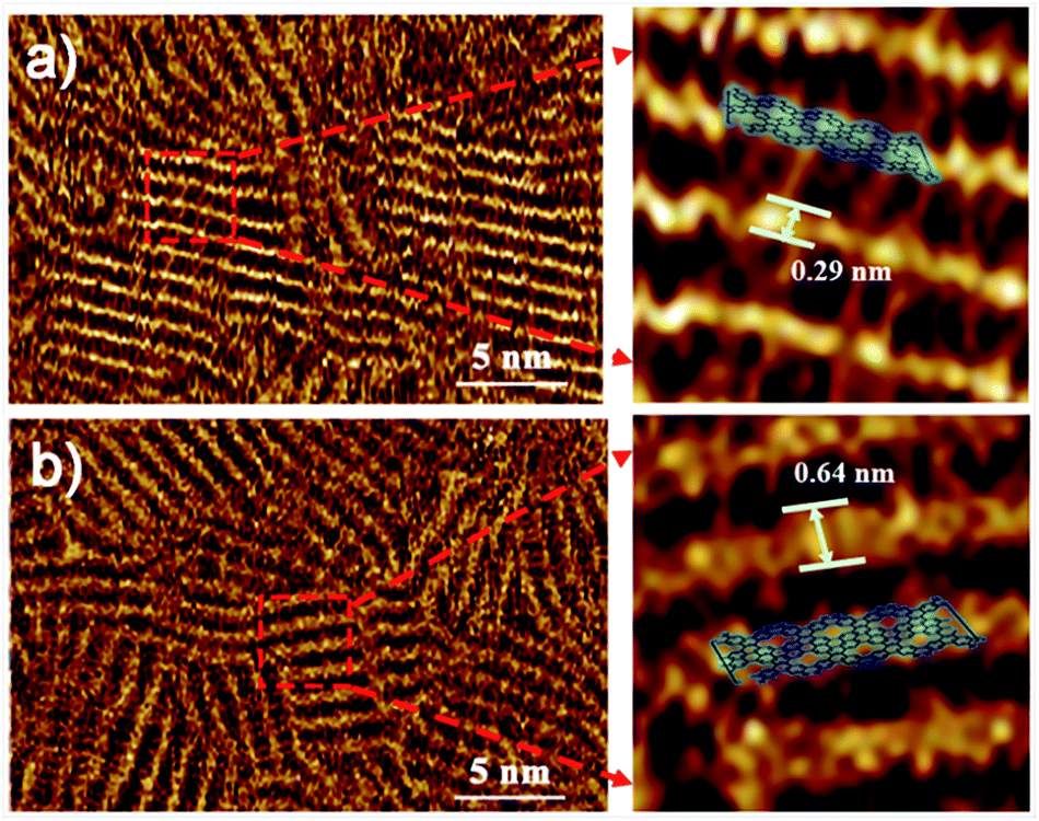 | ||
| Fig. 6 STM images with magnified regions of (a) OPTVB and (b) OPTVN. | ||
Optical properties
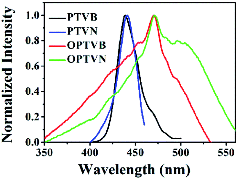
The obtained precursors and nanoribbons could all dissolve in organic solvents such as THF. In comparison to the yellow solutions of PTVB and PTVN in THF, the solutions of OPTVB and OPTVN proved to be light reddish-brown (Fig. 7a). There were some changes in optical properties after cyclodehydrogenation, which could be confirmed clearly by the photoluminescence (PL) spectra in dilute solutions in THF (Fig. 7b). Moreover, the fluorescence photographs obtained under UV exposure shown in Fig. 7c, when roughly observed by the naked eye, could further prove the changes that occurred after locking the phenyl rings of the precursors via chemical cyclization. The measurements were used to investigate how the subtle structural changes modulated the emission colors. Moreover, the detailed excitation spectra of the products are shown in ESI Fig. S8.† In addition, the corresponding spectral data, such as the absorption wavelength (λabs), PL emission wavelength in dilute solution in THF (λem) and in the solid state (λ′em), quantum yield (ΦF) in dilute solution in THF using fluorescein (ΦF = 92% in 0.1 M NaOH solution) as a reference and fluorescence lifetime (τ), are all listed in Table 1. PTVB and PTVN possessed absorption wavelengths of 438 nm and 441 nm, which resulted in red shifts of 32 nm and 30 nm when compared with those of OPTVB and OPTVN, respectively. OPTVB and OPTVN also displayed considerably broader absorptions with some shoulder peaks at 460 nm (OPTVB) and 500 nm (OPTVN). More different excitons formed in the excited states, because electrons can move through the skeleton of polymers with greater π-conjugation. Accordingly, the PL emission peaks of OPTVB and OPTVN in solution in THF, which were located at 542 and 639 nm, displayed a red shift, moving from 485 and 524 nm, respectively. The reason for the bathochromic shift was that the extended conjugation length and planarization of the chains could enhance the extent of the delocalization of π-electrons and narrow the molecular electronic energy level. Thus, this further proved the successful oxidative cyclization between the substituted phenyl rings. Moreover, the Stokes shifts (ΔS) for PTVB, PTVN, OPTVB and OPTVN (53, 72, 83 and 168 nm) confirmed the conformational reorganization in geometry from the pyramidal ground state to a more planar excited state. In addition, the values of ΦF and τ provide convincing evidence for the above conclusions. The ΦF values of PTVB (5.78%) and PTVN (5.79%) were both equally small because of non-radiative deactivation of the excited states caused by the intramolecular rotation of the multiple phenyl rings. The ΦF values of OPTVB and OPTVN increased significantly to 56.58% and 82.95%, respectively, which suggests that ΦF increased with an increase in the degree of conjugation. This coincided well with the different emission colors, as shown in the pictures and PL spectra in solution. From Fig. 7d, it is clear that the τ value of PTVN (1.35 ns) was a little greater than that of PTVB (1.28 ns), which was attributed to the more extended conjugation of the naphthalene ring in PTVN. The τ values of OPTVB and OPTVN rose to 2.92 and 3.14 ns, respectively, which indicates that the luminescence of the excited species in solution could relax much more slowly owing to the restriction of intramolecular rotation, as shown by the changes in ΦF. This was also due to the high rigidity of the chains after intramolecular oxidative cyclization. The photographs in Fig. 7e clearly show their morphology in daylight and fluorescence under UV illumination, together with the PL emission spectra of the solid film (Fig. 7f). By comparison between the photographs in Fig. 7c and the insets in Fig. 7e, PTVB and PTVN both exhibited remarkable aggregation-induced emission (AIE), which is a phenomenon by which some non-luminescent dyes can be induced to emit fluorescent light effectively by the formation of aggregates.55 In the solid film, the molecular chains of the polymers aggregated more closely. Usually, some molecular chains of the polymers are able to pack more closely via π–π stacking owing to their massive phenyl rings and planarization of the nanoribbons, which reduces quenching by the transfer of electrons. Furthermore, the movement of segments in the chains is mostly restricted for reasons of physical constraint. The restriction of intramolecular rotation blocks the non-radiative pathways in solution and opens a radiative channel. In consequence, the emission of light becomes the major mode of the consumption of excitation energy for the polymers in the solid state. In addition, the PL emission peaks of OPTVB and OPTVN, which were located at 627 and 631 nm, both shifted substantially from the yellow spectral region into the red spectral region after cyclization owing to closer packing of the planar chains. The smaller interplanar spacing as a result of stronger π–π stacking enabled electrons to be transferred more easily, which resulted in a more obvious red shift phenomenon. The nanoribbons do not exhibit the AIE phenomenon because of their more rigid structures, which restrain the rotation of the benzene rings (Fig. 8).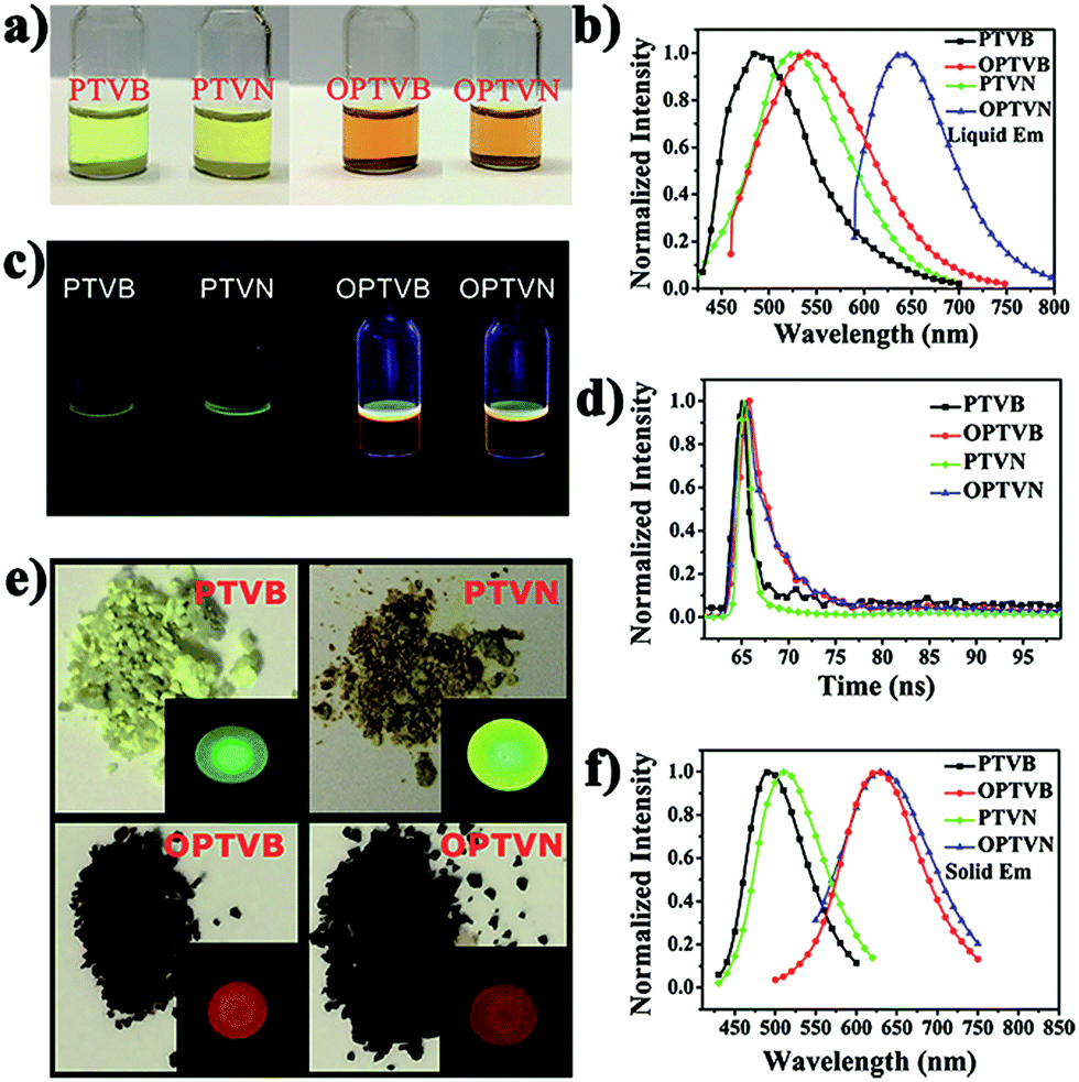 | ||
| Fig. 7 (a) Photographs of solutions of PTVB, PTVN, OPTVB and OPTVN in THF in daylight; (b) normalized PL spectra of PTVB, PTVN, OPTVB and OPTVN in solutions in THF; (c) the corresponding fluorescence photograph of a 1 mg mL−1 solution in THF under 365 nm UV irradiation; (d) fluorescence lifetimes of PTVB, PTVN, OPTVB, and OPTVN in 1 mg mL−1 solutions; (e) photographs of PTVB, PTVN, OPTVB and OPTVN in daylight. The inset pictures are their fluorescence pictures in the solid state under 365 nm UV irradiation; (f) normalized PL spectra of PTVB, PTVN, OPTVB and OPTVN in the solid state. | ||
| λabs (nm) | λem (nm) | ΔS (nm) | λ′em (nm) | ΦF (%) | τ (ns) | Eonset-ox (V) | Eg (eV) | HOMO (eV) | LUMO (eV) | |
|---|---|---|---|---|---|---|---|---|---|---|
| PTVB | 438 | 485 | 53 | 490 | 5.78 | 1.28 | 0.77 | 2.56 | −5.52 | −2.96 |
| OPTVB | 460, 470 | 542 | 72 | 627 | 56.58 | 2.92 | 0.63 | 2.29 | −5.38 | −3.09 |
| PTVN | 441 | 524 | 83 | 530 | 5.79 | 1.35 | 0.82 | 2.37 | −5.57 | −3.20 |
| OPTVN | 471, 500 | 639 | 168 | 649 | 82.95 | 3.14 | 0.73 | 1.94 | −5.48 | −3.55 |
 | ||
| Fig. 8 Normalized excitation spectra of PTVB, PTVN, OPTVB and OPTVN in solution in THF. | ||
Electrochemical properties
In order to better reveal the relationship between the optical properties and electronic structures of the polymers, CV measurements were routinely carried out to determine their electrochemical redox behavior. It is noted that the highest occupied molecular orbital (HOMO), lowest unoccupied molecular orbital (LUMO), and energy band gap (ΔEg) are three essential parameters of electroluminescent materials. The CV curves of the obtained polymers are shown in ESI Fig. S16.† In comparison to the reduction peaks of PTVB and PTVN, the p-undoping (reduction) peaks of OPTVB and OPTVN are inconspicuous in the cyclic voltammograms, which may be due to their better graphene-like structure. The oxidation onset potential (Eonset-ox) determined from CV in acetonitrile could be calculated from these curves. The corresponding data for the polymers, as well as the energy level parameters of the obtained products, are all listed in Table 1. The Eonset-ox values of PTVB, OPTVB, PTVN and OPTVN versus an Ag electrode appeared at 0.77, 0.63, 0.82 and 0.73 V, respectively. On the basis of the Eonset-ox values and the oxidation process, the HOMO energy levels of the polymers were estimated to be −5.52, −5.38, −5.57 and −5.48 eV, respectively. The ΔEg values were therefore calculated to be 2.56, 2.29, 2.37 and 1.94 eV, respectively, which were determined by the onset wavelength of the UV absorption spectra. The decrease in the band gaps indicates that the strap-like polymers possess good conducting properties owing to their greater conjugation length and planarization.Using the Gaussian 09 program,56 we performed DFT calculations on OPTVB-1 and OPTVB-2 to provide evidence of the complete cyclodehydrogenation. Model molecules with four repeating units of OPTVB-1 and OPTVB-2 (one containing defects) were selected as examples because of the simple calculations involved (Fig. S17†). The calculated band gaps of OPTVB-1 and OPTVB-2 are 2.749 eV and 2.837 eV, respectively. Defects can contribute to an increase in band gaps, which is illustrated by the greater distortion of planarity in OPTVB-2. The experimental band gap (2.79 eV) of the OPTVB polymer is in accordance with the result (2.749 eV) calculated for OPTVB-1. This basically shows that the obtained GNRs might have been fully oxidized by FeCl3 in sufficient time.
FETs characterization
After the above characterizations, OPTVB and OPTVN displayed potential to be employed in devices such as FETs. Here, the obtained nanoribbons were utilized as the semiconductor layer in FETs to measure their anticipated electron transmission capacity. Unlike common FETs, in which the gate dielectric is a typical inorganic oxide such as Al2O3, SiO2 and ZrO2, one fascinating feature is the utilization of an ion gel as the gate dielectric.57,58 Notwithstanding the fact that several high-performance FETs with inorganic dielectrics have been manufactured by some research groups,59,60 organic dielectrics such as ion gels exhibit unique advantages. Not only do they have remarkable mechanical flexibility like most organic materials, their extraordinarily high capacitance also permits low-voltage operation. This is an effective way to take advantage of a low working voltage to decrease the quantity of heat generated by the working device. Therefore, an ion gel was selected for combination with the obtained nanoribbons as a semiconductor for fabricating FETs.Fig. 9a shows a simple 3D model displaying the geometric structure of a thin-film top-gate FET with aluminum as the top gate and an ion gel coated on gold electrodes as the dielectric layer. Fig. 9b is a photograph of practical FET devices that we prepared. The detailed manufacturing process of the FET devices can be found in the ESI.† As depicted in Fig. 9c and d, the output curves confirmed clearly that the FETs displayed p-channel FET characteristics with the strap-like polymers in the devices. Moreover, the original transfer characteristic curves and gate leakage curves of OPTVB and OPTVN (ESI Fig. S18 and S19†) show that a low gate leakage current has no notable impact on the drain current. From the linear relationship within a limited range between ∣IDS∣1/2 and ∣VG∣ in the curve obtained at VDS = 3.5 V, as shown in Fig. 9e and f, the threshold voltages (Vth) of the FETs with OPTVB and OPTVN were determined to be −0.28 V and −0.54 V, respectively.
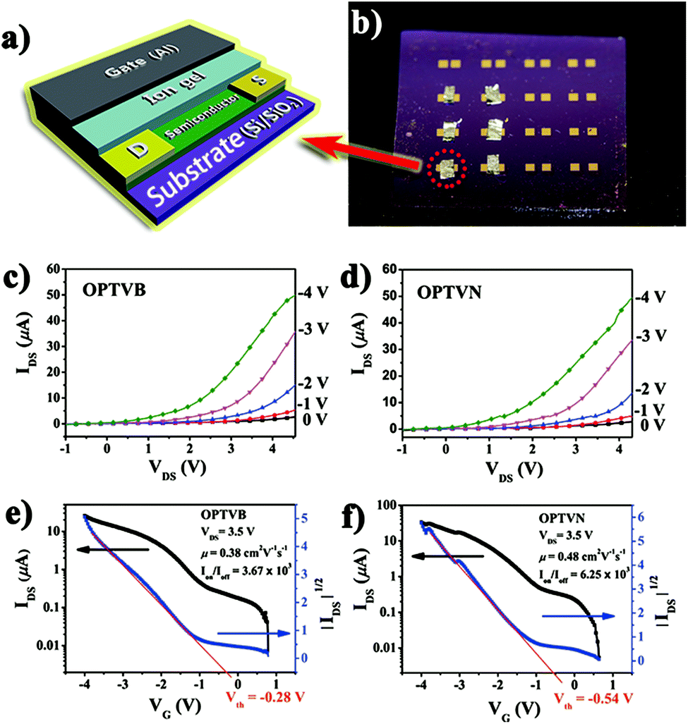 | ||
| Fig. 9 (a) 3D model showing the geometric structure of the fabricated top-gate FET; (b) photograph of the practical FETs; output characteristics of FETs consisting of (c) OPTVB and (d) OPTVN; transfer characteristic curve at a drain–source voltage (VDS) of 3.5 V of FETs consisting of (e) OPTVB and (f) OPTVN. | ||
The gate oxide capacitance per unit area of the ion gel prepared in this work was measured to be 20 μF cm−2. The transfer characteristics included low conductivity at a low VG value of around 0 V, which indicated promising stability in air owing to the low HOMO energy levels (−5.38 eV and −5.48 eV) of OPTVB and OPTVN. According to the Vth values and the transfer characteristics, some groups of IDS and VG values were substituted into the above formula to obtain several μ values. The detailed calculations are displayed in the ESI.† An illustration of plots of calculated mobility versus the related gate voltage for OPTVB and OPTVN is also shown in ESI Fig. S20.† In comparison with some FETs with high mobility but low Ion/Ioff values, our fabricated FETs could function at a lower voltage (<5 V). In general, high mobility with a good Ion/Ioff value is selected for optimal performance in preference to only one good parameter. The optimal μ value of OPTVB was 0.38 cm2 V−1 s−1 with an Ion/Ioff value of 3.67 × 10³, and the optimal μ value of OPTVN was 0.48 cm2 V−1 s−1 with an Ion/Ioff value of 6.25 × 10³. The good μ and Ion/Ioff values of the FETs containing OPTVB and OPTVN tallied with their good conducting properties, as was expected. The lower operating voltage was also another major advantage in the field of practical application of the organic FETs.
Conclusions
In summary, in order to obtain well-defined strap-like conjugated polymers based on TPE by straightforward bottom-up solution processing, two novel alternating polymer precursors, namely, PTVB and PTVN, with high molecular weights were successfully designed and synthesized via Suzuki cross-coupling polymerization in good yields. Furthermore, PTVB and PTVN both exhibited unexpected self-assembly, as shown in our micrographic observations of their morphology. Then, anhydrous FeCl3 was used in an oxidative cyclodehydrogenation reaction to convert PTVB and PTVN into OPTVB and OPTVN, respectively. The formation of conjugated strap-like polymers was clearly characterized by a number of techniques such as NMR, XRD, STM, UV/vis absorption, PL, Raman and FTIR spectra.The preliminary photoluminescence spectra, which exhibited a red shift, and the corresponding changes in band gaps measured by electrochemical analysis both proved the increased electron transmission capacity of the synthesized strap-like polymers with extended planarization. In comparison, OPTVN possessed a greater degree of conjugation and greater width of ribbons because of the introduction of naphthalene rings and displayed better planarization and electron transmission, as was anticipated. In addition, the high thermal stability of the polymers provided more advantages for patterning integrated nano- or micro-optoelectronic devices. For this reason, a batch of outstanding top-gated FETs were successfully developed with OPTVB and OPTVN films as the active semiconductor layer in combination with ion gel dielectrics. The fabricated devices not only had excellent stability in air, but also displayed high performance at low working voltages, which suggested extensive potential for fabricating practical, mechanically flexible and high-performance electronic devices.
Acknowledgements
This work was financially supported by the National Natural Science Foundation of China (21274027 and 20974022) and the Innovation Program of Shanghai Municipal Education Commission (15ZZ002). The computation work was supported by the A*STAR Computational Resource Centre through the use of its high-performance computing facilities. The FET devices were fabricated and probed in the nanofab of Fudan University.Notes and references
- K. S. Novoselov, A. K. Geim, S. V. Morozov, D. Jiang, Y. Zhang, S. V. Dubonos, I. V. Grigorieva and A. A. Firsov, Science, 2004, 306, 666–669 CrossRef CAS PubMed.
- H. Cong, J. Chen and S. Yu, Chem. Soc. Rev., 2014, 43, 7295–7325 RSC.
- K. Müllen, ACS Nano, 2014, 8, 6531–6541 CrossRef PubMed.
- X. Zhou, L. Wan and Y. Guo, Chem. Commun., 2013, 49, 1838 RSC.
- N. Liu, H. Tian, G. Schwartz, J. B. H. Tok, T. Ren and Z. Bao, Nano Lett., 2014, 14, 3702–3708 CrossRef CAS PubMed.
- T. Cui, R. Lv, Z. Huang, S. Chen, Z. Zhang, X. Gan, Y. Jia, X. Li, K. Wang, D. Wu and F. Kang, J. Mater. Chem. A, 2013, 1, 5736 CAS.
- Y. Xue, B. Wu, Q. Bao and Y. Liu, Small, 2014, 10, 2975–2991 CrossRef CAS PubMed.
- E. Shi, H. Li, L. Yang, L. Zhang, Z. Li, P. Li, Y. Shang, S. Wu, X. Li, J. Wei, K. Wang, H. Zhu, D. Wu, Y. Fang and A. Cao, Nano Lett., 2013, 13, 1776–1787 CrossRef CAS PubMed.
- L. Wang, B. Wu, J. Chen, H. Liu, P. Hu and Y. Liu, Adv. Mater., 2014, 26, 1559–1564 CrossRef CAS PubMed.
- J. Tang, G. Chen, J. Yang, X. Zhou, L. Zhou and B. Huang, Nano Energy, 2014, 8, 62–70 CrossRef CAS.
- Z. Du, W. Ai, L. Xie and W. Huang, J. Mater. Chem. A, 2014, 2, 9164 CAS.
- J. Wu, W. Pisula and K. Müllen, Chem. Rev., 2007, 107, 718–747 CrossRef CAS PubMed.
- A. H. C. Neto, F. Guinea, N. M. R. Peres, K. S. Novoselov and A. K. Geim, Rev. Mod. Phys., 2009, 81, 109–162 CrossRef.
- K. Zou, F. Zhang, C. Clapp, A. H. MacDonald and J. Zhu, Nano Lett., 2013, 13, 369–373 CrossRef CAS PubMed.
- L. Britnell, R. V. Gorbachev, R. Jalil, B. D. Belle, F. Schedin, A. Mishchenko, T. Georgiou, M. I. Katsnelson, L. Eaves, S. V. Morozov, N. M. R. Peres, J. Leist, A. K. Geim, K. S. Novoselov and L. A. Ponomarenko, Science, 2012, 335, 947–950 CrossRef CAS PubMed.
- H. Xu, Z. Zhang, Z. Wang, S. Wang, X. Liang and L. Peng, ACS Nano, 2011, 5, 2340–2347 CrossRef CAS PubMed.
- K. Thiyagarajan, B. Saravanakumar, R. Mohan and S. Kim, ACS Appl. Mater. Interfaces, 2013, 5, 6443–6446 CAS.
- A. J. Samuels and J. D. Carey, ACS Nano, 2013, 7, 2790–2799 CrossRef CAS PubMed.
- G. S. Kliros, Nanoscale Res. Lett., 2014, 9, 65 CrossRef PubMed.
- R. Balog, B. Jørgensen, L. Nilsson, M. Andersen, E. Rienks, M. Bianchi, M. Fanetti, E. Lægsgaard, A. Baraldi, S. Lizzit, Z. Sljivancanin, F. Besenbacher, B. Hammer, T. G. Pedersen, P. Hofmann and L. Hornekær, Nat. Mater., 2010, 9, 315–319 CrossRef CAS PubMed.
- B. R. Matis, J. S. Burgess, F. A. Bulat, A. L. Friedman, B. H. Houston and J. W. Baldwin, ACS Nano, 2012, 6, 17–22 CrossRef CAS PubMed.
- M. Y. Han, B. Özyilmaz, Y. Zhang and P. Kim, Phys. Rev. Lett., 2007, 98, 206805 CrossRef PubMed.
- M. Koch, F. Ample, C. Joachim and L. Grill, Nat. Nanotechnol., 2012, 7, 713–717 CrossRef CAS PubMed.
- W. Y. Kim and K. S. Kim, Nat. Nanotechnol., 2008, 3, 408–412 CrossRef CAS PubMed.
- P. Zhao, J. Chauhan and J. Guo, Nano Lett., 2009, 9, 684–688 CrossRef CAS PubMed.
- L. Ma, J. Wang and F. Ding, Angew. Chem., Int. Ed., 2012, 51, 1161–1164 CrossRef CAS PubMed.
- S. S. Datta, D. R. Strachan, S. M. Khamis and A. T. C. Johnson, Nano Lett., 2008, 8, 1912–1915 CrossRef CAS PubMed.
- G. Liu, Y. Wu, Y. Lin, D. B. Farmer, J. A. Ott, J. Bruley, A. Grill, P. Avouris, D. Pfeiffer, A. A. Balandin and C. Dimitrakopoulos, ACS Nano, 2012, 6, 6786–6792 CrossRef CAS PubMed.
- W. Yoon, Y. Lee, H. Jang, M. Jang, J. S. Kim, H. S. Lee, S. Im, D. W. Boo, J. Park and S. Ju, Carbon, 2015, 81, 629–638 CrossRef CAS.
- Q. Peng, Y. Li, X. He, X. Gui, Y. Shang, C. Wang, C. Wang, W. Zhao, S. Du, E. Shi, P. Li, D. Wu and A. Cao, Adv. Mater., 2014, 26, 3241–3247 CrossRef CAS PubMed.
- J. Sun, T. Iwasaki, M. Muruganathan and H. Mizuta, Appl. Phys. Lett., 2015, 106, 033509 CrossRef.
- W. S. Hwang, P. Zhao, K. Tahy, L. O. Nyakiti, V. D. Wheeler, R. L. Myers-Ward Jr, C. R. Eddy, D. K. Gaskill, J. A. Robinson, W. Haensch, H. G. Xing, A. Seabaugh and D. Jena, APL Mater., 2015, 3, 011101 CrossRef.
- S. Aigner, L. D. Pietra, Y. Japha, O. Entin-Wohlman, T. David, R. Salem, R. Folman and J. Schmiedmayer, Science, 2008, 319, 1226–1229 CrossRef CAS PubMed.
- L. Jiao, X. Wang, G. Diankov, H. Wang and H. Dai, Nat. Nanotechnol., 2010, 5, 321–325 CrossRef CAS PubMed.
- Z. B. Shifrina, M. S. Averina, A. L. Rusanov, M. Wagner and K. Müllen, Macromolecules, 2000, 33, 3525–3529 CrossRef CAS.
- N. Liu, K. Kim, P. Hsu, A. N. Sokolov, F. L. Yap, H. Yuan, Y. Xie, H. Yan, Y. Cui, H. Y. Hwang and Z. Bao, J. Am. Chem. Soc., 2014, 136, 17284–17291 CrossRef CAS PubMed.
- A. Chuvilin, E. Bichoutskaia, M. C. Gimenez-Lopez, T. W. Chamberlain, G. A. Rance, N. Kuganathan, J. Biskupek, U. Kaiser and A. N. Khlobystov, Nat. Mater., 2011, 10, 687–692 CrossRef CAS PubMed.
- J. Cai, C. A. Pignedoli, L. Talirz, P. Ruffieux, H. Söde, L. Liang, V. Meunier, R. Berger, R. Li, X. Feng, K. Müllen and R. Fasel, Nat. Nanotechnol., 2014, 9, 896–900 CrossRef CAS PubMed.
- J. Wu, L. Gherghel, M. D. Watson, J. Li, Z. Wang, C. D. Simpson, U. Kolb and K. Müllen, Macromolecules, 2003, 36, 7082–7089 CrossRef CAS.
- X. Yang, X. Dou, A. Rouhanipour, L. Zhi, H. J. Räder and K. Müllen, J. Am. Chem. Soc., 2008, 130, 4216–4217 CrossRef CAS PubMed.
- K. T. Kim, J. W. Jung and W. H. Jo, Carbon, 2013, 63, 202–209 CrossRef CAS.
- W. Wang, T. Lin, M. Wang, T. Liu, L. Ren, D. Chen and S. Huang, J. Phys. Chem. B, 2010, 114, 5983–5988 CrossRef CAS PubMed.
- Z. Zhao, J. W. Y. Lam and B. Z. Tang, J. Mater. Chem., 2012, 22, 23726–32374 RSC.
- J. Ma, T. Lin, X. Pan and W. Wang, Chem. Mater., 2014, 26, 4221–4229 CrossRef CAS.
- H. Wang, T. Lin, J. Ma and W. Wang, Tetrahedron, 2014, 70, 5046–5051 CrossRef CAS.
- A. Narita, X. Feng and K. Müllen, Chem. Rec., 2015, 15, 295–309 CrossRef CAS PubMed.
- N. Miyaura and A. Suzuki, Chem. Rev., 1995, 95, 2457–2483 CrossRef CAS.
- R. Wu, S. Hu, H. Xu, X. Wei and L. Hu, J. Photochem. Photobiol., B, 2007, 88, 180–184 CrossRef CAS PubMed.
- C. D. Simpson, G. Mattersteig, K. Martin, L. Gherghel, R. E. Bauer, H. J. Räder and K. Müllen, J. Am. Chem. Soc., 2004, 126, 3139–3147 CrossRef CAS PubMed.
- A. Pradhan, P. Dechambenoit, H. Bock and F. Durola, Angew. Chem., Int. Ed., 2011, 50, 12582–12585 CrossRef CAS PubMed.
- A. Narita, I. A. Verzhbitskiy, W. Frederickx, K. S. Mali, S. A. Jensen, M. R. Hansen, M. Bonn, S. De Feyter, C. Casiraghi, X. Feng and K. Müllen, ACS Nano, 2014, 8, 11622–11630 CrossRef CAS PubMed.
- L. Dössel, L. Gherghel, X. Feng and K. Müllen, Angew. Chem., Int. Ed., 2011, 50, 2540–2543 CrossRef PubMed.
- O. C. Compton, B. Jain, D. A. Dikin, A. Abouimrane, K. Amine and S. T. Nguyen, ACS Nano, 2011, 5, 4380–4391 CrossRef CAS PubMed.
- J. Lin, Z. Peng, C. Xiang, G. Ruan, Z. Yan, D. Natelson and J. M. Tour, ACS Nano, 2013, 7, 6001–6006 CrossRef CAS PubMed.
- Y. Hong, J. W. Y. Lam and B. Z. Tang, Chem. Soc. Rev., 2011, 40, 5361–5388 RSC.
- M. J. Frisch, G. W. Trucks and H. B. Schlegel, et al., Gaussian 09 Revision A.2, Gaussian, Inc., Wallingford CT, 2009 Search PubMed.
- C. Zhang, Y. Zang, E. Gann, C. R. McNeill, X. Zhu, C. Di and D. Zhu, J. Am. Chem. Soc., 2014, 136, 16176–16184 CrossRef CAS PubMed.
- J. Huang, J. Pu, C. Hsu, M. Chiu, Z. Juang, Y. Chang, W. Chang, Y. Iwasa, T. Takenobu and L. Li, ACS Nano, 2014, 8, 923–930 CrossRef CAS PubMed.
- Y. Yuan, G. Giri, A. L. Ayzner, A. P. Zoombelt, S. C. B. Mannsfeld, J. Chen, D. Nordlund, M. F. Toney, J. Huang and Z. Bao, Nat. Commun., 2014, 5, 3005 Search PubMed.
- Y. Zhou, T. Lei, L. Wang, J. Pei, Y. Cao and J. Wang, Adv. Mater., 2010, 22, 1484–1487 CrossRef CAS PubMed.
Footnote |
| † Electronic supplementary information (ESI) available: MALDI-TOF, 1H NMR and 13C NMR spectra of all the synthesized products, absorption spectra and cyclic voltammetry of PTVB, PTVN, OPTVB and OPTVN, Raman spectra of OPTVB and OPTVN, DSC and TGA spectra of PTVB and PTVN, calculated HOMO and LUMO energy levels of OPTVB, calculated procedures for the charge carrier mobility of the fabricated FETs. CCDC 1425688 and 1425689, crystal structure data for 1 and 2. For ESI and crystallographic data in CIF or other electronic format see DOI: 10.1039/c6ra25214a |
| This journal is © The Royal Society of Chemistry 2017 |