
 Open Access Article
 This Open Access Article is licensed under a
 Creative Commons Attribution 3.0 Unported Licence
Improved electron extraction by a ZnO nanoparticle interlayer for solution-processed polymer solar cells†
Xuning Zhangab,
Shuo Yangb,
Shiqing Bib,
Anbu Kumaresanb,
Jiyu Zhouc,
Jason Seifterd,
Hongyu Mia,
Yun Xue,
Yuan Zhang*c and
Huiqiong Zhou *b
*b
aXinjing Uygur Autonomous Region Key Laboratory of Coal Clean Conversion and Chemical Engineering Process, School of Chemistry and Chemical Engineering, Xinjiang University, Urumqi 830046, P. R. China
bCAS Key Laboratory of Nanosystem and Hierarchical Fabrication, CAS Center for Excellence in Nanoscience, National Center for Nanoscience and Technology, Beijing 100190, China. E-mail: zhouhq@nanoctr.cn
cHEEGER Beijing Research & Development Center, School of Chemistry and Environment, Beihang University, Beijing 100191, P. R. China. E-mail: yuanzhang@buaa.edu.cn
dCenter for Polymers and Organic Solids, University of California at Santa Barbara, Santa Barbara, California 93106, USA
eCenter for Medical Device Evaluation, China Food and Drug Administration, Beijing, 100044, China
First published on 21st February 2017
Abstract
Charge injection/extraction properties dictate the device characteristics of polymer solar cells. Based on a model system comprising PTB7-Th:PC71BM blends, we investigate solvent effects and interface properties of ZnO nanoparticles used as electron-transporting/hole blocking interlayers (ETL/HBL) to improve the solar cell performance and stability. We find that the polarity of processing solvents and thickness of ZnO nanoparticles ETL both play a crucial role in the device behavior. Under the optimal conditions, the power conversion efficiency (PCE) is increased from 8.4% to 9.2% for PTB7-Th:PC71BM solar cells with a conventional device architecture, which is among the highest efficiencies for this blend system. The simultaneous increase in short-circuit current (Jsc) and fill factor (FF) originates from an effective hole blocking mechanism provided by the ZnO layers which increase the selectivity of charge extraction and reduce non-geminate charge recombination. The dense and air-stable ZnO ETLs minimize the diffusion of moisture and O2 into the photoactive layer, leading to drastically improved device stability.
1. Introduction
Polymer solar cells (PSCs) based on polymer–fullerene bulk heterojunctions (BHJ) offer great potential for renewable energy because of their low-cost, light-weight, flexibility, and ability to manufacture using roll-to-roll printing technology.1 Currently the application of PCSs is mainly limited by their relatively low power conversion efficiency (PCE) and unsatisfactory stability. To conquer these limitations, research has been centred on new materials design, morphological optimization of the BHJ active layer or interface, and device architecture engineering. A widely adopted design rule for donor materials is to reduce their band-gaps to increase the photon harvesting and resultant short-circuit current (Jsc). Through maintaining a deep highest occupied molecular orbital (HOMO) in the donor, a large energetic offset between the lowest unoccupied molecular orbital (LUMO) of the acceptor and the HOMO of polymer donor is attained which enables a high open-circuit voltage (Voc).2–4 Recently emerging non-fullerene acceptors have become alternatives to PCBM, offering competitive PCEs over 12% when used in polymer solar cells.5–7 Generally speaking the morphology of donor and acceptor molecules plays important roles in the charge generation, dissociation and transport processes in BHJ devices. These processes are controllable to certain degree through optimizing the donor/acceptor compositional ratio or the phase separation with processing based on solvent additives,8 thermal or solvent annealing etc.9,10 In addition to the photoactive layer, interfaces within the solar cell device architecture are also important for device operation because dissociated carriers must be extracted eventually at the contacts to render the photovoltaic effect. If the density of carriers is non-uniformly distributed throughout the active layer, typically higher in regions near the contact with the presence of charge extraction barriers, reduction of the built-in potential occurs, resulting in an acceleration of charge recombination such that PCEs are decreased. To circumvent these effects, interface thin films (electron transporting layer, ETL, or hole transporting layer, HTL) have been inserted between the BHJ layer and the electrodes, leading to noticeable enhancements of charge collection efficiency and ultimate PCEs.11–21Among utilized interface materials, transparent metal oxides (TCO) and organic molecules have shown success in mediating charge extraction and selective charge blocking properties. For TCOs, high temperature thermal annealing is often required to achieve the necessary electrical conductivity, which to certain degree complicates the processing and device fabrication. Organic molecules mainly resort to dipole interaction to render the interface effect and typically do not require high temperature processing. However due to their low electrical conductivity, the film thickness needs to be very low, normally in a few nanometres. This inevitably raises an issue of reproducibility and robustness.
ZnO thin films with a high stability, satisfactory optical transparency and fit work function (WF) are excellent candidate materials for ETLs in organic solar cells with inverted device structure.16,22–28 The needed high temperature annealing, consistent with the general requirement of TCO processing not only is time- and energy consuming but also imposes a difficulty for use with conventional device structure concerning the temperature-sensitivity of BHJ layer. These disadvantages are bypassed by the formation of ZnO nanoparticles using low temperature processing which provide great flexibility for different device architectures.24 Despite of these merits, this approach is sensitive to the processing conditions. Therefore optimizing the processing of ZnO nanoparticles HBL and understanding the factors that influence the properties are of great importance to further advance the interface engineering and device performance in polymer solar cells. To the best of our knowledge, these aspects are not fully clarified yet, thus are worthy of further investigation.
In this work, we synthesize ZnO nanoparticles which are incorporated as an ETL/HBL into polymer solar cells comprising of poly{2-ethylhexyl 6-(4,8-bis(5-(2-ethylhexyl)thiophen-2-yl)-6-methylbenzo[1,2-b:4,5-b′]dithiophen-2-yl)-3-fluoro-4-methylthieno[3,4-b]thiophene-2-carboxylate} (PTB7-Th, molecular structure shown in Fig. 1a, inset) donor in blend with [6,6]-phenyl C71-butyric acid methyl ester (PC71BM) acceptor. We investigate the influences of processing for ZnO nanoparticle ETLs, and resultant device behaviour and stability. Because of the energies of the ionization potential and electron affinity of ZnO, a high transparency in the visible range is attained which minimizes light losses in devices. Compared to the sol–gel method, ZnO nanoparticles do not require high temperature thermal annealing in order to render desired electrical functionalities, thus providing an easy and reproducible route. We found that the polarity of the processing solvents and thickness of ZnO nanoparticles thin films play a crucial role in the device behavior. In the optimal condition, the power conversion efficiency (PCE) is increased from 8.4% to 9.2% for PTB7-Th:PC71BM solar cells. The excellent hole blocking property of ZnO ETLs, confirmed by charge injection measurements, increases the selectivity of charge extraction at the cathode, leading to increased Jsc and fill factor (FF). In addition, the ZnO ETLs are dense and air-stable which therefore act as an effective protection for BHJ layers from H2O and O2. As a result, the PCE and stability of PTB7-Th:PC71BM solar cells are simultaneously improved after incorporating ZnO ETLs. In comparison to the results of ZnO ETLs used in inverted solar cells, we achieve similar enhancements in the PCE with conventional structure. The enhancement mainly benefits from the optimized opto-electrical properties in ZnO ETLs, desired morphology in the active layer and the exclusive charge extraction at the cathode interface.2,22,23
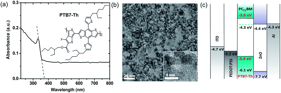 | ||
| Fig. 1 (a) Absorption spectrum of ZnO nanoparticle thin film on quartz. Inset: molecular structure of PTB7-Th. (b) Bright-field TEM image of ZnO nanoparticles. Inset: HR-TEM image. (c) Energetic diagram of the components in PTB7-Th:PC71BM solar cells. | ||
2. Experimental
2.1 Synthesis of ZnO nanoparticles
General procedure used for the preparation of ZnO nanoparticles is as follows: zinc acetate dihydrate (2.95 g) was dissolved and stirred in methanol (125 mL) at 60 °C for 30 min. A solution of potassium hydroxide in methanol (1.48 g/65 mL) was added into the zinc acetate dihydrate solution. Then the reaction mixture was stirred at 60 °C for 2 h. The resulting solution was washed and transferred into a plastic tube and then centrifuged at 3000 rpm for 5 min to separate the precipitate and mother liquor. Then, ZnO precipitates were dissolved in 2-methoxyethanol (2ME), isopropanol (IPA), and the mixed solvent of 2ME![[thin space (1/6-em)]](https://www.rsc.org/images/entities/char_2009.gif) :IPA = 1:1 with different concentrations for different thicknesses.
:IPA = 1:1 with different concentrations for different thicknesses.
2.2 Device fabrication
PTB7-Th (named as PCE10) was purchased from 1-Material Chemscitech Inc. (St-Laurent, Quebec, Canada) and used as received. The device structure was ITO/PEDOT:PSS/PTB7-Th:PC71BM/Al. A thin layer (∼30 nm) of PEDOT:PSS (Baytron PVP Al 4083) was spin-coated onto a cleaned ITO surface and annealed in air at 140 °C for 10 min. Then, active layers of PTB7-Th:PC71BM were cast from the solution with a PTB7-Th:PC71BM ratio of 1:1.5 (PTB7-Th concentration of 10 mg mL−1 in chlorobenzene/1,8-diiodoctane (97:3 vol%) mixture solvent) at a spin-rate of 2000 rpm for 2 min. ZnO nanoparticles in different solutions were cast on top of PTB7-Th:PC71BM layers at a spin-rate of 3000 rpm for 40 s. The devices were completed after deposition of 100 nm Al as cathode (4.5 mm2). Devices were encapsulated for testing in air with a UV-curable epoxy and covered with a glass slide.
2.3 Characterization
Current density–voltage (J–V) characteristics of solar cells were measured by a Keithley 2400 Source Measure Unit, and a Newport Air Mass 1.5 Global (AM 1.5 G) full spectrum solar simulator with an irradiation intensity of 100 mW cm−2. In all cases a circular aperture (3.98 mm2) was used for obtaining the current–voltage curves. The 100 mW cm−2 spectrum of incident light was spectrum and intensity matched with an Ocean Optics USB4000 spectrometer calibration standard lamp with NIST-traceable calibration from 350–1000 nm. External quantum efficiency (EQE) spectra were measured using a 75 W Xe lamp, Newport monochrometer, Newport optical chopper, and a Stanford Research Systems lock-in amplifier. Power-density calibration was done with a National Institute of Standards and Technology traceable silicon photodiode.For illumination intensity dependence J–V measurement, the intensity of the light was modulated with a series of two neutral density filters wheels of six filters apiece. The intensity of light transmitted through the filter was independently measured via a power meter. SCLC measurements for PTB7-Th:PC71BM devices were explored in configuration of ITO/PEDOT:PSS/active layer/MoOx/Au for hole-only devices.
The device absorption was measured by UV-vis-NIR spectrophotometer system (PerkinElmer Lambda 950) in reflection-mode measurement inside of an integrating sphere. AFM images were captured with Asylum MFP3D. The thicknesses of the individual layers in the cells were determined by a surface profiler and verified with AFM. TEM analysis (FEI Tecnai T20, operated at 200 kV) included bright-field and HR imaging.
3. Results and discussion
3.1 Device optimization
ZnO nanoparticles used in this work were synthesized by a solution method.29,30 The absorption spectrum of ZnO thin film (Fig. 1a) shows a steep absorbance peak with a cut off at 374 nm, implying that the band-gap of ZnO nanoparticle film is 3.3 eV. The high transparency of ZnO nanoparticle thin films in the spectral range from 400 nm to 800 nm minimizes the absorption loss when incorporated in solar cells as ETLs. Fig. 1b shows the transmission electron microscopic (TEM) image of the ZnO nanoparticles. A homogeneous size distribution is observed with an average particle diameter of 5 nm. As shown in the inset, the lattice fringes are clearly observed in the high-resolution TEM image, indicative of a high crystallinity for the ZnO nanoparticles.The device structure of the PTB7-Th:PC71BM BHJ solar cells with the ZnO nanoparticle ETL is shown schematically in Fig. 1c. The ZnO nanoparticle interlayer was inserted between the PTB7-Th:PC71BM active layer and the Al cathode. According to the energy diagrams in Fig. 1d, the ZnO nanoparticles have an electron affinity of 4.4 eV and an ionization potential of 7.7 eV.24 Thus, the electronic structure of ZnO nanoparticles provides an efficient electron extraction from PTB7-Th:PC71BM toward the Al cathode, and also blocks the holes at the BHJ/ZnO interface because of the energetic offset between the HOMO of PTB7-Th and the ionization potential of ZnO nanoparticles. Due to the absence of organic ligands on the ZnO nanoparticles, surface trapping effect for charge carriers is minimized which is an important issue in nanomaterial devices.
Current density–voltage (J–V) characteristics under AM 1.5 G irradiation (100 mW cm−2) of PTB7-Th:PC71BM solar cells with ZnO thin films with different thicknesses fabricated from different solvents are shown in Fig. 2a. Detailed device parameters are summarized in Table 1. Processing with three solvents, 2-methoxyethanol (2ME), isopropanol (IPA), and the mixed solvent of 2ME:IPA = 1:1, for ZnO nanoparticle solution has been studied. Based on our experience, the dissolubility of ZnO nanoparticles is better in 2ME than in IPA, while the film quality of ZnO deposited on top of BHJ layers from IPA is more superior to the one from 2ME. Thus, the mixed solvent 2ME:IPA is expected to balance these features. The maximum thickness of ZnO thin films from 2ME, 2ME:IPA, IPA are 50 nm, 30 nm, 15 nm respectively as measured by profilometry. Fig. S1† shows surface topographic images captured by atomic force microscopy (AFM) of ZnO thin films coated on PTB7-Th:PC71BM with different thicknesses processed from different solvents. We observe a reduced surface roughness (RMS) when the thickness of ZnO decreases or the ratio of IPA increases. Devices with ZnO processed from 2ME exhibit slightly reduced Jsc compared to that with 2ME:IPA or pure IPA solvents. As seen from Table 1, the FF and Voc seem less sensitive to the choice of solvents, showing consistent values. From the 2ME solvent, the device with 30 nm ZnO ETLs shows the best PCE = 8.8% with a Jsc = 15.65 mA cm−2, Voc = 0.78 V, and FF = 72.1%. Generally, a thicker ZnO (50 nm) film produces a smaller Jsc, mainly due to the higher resistance while the device with thinner film (15 nm) suffers from a worse FF. The optimal process for ZnO HBLs is found to be around 30 nm from 2ME:IPA solvent, leading to an increased PCE = 9.2%, which may originate from the balance between ZnO thickness and film quality.
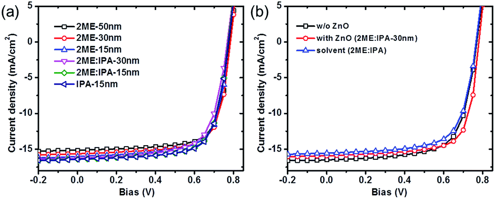 | ||
| Fig. 2 Current-density (J–V) characteristics of PTB7-Th:PC71BM solar cells under irradiation: (a) with various thicknesses of ZnO thin layers (50 nm, 30 nm, 15 nm) fabricated from 2ME, 2ME:IPA, or IPA solvents. (b) Comparison of J–V characteristics of PTB7-Th:PC71BM solar cells without ZnO, with optimized ZnO layer (30 nm from 2ME:IPA mixed solvent) and only treated with the solvent. | ||
| Solvent/thickness (ZnO) | Voc (V) | Jsc (mA cm−2) | FF (%) | PCE (%) |
|---|---|---|---|---|
| 2ME | ||||
| 50 nm | 0.78 | 15.15 | 72.8 | 8.6 |
| 30 nm | 0.78 | 15.65 | 72.1 | 8.8 |
| 15 nm | 0.77 | 16.02 | 71.0 | 8.7 |
|
||||
| 2ME:IPA | ||||
| 30 nm | 0.78 | 16.26 | 72.7 | 9.2 |
| 15 nm | 0.77 | 16.40 | 70.8 | 8.9 |
|
||||
| IPA | ||||
| 15 nm | 0.77 | 16.43 | 71.3 | 9.0 |
J–V characteristics of PTB7-Th:PC71BM solar cells with and without ZnO HBLs are compared in Fig. 2b. Detailed device parameters are summarized in Table 2. The PTB7-Th:PC71BM device without ZnO HBLs yields a PCE = 8.4% with Jsc = 16.10 mA cm−2, Voc = 0.77 V, and FF = 68%. Devices with the optimized ZnO HBLs show improved FF (up to 73%) and Jsc = 16.26 mA cm−2 together with Voc = 0.78 V, leading to an enhanced PCE = 9.2%. We also explored the device performance upon casting only the processing solvent (2ME:IPA) for ZnO nanoparticles. The device displays a decrease of PCE to 8.2% with the Jsc reduced to 15.56 mA cm−2, which is different from the previously reported result using methanol treatment for organic solar cells.20,21 The mechanism is not understood in details and might be due to different polarity of solvents. By combining these results, it demonstrates that the enhancement of PCE by spin-casting ZnO nanoparticle solution originates from the functionality of ZnO ETLs.
External quantum efficiency (EQE) spectra of PTB7-Th:PC71BM devices are shown in Fig. S1 in the ESI.† The integrated current based on the EQE is in good agreement with the measured Jsc under 100 mW cm−2 irradiation with a deviation less than in one percent, confirming the accuracy of the device characterization. Absorption spectra of the devices without and with ZnO ETLs are shown in Fig. S2.† The maximum absorption of the device without ZnO is 60% at 700 nm. After inserting the ZnO interlayer, the absorption shows no significant change between 400 nm and 600 nm, which indicates that the ZnO thin film does not serve as an optical spacer (microcavity) in PTB7-Th:PC71BM solar cell devices, in contrast to the observation of enhanced photo-absorption by ZnO thin film in small molecule solar cells.21 The series resistance (Rs) of solar cells under the operational conditions is determined from the slope of the line tangent to the J–V characteristics where the current crosses Voc. After incorporating the ZnO ETL, the Rs is reduced by 50% from 3.4 Ω cm2 to 1.7 Ω cm2. In BHJ solar cells, the efficiency of charge collection and injection is sensitive to the interface. Thus, the reduced Rs is beneficial for the improvement of Jsc and FF.
3.2 Morphology characterization
AFM surface topographic and phase images of ZnO thin films spin-cast onto ITO substrate are shown in Fig. 3a and d. The surface is quite homogeneous with a roughness of 1.31 nm. Inorganic nanoparticles have been explored previously in photovoltaics due to the tunability of optoelectrical properties.12,24,31–34 Importantly, the ZnO nanoparticles synthesized in this work form dense films due to their small size and well-controlled size distribution. Fig. 3b and c show topographic images of PTB7-Th:PC71BM active layer surfaces without and with ZnO nanoparticle ETLs acquired by AFM with the phase images shown in Fig. 3e and f, accordingly. The surface of the PTB7-Th:PC71BM BHJ layer is featureless and homogenous with a RMS of 1.54 nm. After spin-casting the ZnO nanoparticle ETL, the PTB7-Th:PC71BM surface exhibits a similar morphology with that of the ZnO nanoparticle directly cast on the ITO substrate and the RMS roughness slightly increases to 2.01 nm. This implies that the synthesized ZnO nanoparticles by the solution based method form a dense and uniform film on the PTB7-Th:PC71BM BHJ layer without drastically changing its surface morphology.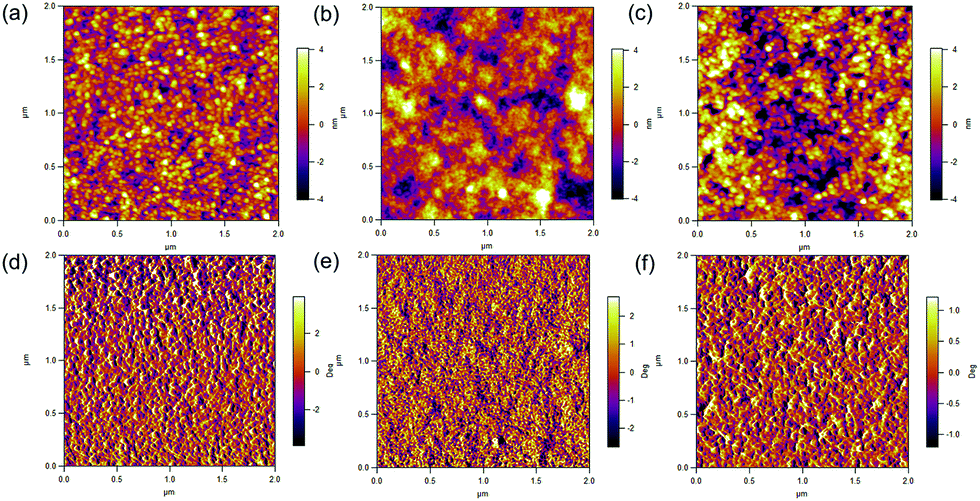 | ||
| Fig. 3 AFM surface topographic images (upper panels) and phase images (lower panels) of ZnO nanoparticle thin film on deposited on the ITO substrate (a and d); PTB7-Th:PC71BM active layer without (b and e) and with ZnO nanoparticle thin film (c and f) (image size: 2 μm × 2 μm). | ||
3.3 Mechanism study
The hole blocking mechanism by ZnO nanoparticle layers was investigated by hole-only diode measurements based on PTB7-Th:PC71BM blends with a structure of ITO/PEDOT:PSS/PTB7-Th:PC71BM (with or without) ZnO/MoOx/Au. With applied a positive bias, holes are injected from the MoOx/Au electrode via MoOx which has a deeper work function (5.4 eV) than that of PEDOT:PSS (5.2 eV). If the ZnO nanoparticle layer functions to block the holes, the current will be severely affected due to the formation of a non-ohmic contact. J–V characteristics of PTB7-Th:PC71BM hole-only diodes were fit by Mott–Gurney law (space-charge limited current model, or SCLC),35–37 as J = 9εrε0μ(V − Vbi)2/8L3, where εrε0 is the dielectric constant of the active layer, μ is the mobility, and L is the thickness of the active layer. As shown in Fig. 4a, the hole current of the device without the ZnO layer (plotted in a double log scale) shows a large range of quadratic dependence with a hole mobility of 5 × 10⁻⁸ m2 V−1 s−1 fitted by the SCLC model. In devices with ZnO nanoparticle layers, the hole current is dramatically reduced based on the same thickness of active layers and shows a limited range of quadratic voltage dependence. This is a fingerprint of forming injection limited current, attributed to the mismatch between the work functions. The decrease of hole current by nearly five orders of magnitude after incorporating the ZnO nanoparticle layer clearly demonstrates the effectiveness for the hole blocking functionality provided by ZnO nanoparticles. The improved hole block results in better selectivity of charge extraction at the cathode.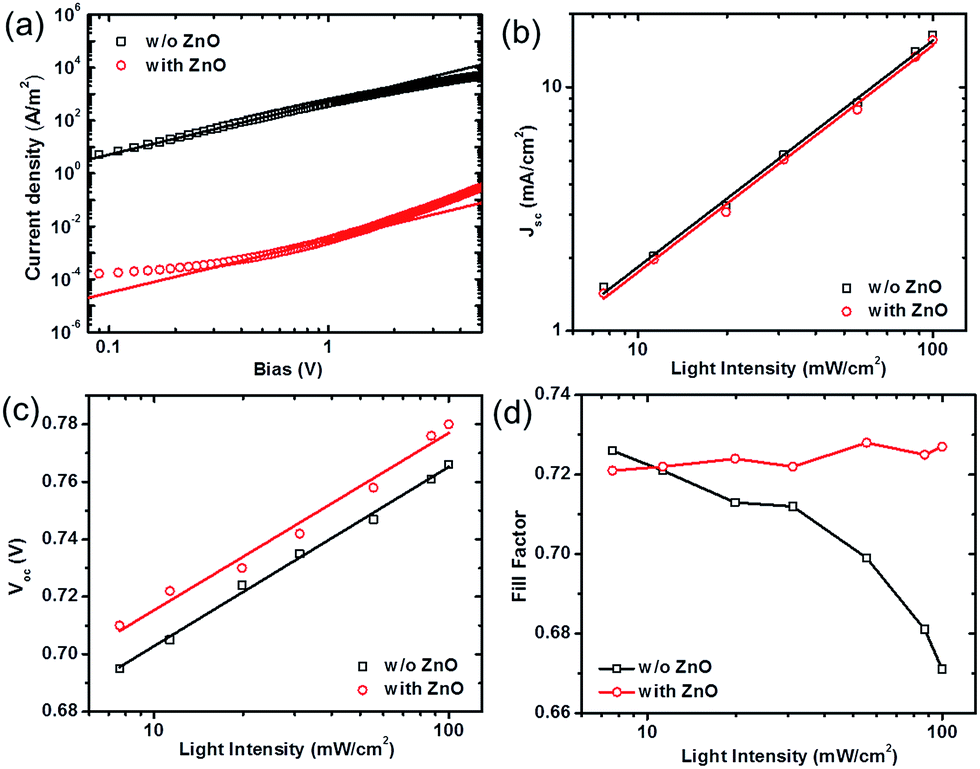 | ||
| Fig. 4 (a) J–V characteristics of hole-only devices in configuration of ITO/PEDOT:PSS/active layer/(ZnO)/MoOx/Au, the solid lines represent the best fit using the SCLC model. Irradiation intensity-dependence of (b) Jsc, (c) Voc, and (d) FF of PTB7-Th:PC71BM BHJ solar cells with and without ZnO nanoparticle layer. Solid lines in (b): power law fit; in (c): linear fit, and in (d): guide for eyes. | ||
We further studied the illumination intensity (I) dependence of solar cell device parameters without and with ZnO layers. A power law dependence of Jsc upon light intensity I is generally observed in BHJ solar cells as Jsc ∝ Iα, where α is the exponential factor.38,39 The slight deviation of α from unity arises from the weak bimolecular recombination in BHJ layers, while the value of α is close to 0.75 when monomolecular recombination fully limits the photocurrent.40 Jsc versus I characteristics for both devices without and with ZnO ETLs display α = 0.93 ± 0.02 in a plot with double-log scale, indicating the dominance of bimolecular charge recombination (Fig. 4b).
The plot of Voc versus I is a common method to qualitatively determine the recombination mechanism.41 Based on the metal–insulator–metal (MIM) model, the slope of Voc as a function log(I) equals the thermal voltage (kBT/e where e is the electron charge) when bimolecular recombination is dominant. When the slope exceeds kBT/e, trap assisted (Shockley–Read–Hall) charge recombination plays a role.42,43 As shown in Fig. 4c, the slope of the device with ZnO is 1.06 kBT/e, close to that for the device without ZnO (slope = 1.08 kBT/e); both are consistent with bimolecular recombination in PTB7-Th:PC71BM devices. Moreover, the observation that the slope is close to kBT/e also excludes the possibility of ZnO nanoparticles functioning as interfacial traps. On average the Voc of the device with ZnO ETLs is enhanced by 20 mV at all light intensities compared to that of the cell without ZnO. This can be a result of the suppression on the interfacial band bending near the cathode.
The functionality of ZnO layers is further clarified from the light intensity dependence of FF. Upon increasing light intensity, a higher density of charge carriers are generated in the photoactive layer and a slight increase in the recombination strength might be expected, which is likely to result in the decrease in FF.33 This trend is clearly observed in Fig. 4d for the device without ZnO. Interestingly, when incorporated with ZnO ETLs, the FF is noticeably enhanced under 100 mW cm−2 (1 sun), and also shows much weaker illumination intensity dependence in the range from 7 mW cm−2 to 100 mW cm−2. This indicates a possibility that the recombination strength might be decreased in devices with ZnO ETLs at higher light intensities near 1 sun.44
3.4 Device stability
At last, we examine the effect of ZnO nanoparticle ETLs on the device stability. Fig. 5a shows the PCEs versus device storage time in air of PTB7-Th:PC71BM solar cells without and with ZnO ETLs after encapsulation. For the device without ZnO ETLs, the PCE decreases almost 10% from 8.6% to 7.9% after 168 hours (seven days). The degradation of PTB7-Th:PC71BM solar cells is typically attributed to the photo-oxidation of organic layers or interfaces caused by the diffusion of molecular oxygen and water from atmosphere into the device even with encapsulation.45 After incorporated with ZnO ETLs (30 nm from 2ME:IPA solvent), the PCE has no observable decrease after one week storage in air. The FF for devices with ZnO ETLs remains above 72% after seven days, while in those devices without ZnO, the FF decreases from 68% to 64% after the same storage time (Fig. 5b). These results clearly demonstrate that ZnO nanoparticle layers improve the device stability of PTB7-Th:PC71BM solar cells.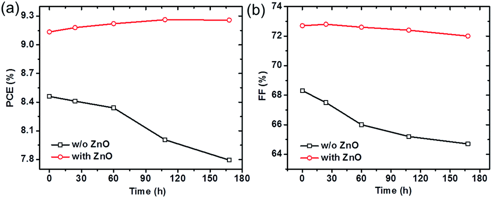 | ||
| Fig. 5 (a) PCE and (b) FF of PTB7-Th:PC71BM solar cells with and without ZnO nanoparticle ETLs as a function of device storage time. Solid lines are the guide for eyes. | ||
4. Conclusions
In conclusion, we have investigated the influences of processing and film thickness of ZnO nanoparticles ETLs on the device performance in polymer solar cells based on PTB7-Th:PC71BM and the origins for enhanced PCEs. The optimal ZnO HTLs are found to be around 30 nm when solution-processed from 2ME:IPA mixture solvents, leading to a best PCE = 9.2%. With conventional device structure, the device performance and stability of PTB7-Th:PC71BM solar cells are improved simultaneously after incorporating the ZnO nanoparticle ETL between the BHJ layer and Al cathode. The enhanced selectivity of charge extraction originates from the effectiveness in the hole blocking and exclusive charge extraction offered by the ZnO nanoparticle layer. Thereby the PCE is increased from 8.4% to 9.2% in the optimized condition with enlargement of Jsc and FF. The dense and air-stable ZnO nanoparticle thin films deposited on top of BHJ active layers function as an effective protection and thus enhance the device stability. Our results demonstrate a simple and versatile strategy to improve the performance of organic BHJ solar cells with superior air stability through interface engineering.Acknowledgements
H. Z. acknowledges the support from the Chinese Academy of Science (100 Top Young Scientists Program and QYZDB-SSW-SLH033). Y. Z. thanks ‘The 1000 Young Talents Program’ in China and the National Natural Science Foundation of China (No. 21674006). We greatly thank Prof. Alan J. Heeger in UCSB for the support and discussion on this work. We greatly thank Prof. Thuc-Quyen Nguyen at UCSB for helpful discussion on the manuscript. H. Z. thanks Dr Stephan Kraemer in UCSB for providing us with the TEM data.References
- G. Yu, J. Gao, J. C. Hummelen, F. Wudl and A. J. Heeger, Science, 1995, 270, 1789–1791 CAS.
- X. G. Guo, N. J. Zhou, S. J. Lou, J. Smith, D. B. Tice, J. W. Hennek, R. P. Ortiz, J. T. L. Navarrete, S. Y. Li, J. Strzalka, L. X. Chen, R. P. H. Chang, A. Facchetti and T. J. Marks, Nat. Photonics, 2013, 7, 825–833 CrossRef CAS.
- Z. B. Henson, K. Mullen and G. C. Bazan, Nat. Chem., 2012, 4, 699–704 CrossRef CAS PubMed.
- S. H. Park, A. Roy, S. Beaupre, S. Cho, N. Coates, J. S. Moon, D. Moses, M. Leclerc, K. Lee and A. J. Heeger, Nat. Photonics, 2009, 3, 297–302 CrossRef CAS.
- S. Li, L. Ye, W. Zhao, S. Zhang, S. Mukherjee, H. Ade and J. Hou, Adv. Mater., 2016, 28, 9423–9429 CrossRef CAS PubMed.
- Z. Li, K. Jiang, G. Yang, J. Y. L. Lai, T. Ma, J. Zhao, W. Ma and H. Yan, Nat. Commun., 2016, 7, 13094 CrossRef CAS PubMed.
- Y. Lin, F. Zhao, Y. Wu, K. Chen, Y. Xia, G. Li, S. K. K. Prasad, J. Zhu, L. Huo, H. Bin, Z.-G. Zhang, X. Guo, M. Zhang, Y. Sun, F. Gao, Z. Wei, W. Ma, C. Wang, J. Hodgkiss, Z. Bo, O. Inganäs, Y. Li and X. Zhan, Adv. Mater., 2017, 29, 1604155 CrossRef PubMed.
- J. Peet, J. Y. Kim, N. E. Coates, W. L. Ma, D. Moses, A. J. Heeger and G. C. Bazan, Nat. Mater., 2007, 6, 497–500 CrossRef CAS PubMed.
- J. Jo, S. S. Kim, S. I. Na, B. K. Yu and D. Y. Kim, Adv. Funct. Mater., 2009, 19, 866–874 CrossRef CAS.
- E. Verploegen, R. Mondal, C. J. Bettinger, S. Sok, M. F. Toney and Z. A. Bao, Adv. Funct. Mater., 2010, 20, 3519–3529 CrossRef CAS.
- K. Lee, J. Y. Kim, S. H. Park, S. H. Kim, S. Cho and A. J. Heeger, Adv. Mater., 2007, 19, 2445–2449 CrossRef CAS.
- H. Q. Zhou, N. E. Coates, G. Hernandez-Sosa and D. Moses, Adv. Funct. Mater., 2012, 22, 3279–3283 CrossRef CAS.
- L. M. Chen, Z. Xu, Z. R. Hong and Y. Yang, J. Mater. Chem., 2010, 20, 2575–2598 RSC.
- C. J. Brabec, S. Gowrisanker, J. J. M. Halls, D. Laird, S. J. Jia and S. P. Williams, Adv. Mater., 2010, 22, 3839–3856 CrossRef CAS PubMed.
- R. Steim, F. R. Kogler and C. J. Brabec, J. Mater. Chem., 2010, 20, 2499–2512 RSC.
- M. J. Tan, S. Zhong, J. Li, Z. Chen and W. Chen, ACS Appl. Mater. Interfaces, 2013, 5, 4696–4701 CAS.
- G. Long, X. Wan, B. Kan, Z. Hu, X. Yang, Y. Zhang, M. Zhang, H. Wu, F. Huang, S. Su, Y. Cao and Y. Chen, ChemSusChem, 2014, 7, 2358–2364 CrossRef CAS PubMed.
- L. K. Jagadamma, H. Hu, T. Kim, G. O. N. Ndjawa, A. E. Mansour, A. El Labban, J. C. D. Faria, R. Munir, D. H. Anjum, M. A. McLachlan and A. Amassian, Nano Energy, 2016, 28, 277–287 CrossRef CAS.
- J. Zhao, Y. Li, G. Yang, K. Jiang, H. Lin, H. Ade, W. Ma and H. Yan, Nature Energy, 2016, 1, 15027 CrossRef CAS.
- J. Xiong, J. Yang, B. Yang, C. Zhou, X. Hu, H. Xie, H. Huang and Y. Gao, Org. Electron., 2014, 15, 1745–1752 CrossRef CAS.
- Y.-A. Su, W.-C. Lin, H.-J. Wang, W.-H. Lee, R.-H. Lee, S. A. Dai, C.-F. Hsieh and R.-J. Jeng, RSC Adv., 2015, 5, 25192–25203 RSC.
- Z.-L. Tseng, C.-H. Chiang, S.-H. Chang and C.-G. Wu, Nano Energy, 2016, 28, 311–318 CrossRef CAS.
- A. K. K. Kyaw, D. H. Wang, D. Wynands, J. Zhang, T.-Q. Nguyen, G. C. Bazan and A. J. Heeger, Nano Lett., 2013, 13, 3796–3801 CrossRef CAS PubMed.
- J. B. You, C. C. Chen, L. T. Dou, S. Murase, H. S. Duan, S. A. Hawks, T. Xu, H. J. Son, L. P. Yu, G. Li and Y. Yang, Adv. Mater., 2012, 24, 5267–5272 CrossRef CAS PubMed.
- Y. M. Sun, J. H. Seo, C. J. Takacs, J. Seifter and A. J. Heeger, Adv. Mater., 2011, 23, 1679–1683 CrossRef CAS PubMed.
- L. Qian, Y. Zheng, J. G. Xue and P. H. Holloway, Nat. Photonics, 2011, 5, 543–548 CrossRef CAS.
- Z. H. Lin, J. J. Chang, C. Y. Jiang, J. Zhang, J. S. Wu and C. X. Zhu, RSC Adv., 2014, 4, 6646–6651 RSC.
- C. L. Chochos, N. Tagmatarchis and V. G. Gregoriou, RSC Adv., 2013, 3, 7160–7181 RSC.
- W. J. E. Beek, M. M. Wienk, M. Kemerink, X. N. Yang and R. A. J. Janssen, J. Phys. Chem. B, 2005, 109, 9505–9516 CrossRef CAS PubMed.
- W. W. Li, A. Furlan, K. H. Hendriks, M. M. Wienk and R. A. J. Janssen, J. Am. Chem. Soc., 2013, 135, 5529–5532 CrossRef CAS PubMed.
- M. V. Kovalenko, M. Scheele and D. V. Talapin, Science, 2009, 324, 1417–1420 CrossRef CAS PubMed.
- E. H. Sargent, Nat. Photonics, 2009, 3, 325–331 CrossRef CAS.
- N. E. Coates, H. Q. Zhou, S. Kramer, L. A. Li and D. Moses, Adv. Mater., 2010, 22, 5366–5369 CrossRef CAS PubMed.
- W. L. Ma, S. L. Swisher, T. Ewers, J. Engel, V. E. Ferry, H. A. Atwater and A. P. Alivisatos, ACS Nano, 2011, 5, 8140–8147 CrossRef CAS PubMed.
- Y. Zhang and P. W. M. Blom, Appl. Phys. Lett., 2010, 97, 083303 CrossRef.
- Y. Zhang and P. W. M. Blom, Appl. Phys. Lett., 2011, 98, 143504 CrossRef.
- V. D. Mihailetchi, J. Wildeman and P. W. M. Blom, Phys. Rev. Lett., 2005, 94, 126602 CrossRef CAS PubMed.
- I. Riedel, J. Parisi, V. Dyakonov, L. Lutsen, D. Vanderzande and J. C. Hummelen, Adv. Funct. Mater., 2004, 14, 38–44 CrossRef CAS.
- V. D. Mihailetchi, L. J. A. Koster, J. C. Hummelen and P. W. M. Blom, Phys. Rev. Lett., 2004, 93, 216601 CrossRef CAS PubMed.
- V. D. Mihailetchi, H. X. Xie, B. de Boer, L. J. A. Koster and P. W. M. Blom, Adv. Funct. Mater., 2006, 16, 699–708 CrossRef CAS.
- L. J. A. Koster, V. D. Mihailetchi, R. Ramaker and P. W. M. Blom, Appl. Phys. Lett., 2005, 86, 123509 CrossRef.
- S. R. Cowan, A. Roy and A. J. Heeger, Phys. Rev. B: Condens. Matter Mater. Phys., 2010, 82, 245207 CrossRef.
- M. M. Mandoc, W. Veurman, L. J. A. Koster, B. de Boer and P. W. M. Blom, Adv. Funct. Mater., 2007, 17, 2167–2173 CrossRef CAS.
- L. J. A. Koster, V. D. Mihailetchi and P. W. M. Blom, Appl. Phys. Lett., 2006, 88, 052104 CrossRef.
- M. Jørgensen, K. Norrman, S. A. Gevorgyan, T. Tromholt, B. Andreasen and F. C. Krebs, Adv. Mater., 2012, 24, 580–612 CrossRef PubMed.
Footnote |
| † Electronic supplementary information (ESI) available. See DOI: 10.1039/c6ra28246f |
| This journal is © The Royal Society of Chemistry 2017 |