
 Open Access Article
 This Open Access Article is licensed under a
 Creative Commons Attribution 3.0 Unported Licence
Flexible micro-supercapacitors prepared using direct-write nanofibers†
Caiwei Shen *a,
Chun-Ping Wangb,
Mohan Sanghadasac and
Liwei Lina
*a,
Chun-Ping Wangb,
Mohan Sanghadasac and
Liwei Lina
aDepartment of Mechanical Engineering, University of California at Berkeley, 1113 Etcheverry Hall, Berkeley, CA 94720, USA. E-mail: shencw10@berkeley.edu; Tel: +1-5106428983
bDepartment of Power Mechanical Engineering, National Tsing Hua University, Hsinchu, Taiwan
cAviation and Missile Research, Development, and Engineering Center, US Army, Redstone Arsenal, AL, USA
First published on 16th February 2017
Abstract
Herein, we demonstrated direct-write flexible micro-supercapacitors prepared by the near-field electrospinning of polypyrrole (PPy) nanofibers on a patterned metal electrode deposited on a flexible polymer substrate. The continuous porous nanofiber network with a pseudocapacitance effect greatly increases the capacitance and facilitates ion transport in the electrodes. The prototype based on the lab-synthesized PPy nanofibers shows a high capacitance of 0.48 mF cm−2 when the total area of both electrodes and electrolyte is considered, and the performance is not affected when it is bent to different extents. The micro-supercapacitors were experimentally proved to be highly flexible with excellent electrochemical performance and cycling stability. Our approach is simple, versatile, and compatible with different substrates for the direct integration of energy storage devices in flexible microsystems.
1. Introduction
The possibility of harvesting and storing energy from the environment has attracted significant interest in emerging microelectronic systems such as wearable electronics, implantable medical devices, and active radio frequency identification (RFID). Since the energy harvested from solar, thermal, or mechanical sources and the power consumption of the electronics are mostly in an intermittent manner, the energy storage units are indispensable in storing electricity from the energy harvesters. Although rechargeable batteries and supercapacitors are the most common solutions, batteries suffer from intrinsic problems such as short cycle life, low-power density, and have safety concerns. Supercapacitors, on the other hand, are safer in operation with longer cycle life and higher charge/discharge rates.1–4Two types of supercapacitor have been categorized by the charge storage mechanisms.1,5 One is based on the electrical double layer (EDL) effect, which stores static charges on the interface between an electrode and an ion-containing electrolyte. The capacitance of an EDL capacitor is highly dependent on the accessible surface area of the electrode material. The other type known as pseudocapacitor relies on fast and reversible redox reactions that occur at the surface of the active materials. Transition metal oxides and electronically conducting polymers are generally used in pseudocapacitors and show specific capacitances exceeding those of the EDL capacitors. Since pseudocapacitors store charge only in the first few nanometers from the surface, nanostructures with a high surface area also help to improve the active material usage and accordingly increase the capacitance.1
To apply high-performance supercapacitor materials to energy storage devices in microsystems, considerations on both material synthesis and device fabrication are required. Desirable characteristics of these supercapacitors include (1) small size compatibility with other components, (2) low manufacturing costs with the possibility to be directly integrated with the rest of the system, and (3) good flexibility to fit in with different form-factors, especially for applications in flexible systems.
On-chip micro-supercapacitors, especially carbon-based EDL capacitors, have been demonstrated using various technologies, including chemical vapor deposition (CVD) used for the direct growth of CNTs,6–10 carbide-derived carbon,11–13 silicon nanowires,14 silicon carbide nanowires,15 and carbonization used for the synthesis of patterned micro-sized carbon electrodes with nanopores,16,17 to grow the active materials. Some of these supercapacitor electrodes have been constructed on silicon wafers for the possible integration with microelectronics. However, the typical high temperature process requirements in constructing these nanostructures prevent their direct integration with silicon-based devices. Electrophoresis has been used to assemble onion-like carbon particles to form interdigital electrodes with ultra-high power;18 however, it involves a wet process, which also limits the direct integration process when immersing the substrates in complex electrolytes. Similar issues are encountered when developing pseudocapacitors on a chip by evaporation,19 chemical growth20 or electrochemical deposition.21,22 Printing of nanostructured carbon particles23 and laser writing of graphene,24–26 on the other hand, have shown good possibility of fabricating micro-supercapacitors on flexible substrates for EDL capacitors without the capability of constructing pseudocapacitors with higher capacitance.
Herein, we proposed and demonstrated the direct-write flexible micro-supercapacitors using near-field electrospinning of polypyrrole nanofibers. The continuous nanofiber network with high surface area is ultra-flexible and makes full use of the active material for high pseudocapacitance. The direct-write process performed at room temperature does not involve wetting of the substrate. Moreover, it is simple, low-cost, and applicable to arbitrary flexible surfaces for the possible direct integration with other devices and systems.
2. Experimental
2.1 Design
Conducting polymers, such as polypyrrole, poly(3,4-ethylenedioxythiophene), and polyaniline, is a group of polymers that conduct electrons when they are doped.27 They can work as pseudocapacitive materials to store energy via a doping/de-doping (charging/discharging) effect in ion-containing electrolytes. Conducting-polymer-based supercapacitors show much higher specific capacitances than EDL capacitors. Their power densities and cycling capabilities, on the other hand, can be improved using appropriate nanostructures that reduce ion diffusion within the electrode material.27–29Electrospinning is a simple and versatile technique to generate continuous fibers with diameters from sub-micron to nanometers.30,31 Different types of functional fibers, most of which are made of chain polymers, can be produced by electrospinning as long as a uniform solution with an appropriate viscosity and surface tension can be prepared. We applied near-field electrospinning (NFES),31,32 in which the electrode-to-collector distance was only 0.5–5 mm, to directly write conducting polymer nanofibers on flexible substrates. The electrospun conducting polymer nanofibers can enhance the performance of supercapacitor electrodes because the continuous nanoporous network provides a large surface area that ensures the full use of active material and facilitates ion transport and diffusion in the electrode. Moreover, a micro-energy storage device can be easily integrated with other flexible and miniaturized systems since NFES can orderly deposit nanofibers onto micro-sized patterns on arbitrary surfaces, as illustrated in Fig. 1a.
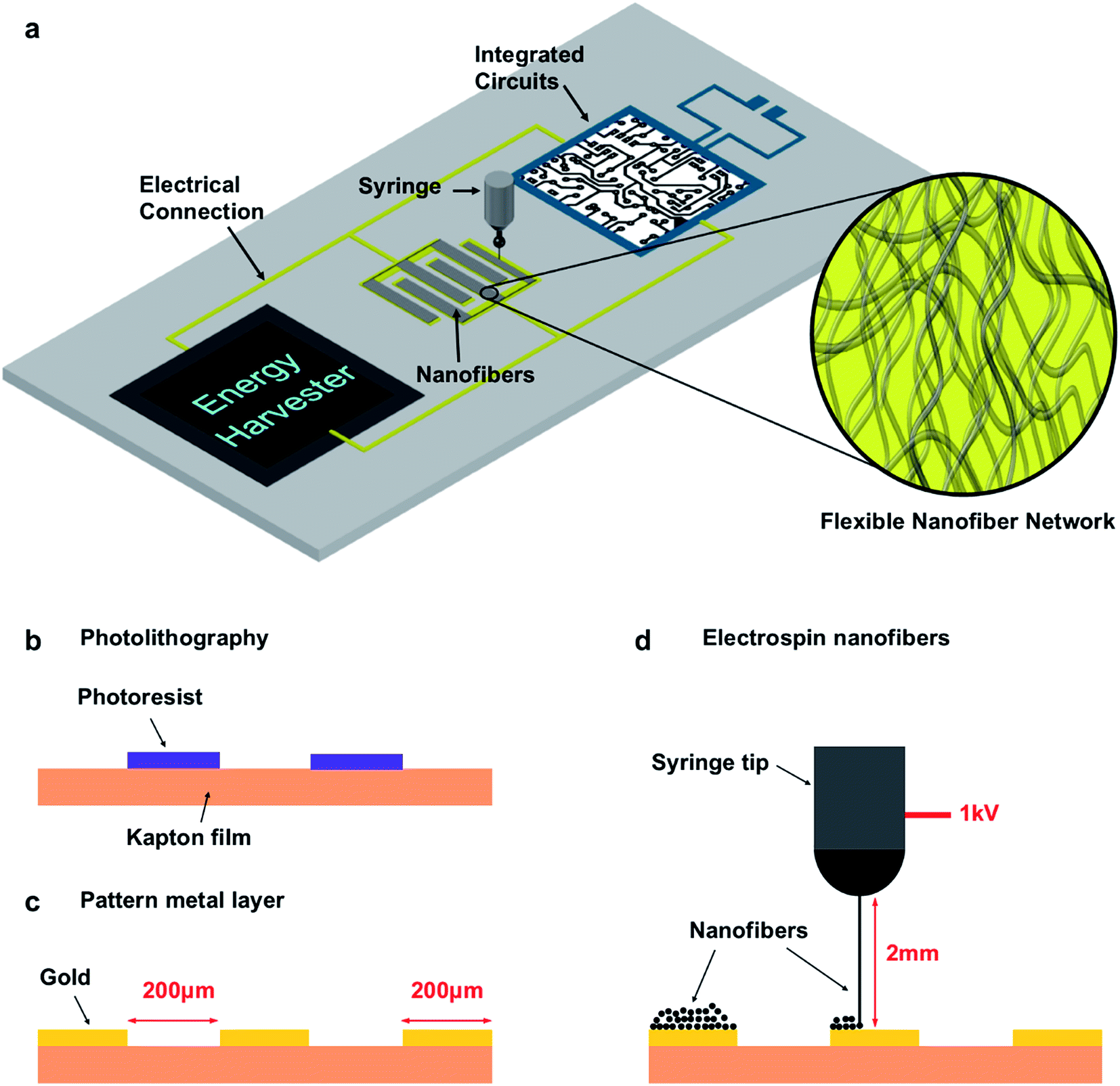 | ||
| Fig. 1 (a) Schematic of the direct writing of a nanofiber-based micro-supercapacitor on an arbitrary substrate to integrate with an energy harvester and other circuits. A flexible nanofiber network was locally deposited on the metal electrodes with micro-sized patterns using near-field electrospinning. (b)–(d) Cross-section schematic of the fabrication process. (b) Patterning of the photoresist on the flexible substrate by photolithography. (c) Patterning of the electrodes by the deposition of gold and the removal of the photoresist. (d) Writing of the nanofibers onto the electrodes using NFES. | ||
2.2 Material preparation
In this study, polypyrrole (PPy) was used as the active material for micro-supercapacitors because it has high theoretical capacitance and high conductivity.27 As the electrospinning process requires the active material to be contained in a uniform solution, PPy, which can be dissolved in organic solvents, was synthesized using a modified process developed by Oh et al.33 Typically, 8.05 g of pyrrole monomer was mixed with 26.67 g of docusate sodium salt in 180 mL of deionized water to form solution A, whereas 4.01 g of ammonium persulfate was dissolved in 20 mL of deionized water to form solution B. Both solutions were cooled down to 0 °C and solution B was slowly added to solution A under stirring. The reaction mixture was kept at 0 °C under continuous stirring for 24 h. PPy precipitated and the precipitate was then filtered and washed several times with methanol and water. After drying under vacuum for 12 h, the PPy powder was collected and dissolved in dimethylformamide (DMF) to form 8 wt% solution for the following process.To prepare the lab-synthesized PPy for the NFES process, polyethylene oxide (PEO, Mw ∼ 5![[thin space (1/6-em)]](https://www.rsc.org/images/entities/char_2009.gif) 000000) was used to adjust the viscosity and surface tension of the solution. In a typical process, PEO was dissolved in a solvent (DMF:acetone = 2:3) mixture to make 2 wt% solution. The 8 wt% PPy solution was then mixed with the PEO solution such that the weight ratio of PPy and PEO was 1:1 in the final solution.
000000) was used to adjust the viscosity and surface tension of the solution. In a typical process, PEO was dissolved in a solvent (DMF:acetone = 2:3) mixture to make 2 wt% solution. The 8 wt% PPy solution was then mixed with the PEO solution such that the weight ratio of PPy and PEO was 1:1 in the final solution.
Since the properties of the conducting polymer vary a lot when using different synthetic processes, we also examined a commercially available PPy product as a control in our experiments. The PPy dispersion (5 wt% in water) was supplied from Sigma-Aldrich and was mixed with PEO (Mw ∼ 300000) and Triton X-100 in this case. Typically, 0.5 g of PEO was dissolved in 2 g of deionized water and stirred for 3 h. Then, 5 g of the PPy suspension and 0.25 g of Triton were added to the solution and stirred overnight.
2.3 Device fabrication
Kapton® polyimide film was used as a flexible plastic substrate. The cross-section view of the fabrication process of the micro-supercapacitor prototype is illustrated in Fig. 1b–d. The photoresist was first spin-coated and patterned by photolithography (Fig. 1b). Then, a 100 nm thick layer of gold was thermally evaporated onto the substrate and an additional photoresist was removed using a lift-off process to construct the interdigital electrodes (Fig. 1c). The metal layer was much more conductive than the functional polypyrrole and served as the current collector to improve the overall performance of the device. This layer is also required for an electrical connection with other components in an integrated microsystem and it does not increase the complexity of the whole system. The NFES process was followed to deposit the functional nanofibers onto the electrodes, during which the substrate was fixed on a computer-controlled X–Y motion stage. The polymer solution, either the one with commercial PPy dispersion or the one with lab-synthesized PPy, was filled into a syringe equipped with a 22 gauge flat-end needle. The syringe was placed 2 mm above the gold pattern and the needle was connected to a high voltage source with the gold electrode grounded. By tuning the output voltage at around 1 kV, nanofibers were pulled out of the tip from the viscous solution in the syringe via an electrostatic force and fall onto the grounded electrodes. The motion stage was pre-programmed during the process to write the nanofibers on the interdigital patterns (Fig. 1d).Fig. 2a shows an optical image of the electrode pattern. Each gold finger in the pattern was 200 μm wide and 1300 μm long with a 200 μm wide gap in between. The total area of the comb-shaped interdigital electrodes was 2.2 mm × 1.9 mm. Fig. 2b and c show the microscopic images of an electrode finger before and after the NFES process. It can be seen that the gold surface was uniformly covered with the nanofibers after the electrospinning process. The SEM image in Fig. 2d shows a 1 μm thick layer of nanofibers, with an average diameter of 200 nm, electrospun from the commercial PPy dispersion on a Si wafer. The samples on a plastic substrate, however, displayed a poor SEM image because of the low conductivities of both the substrate and the commercial PPy material. In the prototype that we used to test the electrochemical performance, the thickness of the nanofiber network was about 5 μm. Fig. 2e shows the SEM image of the nanofibers, with an average diameter of 700 nm and an average thickness of about 5 μm, constructed from the lab-synthesized PPy on a plastic substrate. The image quality was better in this case since the conductivity of the lab-synthesized PPy was higher and the nanofibers were thicker. Nano-sized roughness was seen on the surface of the nanofibers and it helped to increase the total surface area of the network. The diameter of the nanofibers can be tuned by adjusting the viscosity and surface tension of the polymer solution, as well as the NFES parameters such as the voltage and tip-to-substrate distance. For example, nanofibers that were 300 ± 100 nm in diameter were spun from the solution in which the weight ratio of the lab-synthesized PPy and PEO was 7:3 (ESI Fig. S1a†). However, the electrospinning process of this solution was not stable and the nanofibers tended to aggregate on random locations of the metal electrodes (ESI Fig. S1b†). Thicker nanofibers with diameters of 1500 ± 500 nm were spun from a more viscous solution (PPy:PEO = 4:6, ESI Fig. S1c†). These nanofibers were sparsely distributed on the metal electrodes and resulted in a relatively low capacitance (ESI Fig. S1d†). The optimized process resulted in nanofibers that were uniformly deposited on the metal electrodes, as indicated by Fig. 2c and e, and were considered as the most reliable conditions for the deposition of the lab-synthesized PPy.
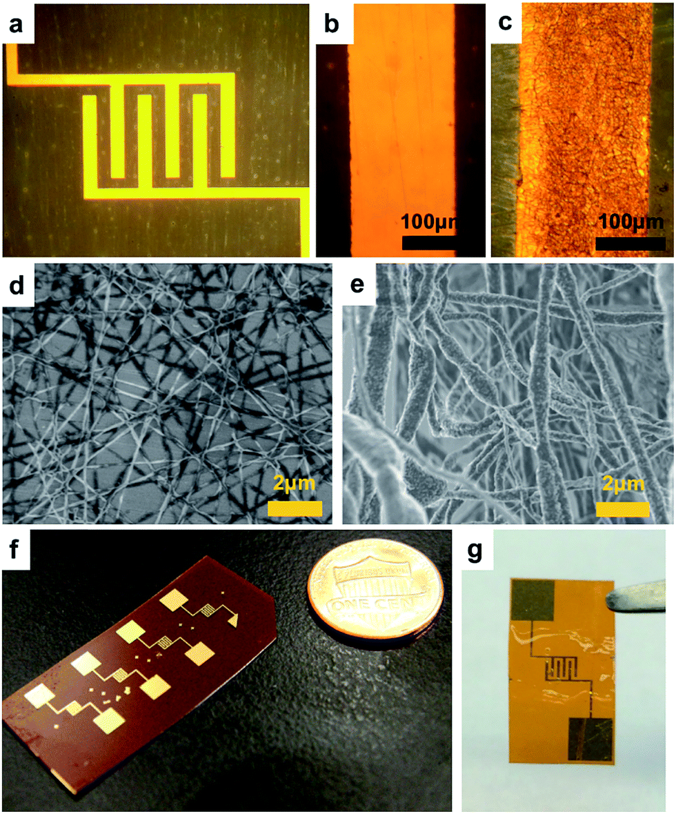 | ||
| Fig. 2 Optical images of the (a) comb-shaped interdigital gold electrodes, (b) blank electrode surface, and (c) electrode covered by the electrospun nanofibers. Scanning electron microscopy (SEM) images of the (d) electrospun nanofibers of commercial PPy and (e) electrospun nanofibers of the lab-synthesized PPy. Optical images of (f) the multiple micro-supercapacitor cells on a piece of plastic substrate and on a one-cent US coin in the background and (g) a prototype with a thin layer of polymer electrolyte. | ||
Fig. 2f shows an image of the plastic substrate with multiple cells of micro-supercapacitor on it. The fabrication process is applicable to various substrates with larger arrays, even substrates with other components on them, as illustrated in Fig. 1a. To test the electrochemical performance of the prototype, a solid-state polymer electrolyte was applied to complete the device. The electrolyte was prepared by first dissolving 1 g of polyvinyl alcohol (PVA, Mw ∼ 90000) in 8 g of deionized water at 80 °C under stirring until it a clear solution was formed, and then 1 g of 85 wt% H3PO4 was added to the solution. The solution was applied onto the active electrode area and dried in the air. Fig. 2g shows a complete prototype ready for testing, where a thin and transparent layer of polymer electrolyte covers the electrode area. Three types of cells were prepared for comparison: a blank cell without nanofibers on the gold electrodes, a cell with nanofibers of commercial PPy, and a cell with nanofibers of the lab-synthesized PPy.
3. Results and discussion
The supercapacitors performance was characterized using a Gamry Reference 600 potentiostat. Fig. 3a and b show the cyclic voltammetry (CV) curves of the prototypes using commercial PPy and lab-synthesized PPy, respectively. Both cells show capacitive energy storage behavior as indicated by the symmetric parallelogram shapes under different scan rates and the increase in the current with the scan rate. Since the devices were charged and discharged at a higher rate when the scan rate was higher, the excellent capacitive performances preserved at 1 V s−1 imply their potential applications for fast charge and discharge systems. Fig. 3c compares the CV curves obtained for the three cells at the same scan rate of 20 mV s−1. The blank cell shows a small current caused by the electrical double layer effect of the gold layer. The prototypes with nanofibers have a much larger current density than the blank cell, which proves that their supercapacitor performance was mainly contributed by the electrospun nanofibers instead of the gold electrodes. Moreover, the cell prepared using the lab-synthesized PPy shows a obviously larger current than the others, indicating its larger capacity.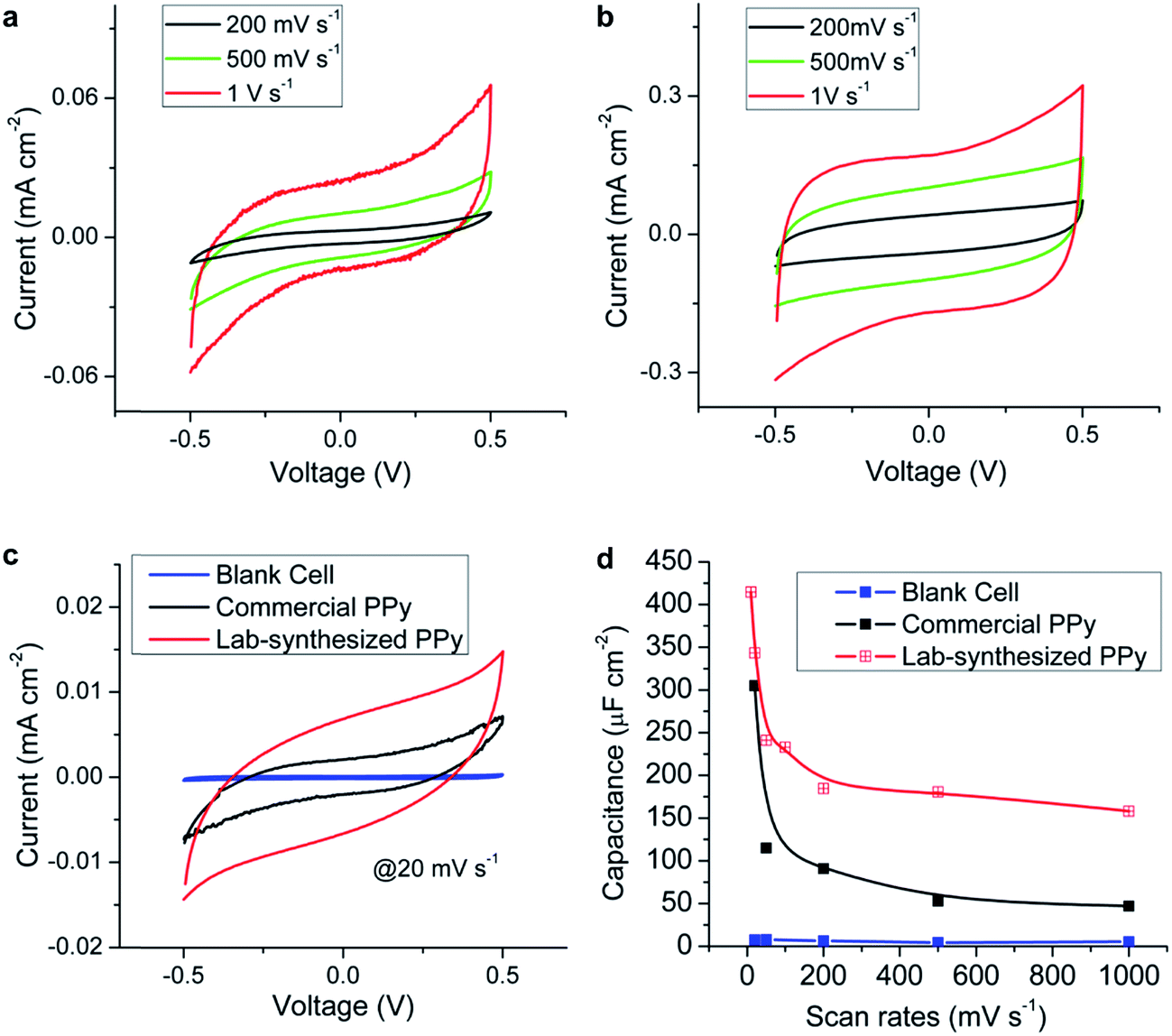 | ||
| Fig. 3 Cyclic voltammetry curves obtained for the micro-supercapacitor cells using the (a) commercial PPy-based nanofibers and (b) lab-synthesized PPy-based nanofibers at different scan rates. (c) A comparison of the CV curves obtained for the three cells at the same scan rate of 20 mV s−1. (d) The calculated areal capacitances of the three cells versus the scan rate. | ||
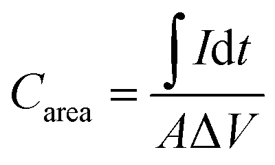
The capacitances per unit area of the devices can be calculated from the CV curves using the following formula:
 | (1) |
On the other hand, a number of studies have demonstrated that the performance, including the capacitance and power per unit area, can also be improved by improving the design of the electrode sizes and increasing the thickness of the functional materials.35,36 The capacity of the prototype characterized in this study can also be directly increased by repeating the NFES process, i.e. by depositing a thicker layer of nanofibers. Our current experimental setup allows a uniform deposition of an up to 5 μm-thick nanofiber network onto 200 μm-wide electrodes. This is because the control precision of the motion stage limits the writing precision and the nanofibers may not fall onto the exact position when the writing is repeated multiple times. However, thicker layers are still achievable on wider electrodes with the same setup.
We have also conducted bending tests of the prototypes to evaluate their flexibility. The images shown in Fig. 4a–c represent the bending conditions, in which the prototype was kept straight, bent forward, and bent backward, respectively. Cyclic voltammetry curves for the two cells with nanofibers were obtained at each bending state, as shown in Fig. 4d and e. The curves show that the performance of both prototypes doesn't significantly change when they are bent. For the cell using the commercial PPy, a minor drop in the current occurs when it is bent backward. This phenomenon doesn't happen in the case of the other cell using the lab-synthesized PPy, which shows almost exactly the same performance under different bending states. The reason for the slightly different responses is mainly due to the surface properties of the nanofibers. The commercial PPy is hydrophilic such that the nanofibers attach to the electrolyte layer better than the substrate. A small portion of the nanofibers loses contact with the gold electrode when the device is bent backward and the electrolyte layer is stretched. As a result, the testing current drops because less electrode material is connected to the metal layer. The lab-synthesized PPy, however, is well bonded to the gold electrode and is not affected by the bending and deformation of the solid electrolyte. Both nanofibers are ultra-flexible due to the nature of the 1D nanostructures, which make them suitable as functional materials for applications in flexible systems.
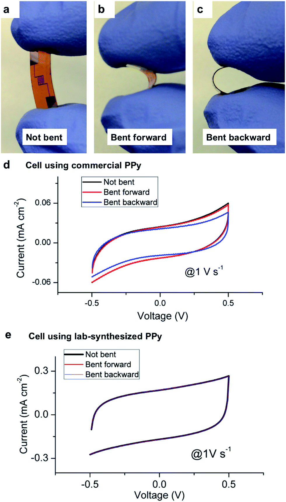 | ||
| Fig. 4 Images of the micro-supercapacitor with electrodes facing left when it's (a) straight, (b) bent forward, and (c) bent backward. The bending radius of the curvature was kept at 3 mm during all the tests. Cyclic voltammetry curves obtained for the cells using the (d) commercial PPy-based nanofibers and (e) lab-synthesized PPy-based nanofibers when they are bent in different directions. | ||
Further characterization, including a constant current charge–discharge test, impedance measurements, and cycling tests, of the prototypes using the lab-synthesized PPy were conducted and the results are summarized in Fig. 5. Cyclic voltammetry curves at low scan rates were investigated from 0 to 1 V, as shown in Fig. 5a. The capacitive behavior still dominates at 2 mV s−1 and no battery-like redox reactions are observed in the curves. Fig. 5b shows the charge–discharge curves obtained for the prototype under constant currents from 5 to 50 μA cm−2. The nearly straight lines also indicate the excellent capacitive behavior of the device. The internal resistance was estimated to be 3.1 ± 0.1 kΩ cm2 from the IR drops of the curves. A capacitance of 0.48 mF cm−2 was calculated at a charging current of 5 μA cm−2, which was slightly higher than the value obtained from the cyclic voltammetry curves (0.42 mF cm−2). A volumetric capacitance of 0.96 F cm−3 was derived if the thickness of the electrodes was considered. Most of the micro-supercapacitors reported in the literature show areal capacitances between 0.1 and 10 mF cm−2 and volumetric capacitances between 0.1 and 10 F cm−3.37 In addition to our nanofiber-based electrodes, various studies have reported the use of 1D nanomaterials to build 3D porous networks for on-chip energy storage because these structures offer an easily accessible high surface area. Most of these, such as SiC nanowires (0.24 mF cm−2, or 0.24 F cm−3)15 and carbon nanotube forests (0.428 mF cm−2, or 0.053 F cm−3),6 are based on EDL capacitance only. Our capacitance was relatively high when compared to these structures with similar porosity because the EDL and the pseudocapacitance effect co-exist in the PPy nanofibers. Some 2D structured materials, such as laser written graphene oxide (0.106 mF cm−2, or 0.479 F cm−3),26 are also used as a micro-supercapacitor and the capacitance was also limited by the single EDL effect. Besides the EDL capacitors, our prototype shows better flexibility and areal capacitance than some pseudocapacitors using rigid materials. For example, in a MnOx/Au supercapacitor (0.39 mF cm−2),19 very thin 2D MnOx/Au layers have to be used to improve the conductivity and retain the flexibility of the electrodes.
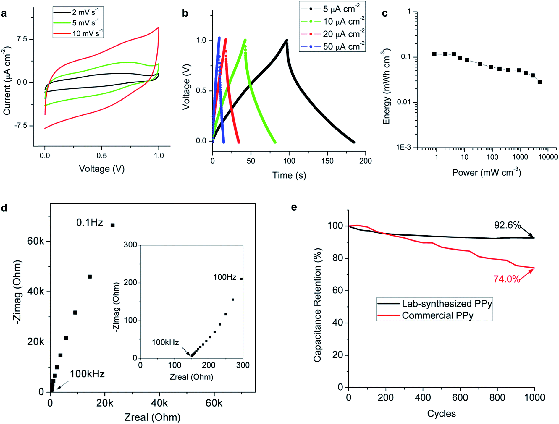 | ||
| Fig. 5 Further characterization of the micro-supercapacitor using lab-synthesized PPy. (a) Cyclic voltammetry curves obtained at low scan rates within the 1 V range. (b) Constant current charge–discharge curves. (c) Calculated energy density versus power density. (d) Nyquist plot showing the impedance spectrum. Inset shows the zoom-in view of the impedance spectrum in the high frequency region. (e) Cycling tests of the cells using the different active materials, in which the cells were charged and discharged for 1000 cycles at a scan rate of 100 mV s−1 from 0 to 1 V. | ||
The energy densities and power densities of the prototype were calculated and are plotted in Fig. 5c, in which the points are derived from the cyclic voltammetry tests performed at different scan rates. For most micro-supercapacitors, energy densities have been reported between 0.01 and 10 mW h cm−3.37,38 Our device shows the ability to uptake/deliver a wide range of power densities with the energy densities around 0.1 mW h cm−3. Considering that the fabrication method is simple, versatile, and avoids high temperature and processes that immerse the substrates in complex solutions, our direct-write micro-supercapacitor is promising for applications in a self-powered integrated system such as that illustrated in Fig. 1a. Usually, a microelectromechanical system (MEMS)-based energy harvester generates a power density smaller than 1 mW cm−3,39 and it is difficult to constantly power a wireless sensor node. Our micro-supercapacitor with comparable size was able to store this generated power and provide higher power to sensors or transmitters when necessary.
Fig. 5d shows the Nyquist plot of the impedance, which shows the capacitive behavior of the device over a large frequency range. The crossover frequency at the phase angle of −45° was about 60 Hz, which is even higher than that of the micro-supercapacitors based on highly conductive graphene.25,40 The excellent frequency response was attributed to the fast ion transport within the porous nanofiber network, which is also proved by the absence of a semi-circle in the Nyquist plot in the high frequency region.
One drawback of the typical conducting polymer-based supercapacitors is their poor cycling stability caused by the insertion/de-insertion of ions in the polymer matrix. The use of nanostructures can greatly improve the stability because of the shortened transport distances within the material. Fig. 5e shows the cycling experimental results and the calculated relative capacitances of the prototypes using different active materials for 1000 cycles. The capacitance retention is 92.6% after 1000 cycles for the lab-synthesized PPy, indicating excellent stability for a pseudocapacitor based on fast redox reactions.
4. Conclusions
We successfully demonstrated a solid-state flexible micro-supercapacitor based on polymer nanofibers. The nanofibers can be directly written onto micro-sized electrode patterns on various substrates including flexible polymer films. Characterization of the prototypes shows that the nanofiber network exhibits a two orders of magnitude increase in capacitance when compared with a flat electrode surface. The nanostructure also benefits the power performance and frequency response of the device by facilitating ion transport within the porous electrode. The prototype based on the lab-synthesized PPy nanofibers show a high capacitance of up to 0.48 mF cm−2 and the same performance when it is bent at different states. Overall, the micro-supercapacitor was highly flexible with excellent electrochemical performance and cycling stability. Our approach is simple, versatile, and compatible with different substrates for the direct integration of energy storage devices in flexible microsystems.Acknowledgements
This work was supported in part by the BSAC, Berkeley Sensor and Actuator Center, the National Science Foundation Industry/University Cooperative Research Center, and the US Army Aviation and Missile Research, Development and Engineering Center.References
- P. Simon and Y. Gogotsi, Nat. Mater., 2008, 7, 845–854 CrossRef CAS PubMed
.
- M. Armand and J.-M. Tarascon, Nature, 2008, 451, 652–657 CrossRef CAS PubMed
- A. Burke, Electrochim. Acta, 2007, 53, 1083–1091 CrossRef CAS
- J. R. Miller and P. Simon, Science, 2008, 321, 651–652 CrossRef CAS PubMed
- B. E. Conway, Electrochemical Supercapacitors, Springer, US, Boston, MA, 1999 Search PubMed
- Y. Q. Jiang, Q. Zhou and L. Lin, 22nd IEEE Int. Conf. Micro Electro Mech. Syst., 2009, 587–590 Search PubMed
- Y. Jiang and L. Lin, Sens. Actuators, A, 2012, 188, 261–267 CrossRef CAS
- Y. Jiang, P. Wang, X. Zang, Y. Yang, A. Kozinda and L. Lin, Nano Lett., 2013, 13, 3524–3530 CrossRef CAS PubMed
- C.-C. Liu, D.-S. Tsai, W.-H. Chung, K.-W. Li, K.-Y. Lee and Y.-S. Huang, J. Power Sources, 2011, 196, 5761–5768 CrossRef CAS
- R. Warren, F. Sammoura, F. Tounsi, M. Sanghadasa and L. Lin, J. Mater. Chem. A, 2015, 3, 15568–15575 CAS
- J. Chmiola, C. Largeot, P.-L. Taberna, P. Simon and Y. Gogotsi, Science, 2010, 328, 480–483 CrossRef CAS PubMed
- P. Huang, M. Heon, D. Pech, M. Brunet, P.-L. Taberna, Y. Gogotsi, S. Lofland, J. D. Hettinger and P. Simon, J. Power Sources, 2013, 225, 240–244 CrossRef CAS
- P. Huang, C. Lethien, S. Pinaud, K. Brousse, R. Laloo, V. Turq, M. Respaud, A. Demortiere, B. Daffos, P. L. Taberna, B. Chaudret, Y. Gogotsi and P. Simon, Science, 2016, 351, 691–695 CrossRef CAS PubMed
- D. Gaboriau, D. Aradilla, M. Brachet, J. Le Bideau, T. Brousse, G. Bidan, P. Gentile and S. Sadki, RSC Adv., 2016, 6, 81017–81027 RSC
- J. P. Alper, M. S. Kim, M. Vincent, B. Hsia, V. Radmilovic, C. Carraro and R. Maboudian, J. Power Sources, 2013, 230, 298–302 CrossRef CAS
- M. Beidaghi, W. Chen and C. Wang, J. Power Sources, 2011, 196, 2403–2409 CrossRef CAS
- C. Shen, X. Wang, W. Zhang and F. Kang, Sci. Rep., 2013, 3, 2294 Search PubMed
- D. Pech, M. Brunet, H. Durou, P. Huang, V. Mochalin, Y. Gogotsi, P.-L. Taberna and P. Simon, Nat. Nanotechnol., 2010, 5, 651–654 CrossRef CAS PubMed
- W. Si, C. Yan, Y. Chen, S. Oswald, L. Han and O. G. Schmidt, Energy Environ. Sci., 2013, 6, 3218 CAS
- K. Wang, W. Zou, B. Quan, A. Yu, H. Wu, P. Jiang and Z. Wei, Adv. Energy Mater., 2011, 1, 1068–1072 CrossRef CAS
- X. Wang, B. D. Myers, J. Yan, G. Shekhawat, V. Dravid and P. S. Lee, Nanoscale, 2013, 5, 4119–4122 RSC
- N. Kurra, M. K. Hota and H. N. Alshareef, Nano Energy, 2015, 13, 500–508 CrossRef CAS
- D. Pech, M. Brunet, P.-L. Taberna, P. Simon, N. Fabre, F. Mesnilgrente, V. Conédéra and H. Durou, J. Power Sources, 2010, 195, 1266–1269 CrossRef CAS
- W. Gao, N. Singh, L. Song, Z. Liu, A. L. M. Reddy, L. Ci, R. Vajtai, Q. Zhang, B. Wei and P. M. Ajayan, Nat. Nanotechnol., 2011, 6, 496–500 CrossRef CAS PubMed
- M. F. El-Kady, V. Strong, S. Dubin and R. B. Kaner, Science, 2012, 335, 1326–1330 CrossRef CAS PubMed
- R. Kumar, R. Savu, E. Joanni, a R. Vaz, M. a Canesqui, R. K. Singh, R. A. Timm, L. T. Kubota and S. a Moshkalev, RSC Adv., 2016, 6, 84769–84776 RSC
- G. a. Snook, P. Kao and A. S. Best, J. Power Sources, 2011, 196, 1–12 CrossRef CAS
- R. Warren, F. Sammoura, K. S. Teh, A. Kozinda, X. Zang and L. Lin, Sens. Actuators, A, 2014, 231, 65–73 CrossRef
- C. Peng, S. Zhang, D. Jewell and G. Z. Chen, Prog. Nat. Sci., 2008, 18, 777–788 CrossRef CAS
- C.-L. Zhang and S.-H. Yu, Chem. Soc. Rev., 2014, 43, 4423–4448 RSC
- D. Sun, C. Chang, S. Li and L. Lin, Nano Lett., 2006, 6, 839–842 CrossRef CAS PubMed
- C. Chang, V. H. Tran, J. Wang, Y. K. Fuh and L. Lin, Nano Lett., 2010, 10, 726–731 CrossRef CAS PubMed
- E. J. Oh, K. S. Jang and A. G. MacDiarmid, Synth. Met., 2002, 125, 267–272 CrossRef CAS
- S. Machida, S. Miyata and A. Techagumpuch, Synth. Met., 1989, 31, 311–318 CrossRef CAS
- C. Shen, X. Wang, W. Zhang and F. Kang, J. Power Sources, 2011, 196, 10465–10471 CrossRef CAS
- D. Pech, M. Brunet, T. M. Dinh, K. Armstrong, J. Gaudet and D. Guay, J. Power Sources, 2013, 230, 230–235 CrossRef CAS
- Y. G. Majid Beidaghi, Energy Environ. Sci., 2014, 7, 867–884 Search PubMed
- N. A. Kyeremateng, T. Brousse and D. Pech, Nat. Nanotechnol., 2016, 12, 7–15 CrossRef PubMed
- S. Roundy, P. K. Wright and J. M. Rabaey, Energy Scavenging for Wireless Sensor Networks, Springer, US, Boston, MA, 2004 Search PubMed
- M. F. El-Kady and R. B. Kaner, Nat. Commun., 2013, 4, 1475 CrossRef PubMed
Footnote |
| † Electronic supplementary information (ESI) available. See DOI: 10.1039/c6ra28218k |
| This journal is © The Royal Society of Chemistry 2017 |