
 Open Access Article
 This Open Access Article is licensed under a
 Creative Commons Attribution 3.0 Unported Licence
A universal processing additive for high-performance polymer solar cells†
Tack Ho Lee‡
a,
Song Yi Park‡a,
Bright Walkera,
Seo-Jin Koa,
Jungwoo Heoa,
Han Young Woo c,
Hyosung Choi*b and
Jin Young Kim*a
c,
Hyosung Choi*b and
Jin Young Kim*a
aDepartment of Energy Engineering, Ulsan National Institute of Science and Technology (UNIST), Ulsan 44919, Republic of Korea. E-mail: jykim@unist.ac.kr
bDepartment of Chemistry and Research Institute for Convergence of Basic Sciences, Hanyang University, Seoul 133-791, Republic of Korea. E-mail: hschoi202@hanyang.ac.kr
cDepartment of Chemistry, Korea University, Seoul 136-713, Republic of Korea
First published on 23rd January 2017
Abstract
To optimize the performance of polymer solar cells, various techniques have been developed and reported from various research fields. The introduction of processing additives in the polymer![[thin space (1/6-em)]](https://www.rsc.org/images/entities/char_2009.gif) :PCBM bulk-heterojunction solution is one of the efficient strategies used to improve the cell performance. Although numerous solvents have been presented as processing additives, an appropriate processing additive is always different for each polymer solar cell. In this manuscript, we demonstrate that diphenyl ether (DPE) works as a widely beneficial processing additive, which provides high-performance polymer solar cells from all types of photovoltaic polymers. DPE acts like a theta solvent to photovoltaic polymers, helps to form ideal bulk-heterojunction film morphologies and suppresses bimolecular charge recombination. This study suggests an efficient way to optimize the performance of polymer solar cells using DPE regardless of the photovoltaic polymers used.
:PCBM bulk-heterojunction solution is one of the efficient strategies used to improve the cell performance. Although numerous solvents have been presented as processing additives, an appropriate processing additive is always different for each polymer solar cell. In this manuscript, we demonstrate that diphenyl ether (DPE) works as a widely beneficial processing additive, which provides high-performance polymer solar cells from all types of photovoltaic polymers. DPE acts like a theta solvent to photovoltaic polymers, helps to form ideal bulk-heterojunction film morphologies and suppresses bimolecular charge recombination. This study suggests an efficient way to optimize the performance of polymer solar cells using DPE regardless of the photovoltaic polymers used.
Introduction
Polymer solar cells (PSCs) based on a bulk-heterojunction (BHJ), which blends an electron-donor polymer and an electron-acceptor fullerene derivative, have attracted a lot of interest due to their numerous advantages, including low-cost solution processability, light-weight, and mechanical flexibility for portable photovoltaic devices.1–3 The power conversion efficiencies (PCEs) of PSCs have gradually improved up to 10% due to intensive developments, such as synthesizing efficient semiconducting polymers,4 controlling the morphology of the active layer,5–9 utilizing a ternary blend system,10–13 introducing an additional interfacial layer,14–16 and designing device architectures.17,18The morphology optimization of the active layer is one of the effective strategies used to produce high-efficiency PSCs with given materials. Several methods have been introduced to control the morphology of the active layer, such as thermal annealing, solvent–vapor annealing and the introduction of a processing additive. The thermal annealing process has benefits for crystallization and the nanoscale phase separation of photoactive components, which enlarge the interfacial area and enhance the charge-carrier mobility.19,20 Solvent-vapor annealing results in short π–π stacking distances by increasing the degree of crystallinity within the active layer.21,22
Compared to other methods, a processing additive is the simplest and fastest way for morphology optimization of the active layer. This method only needs the introduction of a small amount of the processing additives into the BHJ solution without any post-treatment. Representative processing additives are 1,8-octanedithiol (ODT),3,23–25 1-chloronaphthalene (CN),26–29 1,8-diiodooctane (DIO),30–33 and diphenyl ether (DPE).5,34,35 These additives dramatically enhance the device performance by improving the exciton dissociation and charge transport induced by the formation of a donor–acceptor (D–A) bicontinuous interpenetrating network. K. H. Park et al. demonstrated that the ODT helps polymer orientation, leading to closer packing of the polymer chains and increased charge-carrier mobility.25 Y. Kim et al. reported a great enhancement of the PCE from 3.61% to 7.08% for quinoxaline polymer-based solar cells using the CN additive. They found that CN promotes nanoscale phase separation via the improved miscibility of the polymer and [6,6]-phenyl-C71-butyric acid methyl ester (PC71BM). This gave rise to balanced hole and electron mobility and dramatic enhancements in the JSC and FF values.27 In addition, the device processed with DIO exhibited a high device efficiency of 10% for poly[[4,8-bis[(2-ethylhexyl)oxy]benzo[1,2-b:4,5-b′]dithiophene-2,6-diyl][3-fluoro-2-[(2-ethylhexyl)-carbonyl]thieno-[3,4-b]thiophenediyl]] (PTB7):PC71BM-based PSCs. It is well known that DIO selectively dissolves PCBM aggregates in the BHJ film, allowing the PCBM molecules to be intercalated into the polymer domains.32 C. H. Y. Ho et al. recently investigated the influence of DIO concentration on the morphology and charge-carrier mobility within the active layer in PTB7:PC71BM PSCs. They found that the amount of DIO in the mother solvent affects the electron mobility, but not the hole mobility. The optimized DIO concentration led to a PCE enhancement from 4.2% to 7.0% by balanced hole and electron mobility.31
The introduction of DPE into the BHJ film resulted in a high PCE of 8.64% by balanced hole and electron mobility and nano-fibrillar morphologies in the active layer of the poly[(2,5-bis(2-hexyldecyloxy)phenylene)-alt-(5,6-difluoro-4,7-di(thiophen-2-yl)benzo[c][1,2,5]-thiadiazole)] (PPDT2FBT):PC71BM PSCs.5 H. Choi et al. also utilized a mixed solvent of chlorobenzene (CB) and DPE in small bandgap PSCs. The addition of DPE into CB led to a remarkable PCE enhancement from 3.24% to 9.40%. This improvement was attributed to the continuous and well-distributed polymer networks in both the lateral and vertical directions of the active layer.34
In this study, we demonstrate the effects of various processing additives on the device performance as a function of polymer crystallinity. Four processing additives, DPE, DIO, CN, and ODT, were used to compare the photovoltaic characteristics, morphologies, and charge carrier recombination rates. Particularly, PSCs with DPE exhibited high-performance regardless of the polymer crystallinity. The results indicate that DPE has benefits to the photovoltaic performance as a processing additive in all types of polymers.
Results and discussion
Photovoltaic properties
The molecular structures of various processing additives (DPE, DIO, CN, and ODT) are shown in Fig. 1a. As a non-halogenate and non-thiol solvent, DPE has strength in terms of being an environmentally-friendly solvent for use in PSCs.36 Five photovoltaic polymers with different crystallinity were chosen as donor polymers for the photoactive layer in PSCs (Fig. 1b). We classify the polymers according to the degree of crystallinity, where poly(3-hexylthiophene) (P3HT) is a highly crystalline polymer; poly(di(2-ethylhexyloxy)benzo[1,2-b:4,5-b′]dithiophene-co-octylthieno[3,4-c]pyrrole-4,6-dione) (PBDTTPD), PPDT2FBT, and PTB7 are semi-crystalline polymers; and poly[N-9′-heptadecanyl-2,7-carbazole-alt-5,5-(4,7-di-2-thienyl-2′,1′,3′-benzothiadiazole]) (PCDTBT) is an amorphous polymer.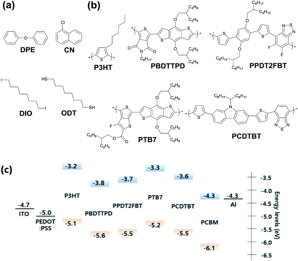 | ||
| Fig. 1 The molecular structure of the (a) processing additives and (b) donor polymers. (c) The energy band diagram of the components in the PSCs. | ||
We fabricated PSCs with a simple and conventional structure of ITO/PEDOT:PSS/polymer:PCBM/Al. Fig. 1c presents the energy band diagrams of the components of the PSCs. We have only focused on the effect of processing additives on the device performance of PSCs based on different donor polymers without any interlayers. CB was used as the main solvent for depositing the active layer via a spin-coating method. The detailed methods for device fabrication are described in the Methods section. Fig. 2a–e show the current density versus voltage (J–V) characteristics of the PSCs with different donor polymers and processing additives. The external quantum efficiency (EQE) curves of the corresponding PSCs are shown in Fig. 2f and S1.† Furthermore, the detailed photovoltaic parameters for all the PSCs are summarized in Table 1.
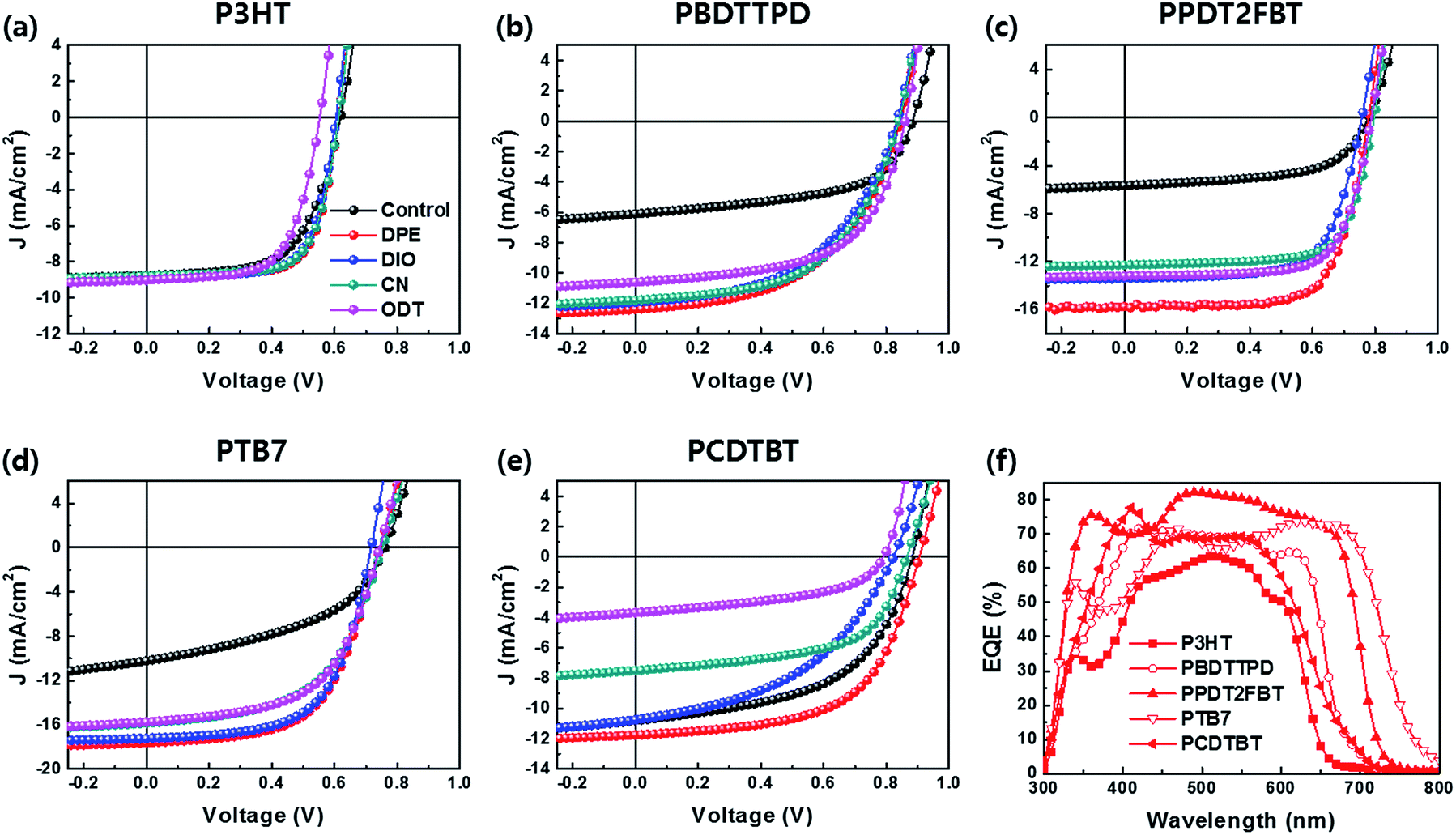 | ||
| Fig. 2 J–V characteristics of the BHJ PSCs based on (a) P3HT, (b) PBDTTPD, (c) PPDT2FBT, (d) PTB7, and (e) PCDTBT with different processing additives. (f) The EQE spectra of all the PSCs with DPE. | ||
| Polymer | Additives | JSC [mA cm−2] | VOC [V] | FF | PCE [%] |
|---|---|---|---|---|---|
| P3HT | Control | 8.76 | 0.62 | 0.61 | 3.29 |
| DPE | 8.85 | 0.61 | 0.70 | 3.77 | |
| DIO | 8.91 | 0.61 | 0.68 | 3.68 | |
| CN | 8.79 | 0.61 | 0.69 | 3.73 | |
| ODT | 9.02 | 0.55 | 0.64 | 3.18 | |
| PBDTTPD | Control | 6.10 | 0.88 | 0.55 | 2.98 |
| DPE | 12.4 | 0.85 | 0.52 | 5.40 | |
| DIO | 11.9 | 0.83 | 0.51 | 5.03 | |
| CN | 11.8 | 0.84 | 0.54 | 5.37 | |
| ODT | 10.6 | 0.86 | 0.58 | 5.32 | |
| PPDT2FBT | Control | 6.16 | 0.84 | 0.63 | 3.23 |
| DPE | 15.7 | 0.78 | 0.71 | 8.64 | |
| DIO | 13.4 | 0.76 | 0.68 | 6.84 | |
| CN | 12.3 | 0.80 | 0.71 | 6.97 | |
| ODT | 13.2 | 0.79 | 0.71 | 7.32 | |
| PTB7 | Control | 10.2 | 0.76 | 0.45 | 3.48 |
| DPE | 17.6 | 0.75 | 0.59 | 7.70 | |
| DIO | 17.2 | 0.72 | 0.61 | 7.55 | |
| CN | 15.9 | 0.75 | 0.55 | 6.57 | |
| ODT | 15.7 | 0.74 | 0.57 | 6.65 | |
| PCDTBT | Control | 10.8 | 0.88 | 0.53 | 5.07 |
| DPE | 11.7 | 0.91 | 0.59 | 6.27 | |
| DIO | 10.7 | 0.82 | 0.45 | 3.97 | |
| CN | 7.49 | 0.87 | 0.58 | 3.78 | |
| ODT | 3.68 | 0.79 | 0.48 | 1.38 |
There is no significant effect of the processing additives on the performance of the P3HT:PCBM PSCs. The control device without additive already showed a high PCE of 3.29% when compared to those of the devices with additives. However, the introduction of all the processing additives led to a slight increase in the fill factor (FF). Among the various processing additives studied, the device with DPE showed the highest FF value of 0.70 and a PCE of 3.77%. The devices with DIO and CN also achieved high device efficiencies of 3.68% and 3.73%, respectively. In contrast, the device with ODT showed a lower open-circuit voltage (VOC) of 0.55 V when compared to the other devices (0.61–0.62 V).
There are numerous differences in the device performance between the PBDTTPD-based devices with and without the processing additives. The device without additive exhibited a PCE of 2.98% with a short-circuit current density (JSC) of 6.10 mA cm−2, VOC of 0.88 V, and FF of 0.55. It is noticeable that all the devices with the additive showed high PCEs over 5% that are mostly attributed to remarkable increase in JSC (up to 12.41 mA cm−2). The same tendencies were observed in the PPDT2FBT and PTB7-based devices. The introduction of an additive has a great effect on the performance of the devices based on a semi-crystalline polymer (PPDT2FBT: 3.23% → 8.64% and PTB7: 3.48 → 7.70%). In particular, both the PPDT2FBT and PTB7 devices with DPE exhibited the highest JSC and PCE values among the devices with various processing additives. Compared to other donor polymers, a different tendency was observed in the device based on PCDTBT, which is known as one of the amorphous polymers used in PSCs. The control device without additive showed a PCE of 5.07%. Apart from the device with DPE, the other processing additives resulted in a significant decrease in the FF or JSC values. In contrast, DPE improved the device efficiency up to 6.27% due to a simultaneous increase in all the photovoltaic parameters.
Morphology characteristics
To understand the reason why DPE gives rise to the highest PCE among the various processing additives, we checked the solubility of the five donor polymers in each of the processing additives at 60 °C. As shown in Fig. 3, it is easily noticed that CN is a good solvent for all the polymers, whereas the other additives appear to act as a poor solvent. Interestingly, the colors of the polymer solutions dissolved in DPE were deeper than those of the solutions dissolved in DIO and ODT. This implies that DPE satisfies the theta condition at 60 °C, in which the solutions were stirred overnight to fabricate the active layers of PSCs, indicating that DPE can play a role as a theta solvent for all the polymers in poor solvents.37 In a theta solvent, the polymer coils act like ideal chains because the interaction between a theta solvent and a polymer is balanced at the theta point (the enthalpy of mixing is zero).38 Therefore, DPE can be widely used as a beneficial processing additive for BHJ PSCs regardless of the polymers crystallinity.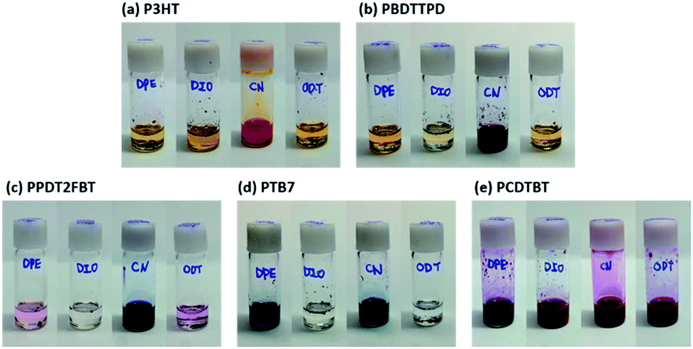 | ||
| Fig. 3 The solubility tests for five donor polymers in different processing additives (2.5 mg of polymer in 1 mL of solvent). | ||
The morphologies of the BHJ films with different processing additives were investigated via atomic force microscopy (AFM). The AFM topography images are shown in Fig. 4. The BHJ film based on P3HT without additive had a uniform surface with a low root-mean-square (RMS) roughness of 1.12 nm (Fig. 4a). The PCBM cannot aggregate freely in the intense interactions between the crystalline polymer chains, and therefore phase separation is difficult during solvent evaporation.39 After introducing the processing additives, small or large islands were observed, which may be attributed to the separation and growth of the PCBM molecules. Among the BHJ films with additives, the film with DPE exhibited the lowest RMS roughness of 4.89 nm (DIO: 6.74 nm, CN: 5.54 nm, and ODT: 7.53 nm).
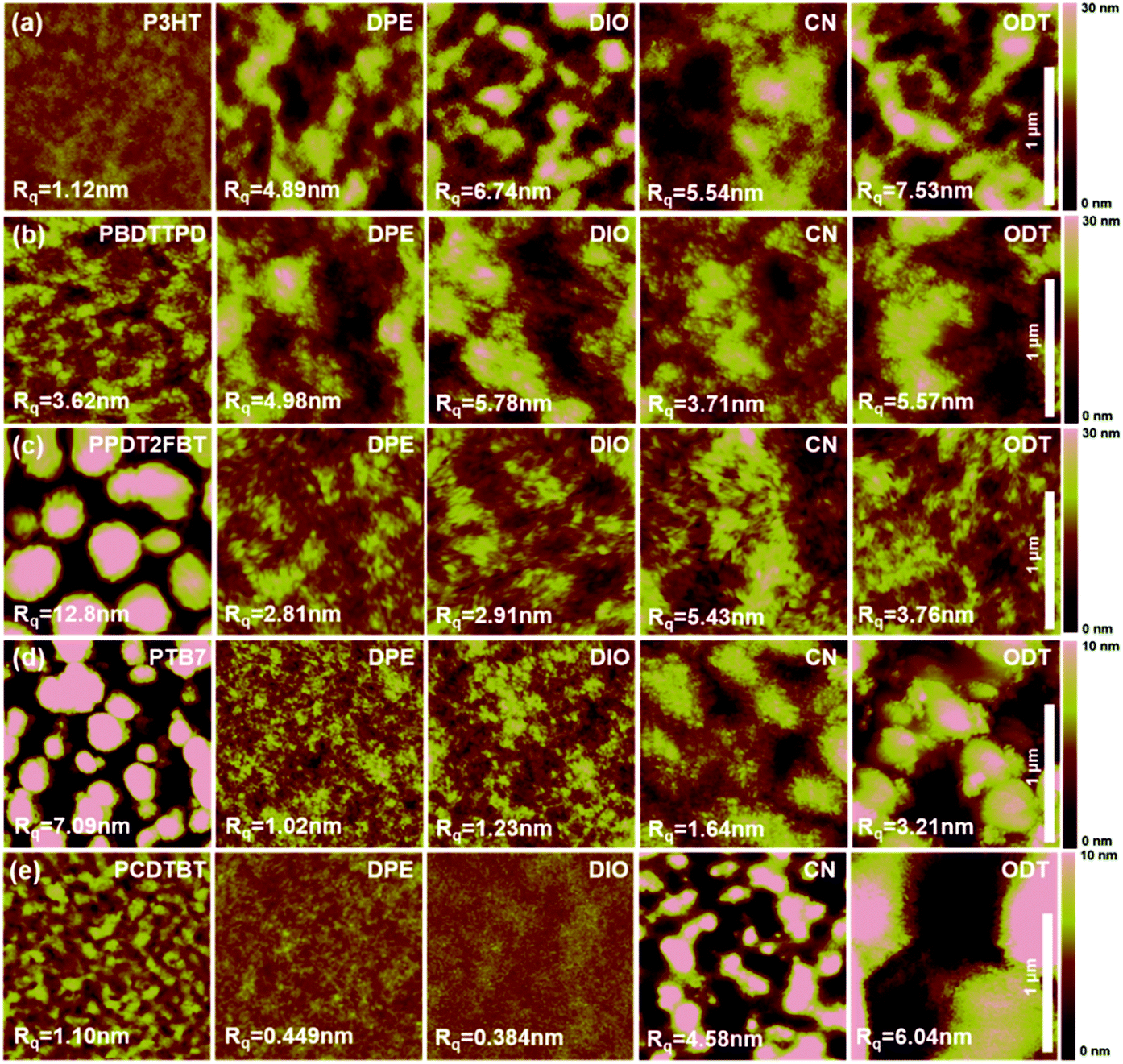 | ||
| Fig. 4 AFM topographical images of the (a) P3HT, (b) PBDTTPD, (c) PPDT2FBT, (d) PTB7, and (e) PCDTBT BHJ films without processing additives (1st column) and with DPE (2nd column), DIO (3rd column), CN (4th column), and ODT (5th column) deposited on ITO/PEDOT:PSS substrates. The root mean square values of the roughness for each film are given at the bottom-left corner of each image. | ||
Similar to P3HT, the introduction of a processing additive increased the surface roughness of the BHJ films based on PBDTTPD (Fig. 4b). Unlike the P3HT system, these rough surface morphologies remarkably enhanced the performance of the PBDTTPD:PC71BM devices. The film with CN had a lower roughness of 3.71 nm compared to that of the films containing the other additives (DPE: 4.98 nm, DIO: 5.78 nm and ODT: 5.57 nm). However, all the devices exhibited similar PCEs regardless of the additive used. We found that there is no correlation between surface roughness and device performance.
The morphologies of the BHJ film based on PPDT2FBT can be significantly modulated using the processing additive (Fig. 4c). The film without an additive showed an uneven surface with large domains (few hundreds of nanometers in diameter).5 This morphology led to poor device performance. In contrast, the introduction of the processing additives induced a uniform and smooth surface morphology. Among the additives, the smoothest surface roughness and nanofibrillar structure formed with DPE resulted in the highest device efficiency.
The morphologies of the BHJ films based on PTB7 were analogous to the PPDT2FBT system (Fig. 4d). The processing additives led to a uniform film with smooth surface roughness. However, the films prepared with CN and ODT exhibited larger agglomerations when compared to those with DPE and DIO. This differences gave rise to a distinction of the JSC. Specifically, a more even and smoother surface using DPE and DIO resulted in higher PCEs.
The PCDTBT:PC71BM BHJ films with DPE and DIO exhibited smooth surface roughness compared to that of the films with CN and ODT (without additive: 1.10 nm, DPE: 0.449 nm, DIO: 0.384 nm, CN: 4.58 nm and ODT: 6.04 nm) (Fig. 4e). The difference in the JSC value of the device based on PCDTBT can be attributed to morphological changes due to the different additives.
According to the AFM results obtained for various BHJ films, although a smooth and uniform surface induced by the introduction of an additive had a tendency to give rise to higher device performance, these morphologies did not guarantee the highest PCEs. Among the processing additives, however, the BHJ films with DPE have a low surface roughness (although not the lowest) and bicontinuous morphologies between polymer and PCBM, which could be the attributed to how DPE works as a theta solvent during the formation of the active layer film.
To investigate the changes in the molecular ordering and orientation in the BHJ films as a function of the processing additive, we measured the grazing incidence wide-angle X-ray scattering (GIWAXS). However, there are no significant changes in the polymer chain packing and intermolecular ordering when using different processing additives (Fig. S2†). This indicates that the processing additives play a role in changing the phase separation of the polymer and PCBM domain, but not the strength of intermolecular ordering or the direction of polymer chain packing. The line-cuts of the GIWAXS patterns and detailed crystallographic parameters are shown in Fig. S3 and Table S1.† The GIWAXS results do not support the effect of the different additives on the device performance.
Charge carrier recombination
The morphological changes in the BHJ films using different additives are deeply related to the degree of bimolecular recombination. The dependence of JSC on the light intensity can provide information on the bimolecular recombination occurring in the active layer.35,40 Therefore, we compared the JSC dependence with the light intensity (JSC vs. light intensity) of the devices as a function of the processing additive. The logarithmic plots of JSC vs. light intensity for each PSC are shown in Fig. 5. According to the power-law JSC dependence on the light intensity, the linear curves were fitted using eqn (1).| JSC ∝ Is | (1) |
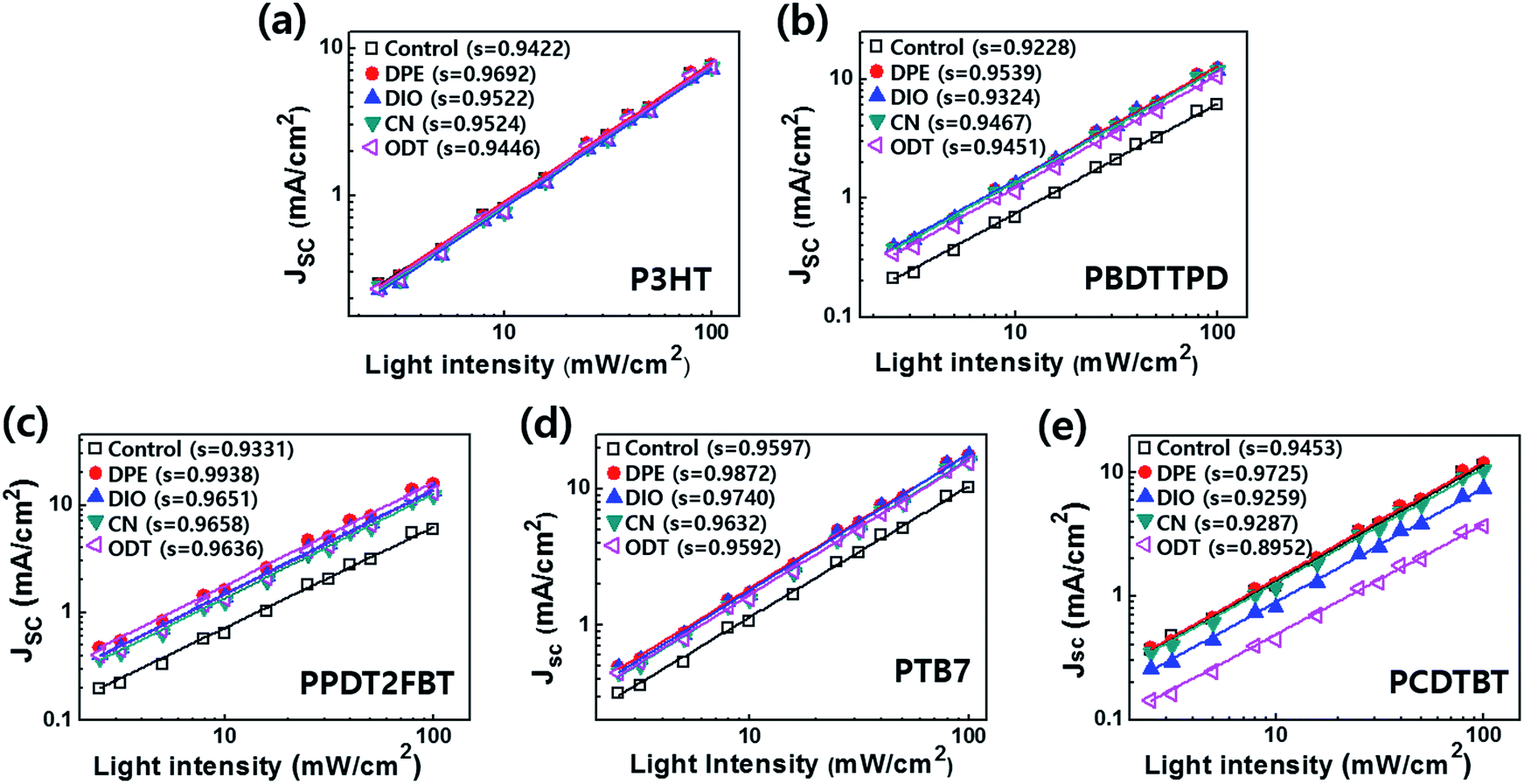 | ||
| Fig. 5 The JSC dependence on light intensity for the PSCs based on P3HT, PBDTTPD, PPDT2FBT, PTB7, and PCDTBT without processing additives (control) and with DPE, DIO, CN, and ODT. | ||
Conclusion
In conclusion, we successfully investigated the influence of various processing additives on the performance of devices based on five donor polymers with different crystallinity. The morphologies of the BHJ films based on the donor polymers with crystallinity are easily influenced by the processing additives. Although the morphological changes are not consistent with device performance, all the PSCs with DPE achieve the highest device efficiency regardless of the polymers crystallinity. These high PCEs are clearly attributed to the minimized bimolecular recombination within the active layer upon the introduction of DPE. In other words, DPE results in an ideal morphology in the BHJ system by acting as a theta solvent. This study can offer an effective way to control the morphology of the BHJ film and optimize the device performance using DPE in the BHJ PSCs regardless of the photovoltaic polymers used.Experimental
General
The AFM height and phase images were obtained using a Veeco AFM microscope in tapping mode. The light intensity dependence of the JSC value was measured with neutral density filters. GIWAXS measurements were carried out at the PLS-II 9A U-SAXS beam line of the Pohang Accelerator Laboratory.Fabrication and characterization of the PSCs
The device configuration of the PSCs was a conventional structure of glass/ITO/PEDOT:PSS/active layer/Al. Firstly, the patterned ITO coated glass substrates were cleaned in an ultrasonicator using deionized water, acetone, and isopropyl alcohol, and then, the substrates were dried in an oven at 100 °C overnight. The PEDOT:PSS (Baytron AI 4083) layer was spin coated on the substrate at 4000 rpm for 40 s, then baked on a hot plate at 140 °C for 10 minutes in the air. After baking, the substrates were moved into a glove box filled with nitrogen.
P3HT (number-average molecular weight (Mn) = 60 kDa, polydispersity index (PDI) = 1.4) was purchased from Organic Semiconductor Materials (OSM, Republic of Korea). PBDTTPD (weight-average molecular weight (Mw) = 39.5 kDa, PDI = 2.2), PTB7 (Mw = 10.8 kDa, PDI = 2.4), PCDTBT (Mw = 33 kDa, PDI = 2.3) were purchased from 1-Material. PPDT2FBT (Mn = 42.6 kDa, PDI = 2.8) was synthesized by us.5 The PSCs based on the five donor polymers were fabricated using different experimental conditions including solution concentration, D:A ratio and amount of the processing additive (DPE, DIO, CN and ODT). The solutions for P3HT:PC61BM (1:0.8, w/w), PPDT2FBT:PC71BM (1:1.5, w/w), PBDTTPD:PC71BM (1:1.5, w/w), PTB7:PC71BM (1:1.25, w/w) and PCDTBT:PC71BM (1:4, w/w) were dissolved in chlorobenzene (CB) with polymer concentrations of 13, 14, 8, 12 and 7 mg mL−1 with 2, 3, 5, 3 and 3 vol% of the additives, respectively. With the exception of PBDTTPD (110 °C), the other solutions were stirred at 60 °C overnight. After coating the active layer, the substrates were brought into a high vacuum chamber (∼10−6 Torr), and Al (100 nm) was deposited via a thermal evaporation process. In the case of the P3HT PSCs, after deposition of the Al layer, the devices were thermally annealed at 150 °C for 10 minutes to obtain an optimum device performance. The device area was 13 mm2. Measurements were conducted in a glove box using a high quality optical fiber to lead the light from a xenon arc lamp solar simulator. The J–V characteristics were measured under AM 1.5G illumination (100 mW cm−2) with a Keithley 2635A source measurement unit, and the EQE was measured in air using an EQE system (Model QEX7) via PV measurements Inc. (Boulder, Colorado).
Acknowledgements
This study was supported by the New & Renewable Energy Core Technology Program of the Korea Institute of Energy Technology Evaluation and Planning (KETEP), granted financial resource from the Ministry of Trade, Industry & Energy, Republic of Korea (20123010010140), the National Research Foundation of Korea (Grant No. NRF-2015R1C1A1A02036599, 2015M1A2A2057506) and Research Fund of Hanyang University (HY-2015).Notes and references
- J. Y. Kim, S. H. Kim, H. H. Lee, K. Lee, W. Ma, X. Gong and A. J. Heeger, Adv. Mater., 2006, 18, 572 CrossRef CAS.
- J. Y. Kim, K. Lee, N. E. Coates, D. Moses, T. Q. Nguyen, M. Dante and A. J. Heeger, Science, 2007, 317, 222 CrossRef CAS PubMed.
- J. Peet, J. Y. Kim, N. E. Coates, W. L. Ma, D. Moses, A. J. Heeger and G. C. Bazan, Nat. Mater., 2007, 6, 497 CrossRef CAS PubMed.
- Y. Liu, J. Zhao, Z. Li, C. Mu, W. Ma, H. Hu, K. Jiang, H. Lin, H. Ade and H. Yan, Nat. Commun., 2014, 5, 5293 CrossRef CAS PubMed.
- T. L. Nguyen, H. Choi, S. J. Ko, M. A. Uddin, B. Walker, S. Yum, J. E. Jeong, M. H. Yun, T. J. Shin, S. Hwang, J. Y. Kim and H. Y. Woo, Energy Environ. Sci., 2014, 7, 3040 CAS.
- Y. Li, T. H. Lee, S. Y. Park, M. A. Uddin, T. Kim, S. Hwang, J. Y. Kim and H. Y. Woo, Polym. Chem., 2016, 7, 4638 RSC.
- Y. Wang, H. Zhu, Z. Shi, F. Wang, B. Zhang, S. Dai and Z. a. Tan, J. Mater. Chem. A, 2016 10.1039/c6ta10678a.
- L. Yu, C. Li, Q. Li, F. Wang, J. Lin, J. Liu, S. Hu, H. Zheng and Z. a. Tan, Org. Electron., 2015, 23, 99–104 CrossRef CAS.
- X. Guo, C. Cui, M. Zhang, L. Huo, Y. Huang, J. Hou and Y. Li, Energy Environ. Sci., 2012, 5, 7943 CAS.
- T. Liu, L. Huo, X. Sun, B. Fan, Y. Cai, T. Kim, J. Y. Kim, H. Choi and Y. Sun, Adv. Energy Mater., 2016, 6, 1502109 CrossRef.
- L. Lu, W. Chen, T. Xu and L. Yu, Nat. Commun., 2015, 6, 7327 CrossRef CAS PubMed.
- L. Lu, M. A. Kelly, W. You and L. Yu, Nat. Photonics, 2015, 9, 491 CrossRef CAS.
- T. H. Lee, M. A. Uddin, C. Zhong, S.-J. Ko, B. Walker, T. Kim, Y. J. Yoon, S. Y. Park, A. J. Heeger, H. Y. Woo and J. Y. Kim, Adv. Energy Mater., 2016, 6, 1600637 CrossRef.
- H. Choi, J. Lee, W. Lee, S.-J. Ko, R. Yang, J. C. Lee, H. Y. Woo, C. Yang and J. Y. Kim, Org. Electron., 2013, 14, 3138 CrossRef CAS.
- T. Yang, M. Wang, C. Duan, X. Hu, L. Huang, J. Peng, F. Huang and X. Gong, Energy Environ. Sci., 2012, 5, 8208 CAS.
- H.-L. Yip and A. K. Y. Jen, Energy Environ. Sci., 2012, 5, 5994 CAS.
- A. R. b. M. Yusoff, D. Kim, H. P. Kim, F. K. Shneider, W. J. da Silva and J. Jang, Energy Environ. Sci., 2015, 8, 303 CAS.
- J. Zhang, Y. Zhang, J. Fang, K. Lu, Z. Wang, W. Ma and Z. Wei, J. Am. Chem. Soc., 2015, 137, 8176 CrossRef CAS PubMed.
- T. Erb, U. Zhokhavets, G. Gobsch, S. Raleva, B. Stühn, P. Schilinsky, C. Waldauf and C. J. Brabec, Adv. Funct. Mater., 2005, 15, 1193 CrossRef CAS.
- G. Li, V. Shrotriya, Y. Yao and Y. Yang, J. Appl. Phys., 2005, 98, 043704 CrossRef.
- G. Li, Y. Yao, H. Yang, V. Shrotriya, G. Yang and Y. Yang, Adv. Funct. Mater., 2007, 17, 1636 CrossRef CAS.
- E. Verploegen, C. E. Miller, K. Schmidt, Z. Bao and M. F. Toney, Chem. Mater., 2012, 24, 3923 CrossRef CAS.
- S. Chambon, R. Mens, K. Vandewal, E. Clodic, M. Scharber, L. Lutsen, J. Gelan, J. Manca, D. Vanderzande and P. Adriaensens, Sol. Energy Mater. Sol. Cells, 2012, 96, 210 CrossRef CAS.
- C.-Y. Lee, B. Kim, K. H. Kim, Y. Yoon, M. W. Lee, D. H. Choi, M. J. Ko, H. Kim, D.-K. Lee and K. Kim, Synth. Met., 2013, 164, 64 CrossRef CAS.
- K. H. Park, Y. J. Kim, G. B. Lee, T. K. An, C. E. Park, S.-K. Kwon and Y.-H. Kim, Adv. Funct. Mater., 2015, 25, 3991 CrossRef CAS.
- Y. Kim, J. Hong, J. H. Oh and C. Yang, Chem. Mater., 2013, 25, 3251 CrossRef CAS.
- Y. Kim, H. R. Yeom, J. Y. Kim and C. Yang, Energy Environ. Sci., 2013, 6, 1909 CAS.
- S. Kwon, J. K. Park, J. Kim, G. Kim, K. Yu, J. Lee, Y.-R. Jo, B.-J. Kim, H. Kang, J. Kim, H. Kim and K. Lee, J. Mater. Chem. A, 2015, 3, 7719 CAS.
- C. Yi, X. Hu, H. C. Liu, R. Hu, C.-H. Hsu, J. Zheng and X. Gong, J. Mater. Chem. C, 2015, 3, 26 RSC.
- Z. He, B. Xiao, F. Liu, H. Wu, Y. Yang, S. Xiao, C. Wang, T. P. Russell and Y. Cao, Nat. Photonics, 2015, 9, 174 CrossRef CAS.
- C. H. Y. Ho, Q. Dong, H. Yin, W. W. K. Leung, Q. Yang, H. K. H. Lee, S. W. Tsang and S. K. So, Adv. Mater. Interfaces, 2015, 2, 1500166 CrossRef.
- S. J. Lou, J. M. Szarko, T. Xu, L. Yu, T. J. Marks and L. X. Chen, J. Am. Chem. Soc., 2011, 133, 20661 CrossRef CAS PubMed.
- X. Ouyang, R. Peng, L. Ai, X. Zhang and Z. Ge, Nat. Photonics, 2015, 9, 520 CrossRef CAS.
- H. Choi, S.-J. Ko, T. Kim, P.-O. Morin, B. Walker, B. H. Lee, M. Leclerc, J. Y. Kim and A. J. Heeger, Adv. Mater., 2015, 27, 3318 CrossRef CAS PubMed.
- M. A. Uddin, T. H. Lee, S. Xu, S. Y. Park, T. Kim, S. Song, T. L. Nguyen, S.-j. Ko, S. Hwang, J. Y. Kim and H. Y. Woo, Chem. Mater., 2015, 27, 5997 CrossRef CAS.
- D. Liu, Z. Wang, S. Zhang, Z. Zheng, B. Yang, W. Ma and J. Hou, RSC Adv., 2015, 5, 69567 RSC.
- A. Raegen, M. Chowdhury, C. Calers, A. Schmatulla, U. Steiner and G. Reiter, Phys. Rev. Lett., 2010, 105, 227801 CrossRef PubMed.
- F. Brochard and P. G. Degennes, Macromolecules, 1977, 10, 1157–1161 CrossRef CAS.
- H. Zhang, H. Yao, W. Zhao, L. Ye and J. Hou, Adv. Energy Mater., 2016, 6, 1502177 CrossRef.
- L. J. A. Koster, V. D. Mihailetchi, H. Xie and P. W. M. Blom, Appl. Phys. Lett., 2005, 87, 203502 CrossRef.
Footnotes |
| † Electronic supplementary information (ESI) available: EQE spectra of devices and GIWAXS data can be found. See DOI: 10.1039/c6ra27944a |
| ‡ These authors contributed equally. |
| This journal is © The Royal Society of Chemistry 2017 |