
 Open Access Article
 This Open Access Article is licensed under a
 Creative Commons Attribution 3.0 Unported Licence
Physisorbed versus chemisorbed oxygen effect on thermoelectric properties of highly organized single walled carbon nanotube nanofilms†
Milad Yarali a,
Ji Haob,
Mohammad Khodadadia,
Hatem Brahmia,
Shuo Chencd,
Viktor G. Hadjievd,
Yung Joon Jungb and
Anastassios Mavrokefalos*a
a,
Ji Haob,
Mohammad Khodadadia,
Hatem Brahmia,
Shuo Chencd,
Viktor G. Hadjievd,
Yung Joon Jungb and
Anastassios Mavrokefalos*a
aDepartment of Mechanical Engineering, University of Houston, Houston, TX 77204, USA. E-mail: amavrokefalos@uh.edu; Tel: +1 713 743 4531
bDepartment of Mechanical and Industrial Engineering, Northeastern University, Boston, MA 02115, USA
cDepartment of Physics, University of Houston, Houston, TX 77204, USA
dTexas Center for Superconductivity at the University of Houston (TcSUH), Houston, TX 77204, USA
First published on 2nd March 2017
Abstract
The effect of physisorbed vs. chemisorbed oxygen on highly organized single walled carbon nanotube (SWCNT) ultrathin films is investigated by correlating the thermoelectric properties measured by a suspended micro-device to the SWCNT structure characterized by Raman spectroscopy and transmission electron microscopy. The results show that SWCNTs with weakly bonded oxygen molecules on the surface were determined to be initially p-type with metallic behavior and after annealing in vacuum they transition to n-type with semiconducting behavior where the charge transport is dominated by a 2D Mott variable range hopping mechanism due to molecular desorption. The structural characterization reveals that there is no change in the structure of the SWCNT network, indicating that the source of the drastic change in electrical properties is due to the molecule interaction with the surface of the SWCNT. Even though there is a significant change in the electrical properties, the thermal conductivity remains unchanged. On the other hand, the oxidized SWCNT sample with stronger C–O bonds exhibits purely p-type metallic behavior that is insensitive to annealing conditions and shows lower thermal conductivity values because of the enhanced phonon scattering due to the absorbed oxygen molecules and residual poly-methyl-methacrylate (PMMA).
1. Introduction
The importance of single walled carbon nanotube (SWCNT) networks in electronic and thermal applications cannot be understated. Recently, designing engineered carbon nanotube architectures composed of aligned nanotubes (horizontal or vertical) has attracted considerable interest due to broad applications in flexible electronic,1,2 optoelectronic,3 field emission4 and energy storage devices.5 The performance of these architectures is highly dependent on the exact structure of the individual nanotubes, their interactions within the network as well as their chemical interactions with the surrounding environment.6 To more efficiently design the next generation of micro–macroscopic functional devices, clarifying the thermoelectric properties such as thermal conductivity (κ), electrical conductivity (σ), and Seebeck coefficient (S) of these aligned CNT network is crucial.Over the last two decades, a great number of investigations have been conducted in studying various thermal and electrical properties of individual single-walled carbon nanotubes,7–16 multi-walled carbon nanotubes (MWCNTs),17–19 nanotube composites,20–24 and films.25–32 These studies are essential in quantifying the various external or intrinsic effects on the individual phonon or charge transport properties of these seminal materials. To understand their interdependence, on the other hand, it is essential to perform multiple property measurements on the same samples. Specifically by performing simultaneous measurement of thermoelectric properties such as thermal conductivity, electrical conductivity and Seebeck coefficient on the same sample, allows us to quantify both the phonon and electron transport properties as well as their interdependence not otherwise possible by single property measurements.33,34 Even though these types of measurements were performed on individual single- and multi-walled carbon nanotubes35,36 and supported bulk films with broader size distribution of randomly oriented and aligned arrays of SWCNTs and MWCNTs;37–41 measurements of thin and highly organized suspended films composed of SWCNT bundles, that can have a significant impact in a broad range of technologies as mentioned earlier are notably absent.
These thermoelectric properties of SWCNTs have shown to be extremely sensitive to their surrounding molecular environment, specifically oxygen, which can have detrimental effect to their intrinsic properties.31,32 Unfortunately, there are contradictory reports on the exact effect of oxygen adsorption on the SWCNT properties. Some studies which were performed on the bulk films composed of randomly oriented SWCNTs showed that adsorbed oxygen molecules on the tubes surface dope the nanotubes positively due to charge transfer between carbon atoms and oxygen.31,32,40–42 They claimed that oxygen removal by high temperature annealing of SWCNTs under ultrahigh vacuum or inert gas likely leads to hole de-doping from SWCNT. In contrast to this view, it has also been proposed that oxygen does not induce hole doping in SWCNTs.43 Derycke et al.44,45 and Heinze et al.46 have argued that p-type to n-type transition in electronic character of SWCNT field effect transistor (CNTFET) by annealing is because of the barrier change at the metal–semiconductor contacts due to oxygen desorption. Therefore, further work is required to determine which process leads to the observed changes in the transport properties of SWCNTs.
Moreover, although most of the previous works just focus on the effect of physisorbed oxygen on electrical conductivity and Seebeck coefficient of thick (macroscopic) SWCNT mats or films, its effect to thermal transport is notably absent. To the best of our knowledge there are only two contradicting reports on the effect of oxygen adsorption of multi-walled CNTs (MWCNTs)39,47 and none investigating its effect on SWCNTs where we are reporting for the first time. Jin et al.39 showed an increase in the thermal conductivity with the desorption of oxygen for MWCNTs that they attributed to the decrease in the resistivity of the thermal junctions between the tubes, whereas Brown et al.47 showed an increase in the thermal conductance of MWCNTs with oxygen adsorption which they attributed to the deformation of C–C bonds that affects the phonon modes of nanotubes.
In this work, we investigate the effect of physisorbed vs. chemisorbed oxygen on thermoelectric properties of ultrathin films composed of highly organized SWCNT bundles by utilizing a suspended microdevice. This method allows us to measure the thermal conductivity, electrical conductivity and Seebeck coefficient based on a four-probe thermoelectric measurement procedure reported in details elsewhere that accounts for the thermal contact resistance between the sample and the device.48 Therefore, the properties presented here are the intrinsic sample properties without the uncertainties of electrical or thermal contact resistances. Through correlating the thermoelectric properties to the SWCNT structure characterized by Raman spectroscopy and Transmission Electron Microscopy (TEM) and by fitting the measured thermoelectric properties with a two-band model, we are able to quantify how the physisorbed vs. chemisorbed oxygen molecules adsorbed to the CNT surface affect the thermoelectric properties. The results show that desorption of the weakly bonded oxygen molecules on the surface of SWCNTs after vacuum annealing changes the electrical behavior from metallic p-type to semiconducting n-type while its thermal conductivity remains unchanged, contradictory with reports on MWCNTs. On the contrary, purely p-type metallic behavior and lower thermal conductivity values were observed for oxidized SWCNT network.
2. Experimental
2.1. Sample preparation
In order to design and build horizontally organized SWCNT network on SiO2/Si substrates, a template-guided fluidic assembly method was employed. First, a plasma treatment was used to enhance the hydrophilic nature of Si or SiO2 surface. Then a photoresist film, providing hydrophobic surface on the Si or SiO2 substrate was patterned using optical or electron-beam lithography techniques and vertically submerged into the SWNT solution using a dip-coater and then gradually lifted from the solution with a constant pulling speed. We used the SWCNT-DI (de-ionized) water dispersion (concentration of 0.23 wt%) that was purchased from Brewer Science Inc. (CNTRENETM C100). The nanotubes were CVD grown and of mixed chirality in nature. The typical length of the SWCNTs was specified to be between 0.8 μm and 1 μm, with an average diameter of about 1 nm. Our own AFM and Raman spectroscopy measurements were mostly in agreement with about ∼10% deviation in specified length range and diameter. According to the vendor, the SWCNTs were not purified, and the dispersion was a mixture containing a natural ratio of metallic and semiconducting nanotubes, which can be assumed to be approximately 2/3rd semiconducting and 1/3rd metallic in nature. These SWCNTs were terminated with carboxylic acid groups, which adsorb ions such as H+ and OH− from the aqueous solution leading to the presence of a net charge on the surface of SWCNTs. Using such a lithographically patterned template assisted dip-coating method, SWCNTs were directly assembled on hydrophilic surface, between pre-designed photoresist channels, forming organized SWCNT lateral networks in diverse geometries with feature sizes ranging from 100 nm to few microns.492.2. Device fabrication
The suspended microdevice used to perform the in situ measurements is illustrated in Fig. 1(a). The device incorporates two adjacent silicon nitride (SiNx) membranes suspended by six SiNx beams over a through-substrate hole. Two platinum (Pt) electrodes are patterned on each membrane to measure the electrical conductivity in a four-probe configuration and eliminate the contact electrical resistance. A serpentine Pt resistance thermometer is patterned on each membrane for measuring the thermal conductivity and Seebeck coefficient based on a four-probe thermoelectric measurement procedure. The through-substrate hole under the two membranes allowed us to conduct TEM measurement of the SWCNT network assembled on the suspended device.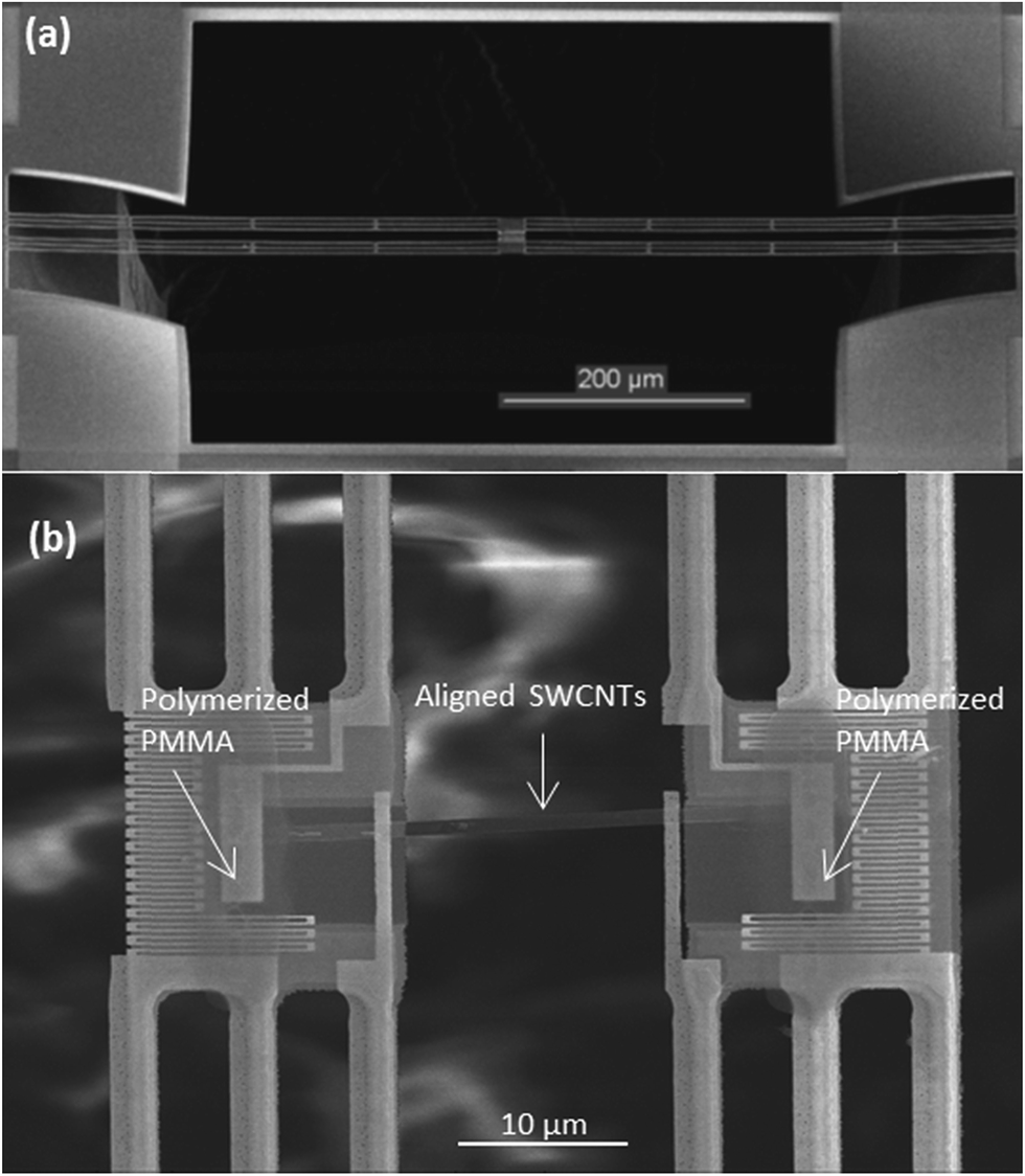 | ||
| Fig. 1 (a) SEM image of the suspended microdevice, (b) SEM close-up of aligned SWCNT network assembled between the membranes. PMMA polymerization area is pointed on each membrane. | ||
2.3. Measurement procedure
The widely used poly(methyl methacrylate) (PMMA)-assisted transfer technique50 was used to transfer horizontally organized SWCNTs onto a suspended measurement microdevice. To enhance the adhesion between samples and the membranes, a defined area of PMMA located on each membrane was polymerized, as shown in the Fig. 1(b). This was done by exposing a small concentrated area of the PMMA to 15 kV electron beam for 1 minute in a scanning electron microscope (SEM). This polymerization allowed us to anchor the samples on the membranes and guaranteed their attachment during PMMA removal by hot acetone.A total of two highly organized SWCNT nanofilms are reported in this work, denoted as sample 1 and sample 2. The thermal conductance and Seebeck coefficient measurements were conducted on the samples in a vacuum-pumped cryostat according to the previously described procedure.33,48,51–53 Both samples were in contact with all four Pt electrodes on the two suspended membranes. The four-probe electrical resistance of the samples was measured by using the two outer Pt electrodes as current leads and the two inner Pt electrodes to measure the voltage drop.
Sample 1 was previously air saturated under ambient conditions for several days and then the measurement was conducted for a temperature range of 300–425 K ascending in temperature every 25 K (heating path). We then kept the sample at 425 K in vacuum (10−7 mbar) overnight and performed the measurements again starting from 400 K to 300 K descending in temperature every 25 K (cooling path). Sample 2 was annealed in air at 350 °C for 3 hours before conducting the measurements from 300–425 K. As discussed later we also annealed the sample in vacuum (10−7 mbar) overnight to try and reproduce similar results as in sample 1. Both samples were kept at each temperature for 3 to 4 hours to reach steady state condition and then 3 sets of Seebeck coefficient data, each of which took approximately 15 minutes, were taken for each temperature consecutively.
Upon completion of thermoelectric measurements, the samples were removed from the cryostat and then TEM and Raman spectroscopy were performed to correlate the properties to structure. Dimensions of the suspended segment of the samples were measured using SEM and atomic force microscopy (AFM) (see Fig. S1 in the ESI†) and tabulated in Table 1. These dimensions were used to calculate the thermal conductivity and electrical conductivity from the measured thermal conductance and electrical resistance.
| Sample | Suspended length (μm) | Width (μm) | Thickness (nm) |
|---|---|---|---|
| 1 | 15.21 ± 0.08 | 1.05 ± 0.099 | 19 ± 2.48 |
| 2 | 7.97 ± 0.052 | 0.95 ± 0.074 | 19 ± 2.48 |
3. Results and discussion
3.1. Structural characterization
TEM and SEM images of sample 1 are shown in Fig. 2(a). No significant PMMA residues were observed on the film and the structure of this sample remains unchanged upon PMMA transferring and thermoelectric characterization. This is also verified by Raman spectroscopy characterization shown in Fig. S3 (see ESI† for more details). Sample 2 on the other hand shows some sample deformation as well as the presence of PMMA residues on the surface as seen in Fig. 2(b). Unfortunately thermal annealing in air was found to be ineffective to burn out these residues. Similar polymer residue was observed on the surface of suspended graphene or h-BN samples that were in contact with a PMMA layer during sample preparation.54–56 The effect of this unwanted polymer residues on the thermoelectric properties of this sample will be discussed later.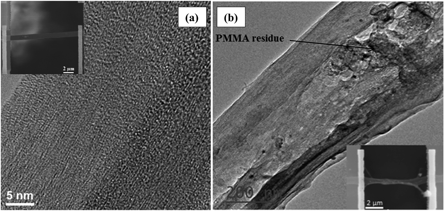 | ||
| Fig. 2 TEM and SEM images of (a) samples 1 and (b) sample 2. The PMMA residue is pointed out by arrow. | ||
To fully characterize the sample structures beyond TEM, we carried out Raman spectroscopy characterization of both samples after thermoelectric characterization. The Raman spectra allow us to obtain the SWCNTs diameter distribution,57 electronic type (semiconducting or metallic),58 appearance of oxidation induced defects,59 and the degree of nanotube alignment along the longest side of a ribbon. Fig. 3(a) shows the Raman spectra of radial breathing mode (RBM) in the nanofilms excited with three different laser lines. The RBM is a characteristic phonon mode of a nanotube in which all atoms vibrate in radial direction. The RBM phonon frequency ωRBM ∝ 1/d and the resonant optical transition energies Eii determines uniquely the nanotube diameter d and its electronic type.57,58 The RBM of semiconducting and metallic nanotubes in Fig. 3(a) are denoted by Sii and Mii, respectively, when the laser energy is close to Eii. For the given diameter distribution in sample 1, the laser line at 514 nm excites predominantly semiconducting SWCNTs whereas that at 633 nm mostly the metallic ones. The weaker RBM spectra of sample 2 excited with 633 nm line is due to smearing of the resonances by increased number of defects. The latter is also confirmed by the D- and G-mode Raman spectra shown in Fig. 3(b). The spectra of metallic nanotubes excited with 633 nm exhibit strong increase of the “defect” D-band. On the other hand, the oxidation of the semiconducting nanotubes, seen under 514 nm excitation, results in their protonation, p-type doping, with associated nanotube shrinkage and the corresponding increase of G-mode frequency.59
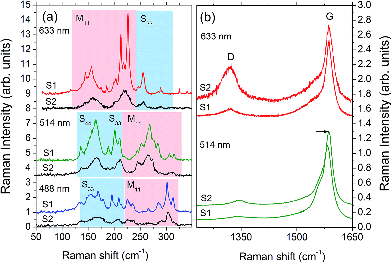 | ||
| Fig. 3 (a) Raman spectra of radial breathing modes in samples 1 (S1) and 2 (S2) excited with three different laser lines. Frequency ranges of metallic (M11) and semiconducting (S33 and S44) SWCNT are shaded in pink and blue, respectively. (b) Raman spectra of D and G modes in S1 and S2 (oxidized SWCNT). Note the upward shift of the G mode in S2 when excited with 514 nm laser. | ||
The alignment of SWCNTs along the longest side R of nanofilm ribbons was quantitatively determined by measuring the variation of G-mode Raman intensity IVV of SWNTs with angle Ψ between the R direction and the polarization direction of incident light as shown in Fig. 4. The inset in Fig. 4 displays a schematic diagram of the Raman configuration for measurement of angular dependence of the G mode intensity in back scattering configuration and for parallel incident, eI, and scattered, eS, light polarizations. In this experiment, the sample was rotated at angle Ψ while keeping the parallel incident and scattered light polarization directions fixed. The deviation angle of SWCNTs with respect to R is denoted by θ. The line through the data for the IVV(Ψ)/IVV(0) plot presents a fit to the function IVV = A + B![[thin space (1/6-em)]](https://www.rsc.org/images/entities/char_2009.gif) cos2Ψ + Ccos4Ψ. The correspondence between fitting parameters A, B, and C and orientation order parameters P2(cosθ) and P4(cosθ) is given by the expression:60
cos2Ψ + Ccos4Ψ. The correspondence between fitting parameters A, B, and C and orientation order parameters P2(cosθ) and P4(cosθ) is given by the expression:60
 θ) and P4(cosθ) are the average values of second- and fourth-order Legendre polynomials, respectively, over θ from 0 to π. The orientation order parameter P2(cosθ) (also known as the Herman's orientation function) is a measure of the mean orientation angle, whereas P4(cosθ) is needed for a reconstruction of the orientation distribution function. SWCNTs in the sample 1 are relatively well aligned along R having P2(cosθ) = 0.87 and P4(cosθ) = 0.48, perfectly aligned SWCNTs are characterized by P2(cosθ) = 1, whereas for randomly oriented ones P2(cosθ) = 0.
 | ||
| Fig. 4 Angular dependence of G mode intensity IVV in sample 1. Intensities are obtained by deconvolution of the baseline corrected spectra using mixed Gaussian and Lorentzian functions. The line through the data for the IVV vs. Ψ plot corresponds to a fit to the function IVV = A + Bcos2Ψ + Ccos4Ψ. Schematic diagram: eI and eS are the direction of incident and scattered light polarizations, R – direction of longest side of sample 1 ribbon, θ – angular deviation of SWCNTs from R. | ||
3.2. Thermoelectric properties
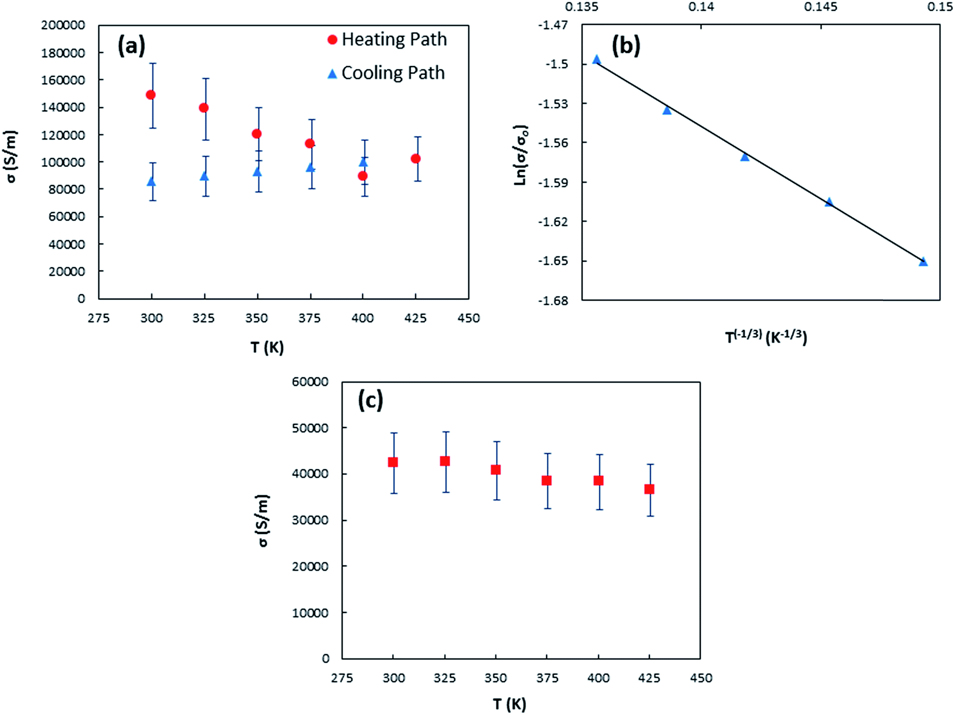 | ||
| Fig. 5 (a) Temperature dependent electrical conductivity of sample 1 for both heating and cooling paths (b) fitting of sample 1-cooling path electrical conductivity with eqn (1) (c) temperature dependent electrical conductivity of sample 2. | ||
Mott VRH model describes a system which is strongly disordered with the charge carriers hopping between localized states.69 The VRH relationship between conductance and temperature is given by:68
 | (1) |
Metallic behavior in electrical conductivity as depicted in Fig. 5(c) was observed for sample 2 because of oxidization by annealing in air environment. Also, sample 2 possesses smaller electrical conductivity when compared to sample 1 due to disruption of the π-bonded conduction path at either preexisting or newly created defect sites on the tubes during annealing process78,79 and the observed PMMA residue on the oxidized sample that affects the carrier mobility as it was well studied for graphene field-effect transistors (GFETs) by Suk et al.80 They observed experimentally that higher PMMA residue on transferred graphene samples results lower carrier mobility and can hence attribute to reduce electrical conductivity significantly.
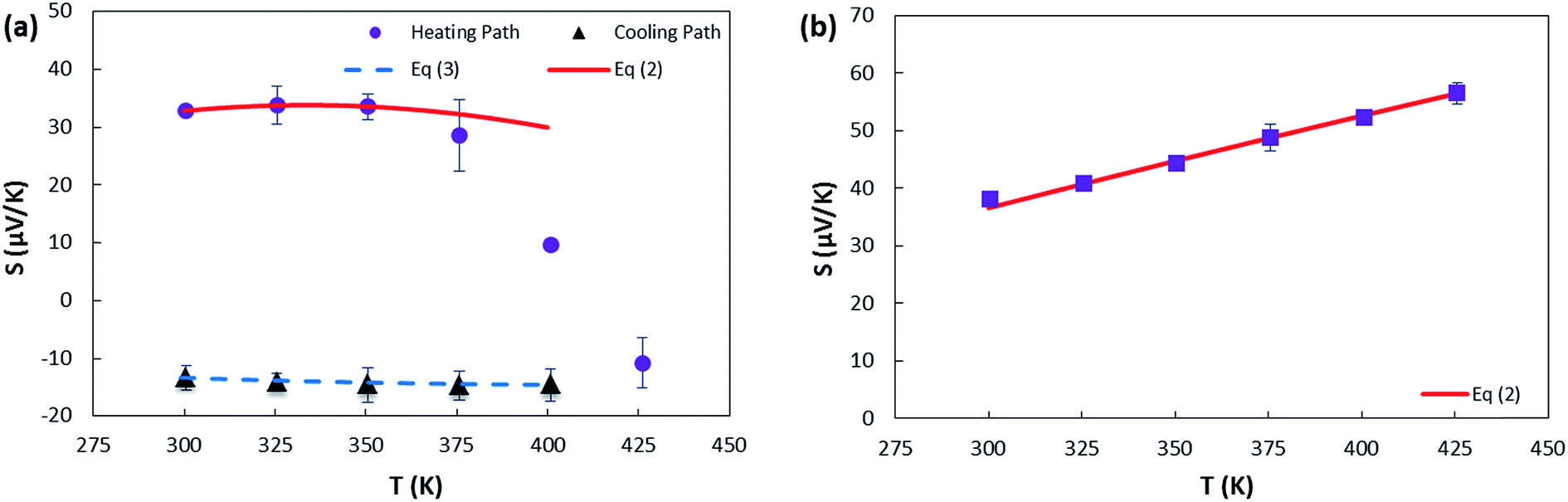 | ||
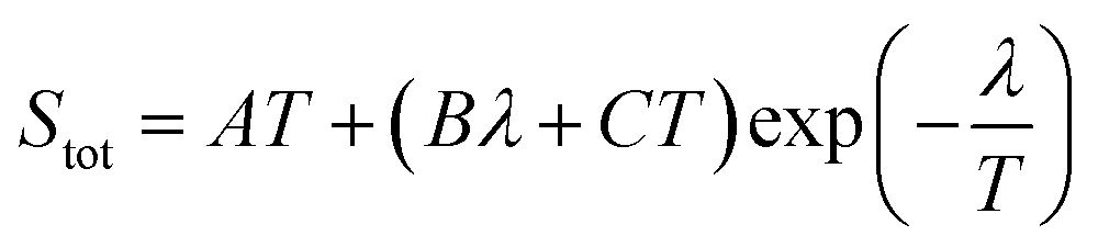
| Fig. 6 The variation of Seebeck coefficient versus temperature for (a) sample 1. The solid and dashed lines represent fits to the data using eqn (2) and (3), respectively. The fitting parameters extracted from the fit of heating path to eqn (2) are A = 0.030 μV K−2; B = 0.77 μV K−2; C = −0.95 μV K−2; λ = 600 K. The fitting parameters extracted from the fit of cooling path to eqn (3) are A = 0.16 μV K−2; B = −47.46 μV K−(4/3); T0 = 1351.8 K; d = 2 (the values of T0 and d are determined from electrical conductivity data) (b) sample 2. The fitting parameters extracted from the fit of heating path to eqn (2) are A = 0.04 μV K−2; B = 0.19 μV K−2; C = 0.06 μV K−2; λ = 400 K. | ||
As depicted in Fig. 6(b) sample 2 has large and positive Seebeck coefficient that increases with temperature as described in detail below. Annealing the sample overnight did not reproduce the sign change that occurred in sample 1. According to Fig. 2(b), PMMA residues are observed on sample 2 that can cause weak p-doping as it was reported previously for graphene.80,81 However, these residues cannot prevent the transition from p-type to n-type upon high temperature vacuum annealing as it was found that a p-CNTFET protected by PMMA can be converted into an n-FET by annealing in a vacuum at 200 °C which is not stable under ambient air pressure.45 This implies that annealing the sample in air, the oxygen molecules are chemisorbed on the SWCNT surfaces and PMMA residues, oxidizing thus this sample, and results in a larger density of holes due to a greater number of strongly bound oxygen acceptors. This makes the SWCNT network permanently p-type so that even when vacuum annealing was applied, we were unable to change the S sign.
 | (2) |
 | (3) |
 | ||
| Fig. 7 (a) Thermal conductivity versus temperature for (a) sample 1 and (b) sample 2. | ||
Our measured room temperature thermal conductivity of sample 1 is well matched with previously reported data in ref. 6 for the same highly organized SWCNT nanofilm and >3 times greater than the recently reported thermal conductivity of randomly oriented and nanometer thick supported87 and suspended88 SWCNT films. It is known that the thermal conductivity is dominated by phonons rather than electrons in the CNT networks throughout the whole temperature range.39,89,90 Since the maximum thermal conductivity occurs along the axis of CNT, fabricating CNT arrays in the aligned fashion could reduce the contact barriers and phonon scattering as a result. As shown in Fig. 7(a) the thermal conductivity of sample 1 remains unchanged after deoxygenating. This is contradictory with the report by Jin et al.39 which has showed that for MWCNTs annealed in inert environment at 100 °C for 4 hours (comparable with our annealing conditions), a 3-fold enhancement in thermal conductivity at 300 K compared to the as grown samples, indicating that oxygen desorption increases thermal conductivity through reducing the resistivity of the thermal junctions between the tubes. It is also contradictory with the report by Brown et al.47 that showed physisorbed oxygen molecules enhance the thermal conductance of MWCNTs bundles by 20% due to deformation of C–C bonds that affects the phonon modes of nanotubes as well as facilitating the inter-shell transfer of heat in the nanotubes. From our work, it can be concluded thus that the physisorbed oxygen molecules have negligible effect on the phonon transport in such ultrathin SWCNT film. However, for the chemisorbed sample we see a different trend, Fig. 7(b) depicts smaller thermal conductivity for sample 2 compared to that of sample 1 for the whole temperature range. The main factors responsible for providing phonon scattering sites and thereby the significant reduction in thermal conductivity of sample 2 are: 1 – chemisorbs oxygen molecules due to annealing in air that increase the C–O bonds especially in the defect sites or open ends of CNTs and 2 – the presence of PMMA residue that was observed on suspended segment of this sample. The influence of latter one on scattering of phonons in suspended bilayer graphene was reported by Pettes et al.91 In addition, the thermal conductivity of sample 2 was observed to be monotonically increasing with the temperature in the range studied. It was investigated computationally that introduced defects on SWCNTs may affect the phonon dispersion relation and therefore the temperature at which the thermal conductivity peak occurs can be influenced.92 The mechanism of thermal conduction is more complicated for a SWCNT thin film with existence of impurities, as in the present sample.
4. Conclusions
This study presents in situ measurement of thermal and electrical conductivity and Seebeck coefficient of highly organized SWCNT nanofilms. Fluidic assembly method was employed to produce horizontally aligned SWCNT films with average thickness of 19 nm. The results show that the SWCNT nanofilm with physisorbed oxygen molecules exhibits p-type with metallic behavior in electrical conductivity. Vacuum annealing leads to desorption of the oxygen molecule that transitions the nanofilms to n-type with semiconducting behavior in electrical conductivity that can be fitted with 2D variable range hopping. However, the thermal conductivity remains unchanged after the vacuum annealing. Since four probe configuration was utilized to perform the measurements and structural characterization revealed no change in the SWCNT film structure, we believe that this remarkable change in the thermoelectric properties of SWCNT nanofilm is purely due to oxygen desorption. Moreover, annealing the SWCNT films in air causes the oxygen molecule to chemisorb on the SWCNT nanofilm surface and (a) transforms the SWCNT nanofilm permanently p-type with metallic behavior in electrical conductivity and (b) significantly reduces the thermal conductivity by enhancing phonon scattering due to increase in the impurity concentration.Acknowledgements
AM acknowledges financial support from University of Houston. Y. J. J. acknowledges the financial support from National Science Foundation-DMEREF (1434824) and Technology Innovation Program (10050481) funded by the Ministry of Trade, Industry & Energy, Korea. V. G. H work was supported by the State of Texas through the Texas Center for Superconductivity at the University of Houston (TcSUH).Notes and references
- E. Artukovic, M. Kaempgen, D. S. Hecht, S. Roth and G. Grüner, Nano Lett., 2005, 5, 757–760 CrossRef CAS PubMed.
- J.-H. Ahn, H.-S. Kim, K. J. Lee, S. Jeon, S. J. Kang, Y. Sun, R. G. Nuzzo and J. A. Rogers, Science, 2006, 314, 1754–1757 CrossRef CAS PubMed.
- Z. Wu, Z. Chen, X. Du, J. M. Logan, J. Sippel, M. Nikolou, K. Kamaras, J. R. Reynolds, D. B. Tanner, A. F. Hebard and A. G. Rinzler, Science, 2004, 305, 1273–1276 CrossRef CAS PubMed.
- Y. J. Jung, S. Kar, S. Talapatra, C. Soldano, G. Viswanathan, X. Li, Z. Yao, F. S. Ou, A. Avadhanula, R. Vajtai, S. Curran, O. Nalamasu and P. M. Ajayan, Nano Lett., 2006, 6, 413–418 CrossRef CAS PubMed.
- R. Warren, F. Sammoura, K. S. Teh, A. Kozinda, X. Zang and L. Lin, Sens. Actuators, A, 2015, 231, 65–73 CrossRef CAS.
- H. Y. Jung, P. T. Araujo, Y. L. Kim, S. M. Jung, X. Jia, S. Hong, C. W. Ahn, J. Kong, M. S. Dresselhaus, S. Kar and Y. J. Jung, Nat. Commun., 2014, 5, 4941 CrossRef CAS PubMed.
- M. A. Osman and D. Srivastava, Nanotechnology, 2001, 12, 21–24 CrossRef CAS.
- S. Berber, Y. K. Kwon and D. Tománek, Phys. Rev. Lett., 2000, 84, 4613–4616 CrossRef CAS PubMed.
- E. Pop, D. Mann, Q. Wang, K. Goodson and H. Dai, Nano Lett., 2006, 6(1), 96–100 CrossRef CAS PubMed.
- J. R. Lukes and H. Zhong, J. Heat Transfer, 2007, 129(6), 705–716 CrossRef CAS.
- C. W. Padgett and D. W. Brenner, Nano Lett., 2004, 4(6), 1051–1053 CrossRef CAS.
- N. Mingo and D. A. Broido, Nano Lett., 2005, 5(7), 1221–1225 CrossRef CAS PubMed.
- N. Mingo and D. A. Broido, Phys. Rev. Lett., 2005, 95, 096105 CrossRef CAS PubMed.
- R. Pan, Z. Xu, Z. Zhu and Z. Wang, Nanotechnology, 2007, 18(28), 285704 CrossRef.
- C. Zhou, J. Kong and H. Dai, Phys. Rev. Lett., 2000, 84(24), 5604–5607 CrossRef CAS PubMed.
- A. Javey, M. Shim and H. Dai, Appl. Phys. Lett., 2002, 80(6), 1064–1066 CrossRef CAS.
- M. Fujii, X. Zhang, H. Xie, H. Ago, K. Takahashi, T. Ikuta, H. Abe and T. Shimizu, Phys. Rev. Lett., 2005, 95, 065502 CrossRef PubMed.
- L. Lu, N. Kang, W. J. Kong, D. L. Zhang, Z. W. Pan and S. S. Xie, Phys. E, 2003, 18, 214–215 CrossRef CAS.
- N. Kang, L. Lu, W. J. Kong, J. S. Hu, W. Yi, Y. P. Wang, D. L. Zhang, Z. W. Pan and S. S. Xie, Phys. Rev. B: Condens. Matter Mater. Phys., 2003, 67, 033404–033408 CrossRef.
- S. Shenogin, L. Xue, R. Ozisik, R. Keblinski and D. Cahill, J. Appl. Phys., 2004, 95, 8136–8144 CrossRef CAS.
- Q. Z. Xue, Nanotechnology, 2006, 17(6), 1655–1660 CrossRef CAS PubMed.
- S. U. S. Choi, Z. G. Zhang, W. Yu, F. E. Lockwood and E. A. Grulke, Appl. Phys. Lett., 2001, 79, 2252–2254 CrossRef CAS.
- M. J. Biercuk, M. C. Llaguno, M. Radosavljevic, J. K. Hyun, A. T. Johnsond and J. E. Fischer, Appl. Phys. Lett., 2002, 80, 2767–2769 CrossRef CAS.
- C. Guthy, F. Du, S. Brand, K. I. Winey and J. E. Fischer, J. Heat Transfer, 2007, 129(8), 1096–1099 CrossRef CAS.
- X. J. Hu, A. A. Padilla, J. Xu, T. S. Fisher and K. E. Goodson, J. Heat Transfer, 2006, 128(11), 1109–1113 CrossRef CAS.
- D. J. Yang, Q. Zhang, G. Chen, S. F. Yoon, J. Ahn, S. G. Wang, Q. Zhou, Q. Wang and J. Q. Li, Phys. Rev. B: Condens. Matter Mater. Phys., 2002, 66, 165440 CrossRef.
- T. Tong, Y. Zhao, L. Delzeit, A. Kashani, M. Meyyappan and A. Majumdar, IEEE Trans. Compon. Packag. Technol., 2007, 30(1), 92–100 CrossRef CAS.
- M. L. Bauer, Q. N. Pham, C. B. Saltonstall and P. M. Norris, Appl. Phys. Lett., 2014, 105, 151909 CrossRef.
- S. Shaikh, L. Li, K. Lafdi and J. Huie, Carbon, 2007, 45, 2608–2613 CrossRef CAS.
- M. A. Panzer, G. Zhang, D. Mann, X. Hu, E. Pop, H. Dai and K. E. Goodson, J. Heat Transfer, 2008, 130, 052401 CrossRef.
- K. Bradley, S. H. Jhi, P. G. Collins, J. Hone, M. L. Cohen, S. G. Louie and A. Zettl, Phys. Rev. Lett., 2000, 85(20), 4361–4364 CrossRef CAS PubMed.
- P. G. Collins, K. Bradley, I. Masa and A. Zettl, Science, 2000, 287, 1801–1804 CrossRef CAS PubMed.
- A. Mavrokefalos, A. L. Moore, M. T. Pettes, L. Shi, W. Wang and X. Li, J. Appl. Phys., 2009, 105, 104318 CrossRef.
- F. Zhou, J. Szczech, M. T. Pettes, A. L. Moore, S. Jin and L. Shi, Nano Lett., 2007, 7(6), 1649–1654 CrossRef CAS PubMed.
- C. Yu, L. Shi, Z. Yao, D. Li and A. Majumdar, Nano Lett., 2005, 5(9), 1842–1846 CrossRef CAS PubMed.
- P. Kim, L. Shi, A. Majumdar and P. L. McEuen, Phys. Rev. Lett., 2001, 87, 215502 CrossRef CAS PubMed.
- J. Hone, M. C. Llaguno, N. M. Nemes, A. T. Johnson, J. E. Fischer, D. A. Walters, M. J. Casavant, J. Schmidt and R. E. Smalley, Appl. Phys. Lett., 2000, 77, 666–668 CrossRef CAS.
- M. B. Jakubinek, M. A. White, G. Li, C. Jayasinghe, W. Cho, M. J. Schulz and V. Shanov, Carbon, 2010, 48, 3947–3952 CrossRef CAS.
- R. Jin, Z. X. Zhou, D. Mandrus, I. N. Ivanov, G. Eres, J. Y. Howe, A. A. Puretzky and D. B. Geohhegan, Phys. B, 2007, 388, 326–330 CrossRef CAS.
- H. E. Romero, G. U. Sumanasekera, G. D. Mahan and P. C. Eklund, Phys. Rev. B: Condens. Matter Mater. Phys., 2002, 65, 205410 CrossRef.
- G. U. Sumanasekera, C. K. W. Adu, S. Fang and P. C. Eklund, Phys. Rev. Lett., 2000, 85(5), 1096–1099 CrossRef CAS PubMed.
- X. Li, J. S. Huang, S. Nejati, L. McMillon, S. Huang, C. O. Osuji, N. Hazari and A. D. Taylor, Nano Lett., 2014, 14, 6179–6184 CrossRef CAS PubMed.
- H. Ulbricht, G. Moos and T. Hertel, Phys. Rev. B: Condens. Matter Mater. Phys., 2002, 66, 075404 CrossRef.
- V. Derycke, R. Martel, J. Appenzeller and P. H. Avouris, Appl. Phys. Lett., 2002, 80(15), 2773–2775 CrossRef CAS.
- V. Derycke, R. Martel, J. Appenzeller and P. H. Avouris, Nano Lett., 2001, 1, 453–456 CrossRef CAS.
- S. Heinze, J. Tersoff, R. Martel, V. Derycke, J. Appenzeller and P. H. Avouris, Phys. Rev. Lett., 2002, 89(10), 106801 CrossRef CAS PubMed.
- E. Brown, L. Hao, J. C. Gallop, J. C. Macfarlane, P. W. Josephs-Franks and L. F. Cohen, Phys. Status Solidi B, 2006, 243(13), 3380–3384 CrossRef CAS.
- A. Mavrokefalos, M. T. Pettes, F. Zhou and L. Shi, Rev. Sci. Instrum., 2007, 78, 034901 CrossRef PubMed.
- B. Li, M. G. Hahm, Y. L. Kim, H. Y. Jung, S. Kar and Y. J. Jung, ACS Nano, 2011, 5(6), 4826–4834 CrossRef CAS PubMed.
- G. B. Barin, Y. Song, I. D. F. Gimenez, A. G. S. Filho, L. S. Barreto and J. Kong, Carbon, 2015, 84, 82–90 CrossRef.
- L. Shi, D. Li, C. Yu, W. Jang, D. Kim, Z. Yao, P. Kim and A. Majumdar, J. Heat Transfer, 2003, 125, 881–888 CrossRef CAS.
- J. Zhou, C. Jin, J. H. Seol, X. Li and L. Shi, Appl. Phys. Lett., 2005, 87, 133109 CrossRef.
- H. Brahmi, G. Katwal, M. Khodadadi, S. Chen, M. Paulose, O. K. Varghese and A. Mavrokefalos, Nanoscale, 2015, 7, 19004–19011 RSC.
- I. Jo, M. T. Pettes, J. Kim, K. Watanabe, T. Taniguchi, Z. Yao and L. Shi, Nano Lett., 2013, 13, 550–554 CrossRef CAS PubMed.
- P. Y. Huang, C. S. Ruiz-Vargas, A. M. Van Der Zande, W. S. Whitney, M. P. Levendorf, J. W. Kevek, S. Garg, J. S. Alden, C. J. Hustedt, Y. Zhu, J. Park, P. L. McEuen and D. A. Muller, Nature, 2011, 469, 389–392 CrossRef CAS PubMed.
- Y. C. Lin, C. C. Lu, C. H. Yeh, C. H. Jin, K. Suenaga and P. W. Chiu, Nano Lett., 2012, 12, 414–419 CrossRef CAS PubMed.
- J. Maultzsch, H. Telg, S. Reich and C. Thomcen, Phys. Rev. B: Condens. Matter Mater. Phys., 2005, 72, 205438 CrossRef.
- A. Jorio, M. A. Pimenta, A. G. Souza Filho, R. Saito, G. Gresselhaus and M. S. Dresselhaus, New J. Phys., 2003, 5, 139 CrossRef.
- G. U. Sumanasekera, J. L. Allen, S. L. Fanag, A. L. Loper, A. M. Rao and P. C. Eklund, J. Phys. Chem. B, 1999, 103, 4292–4297 CrossRef CAS.
- T. Liu and S. Kumar, Chem. Phys. Lett., 2003, 378, 257–262 CrossRef CAS.
- C. L. Pint, Y. Q. Xu, E. Morosan and R. H. Hauge, Appl. Phys. Lett., 2009, 94(18), 182107 CrossRef.
- B. Zhao, D. N. Futaba, S. Yasuda, M. Akoshima, T. Yamada and K. Hata, ACS Nano, 2009, 3(1), 108–114 CrossRef CAS PubMed.
- D. N. Futaba, K. Hata, T. Yamada, T. Hiraoka, Y. Hayamizu, Y. Kakudate, O. Tanaike, H. Hatori, M. Yumura and S. Iijima, Nat. Mater., 2006, 5(12), 987–994 CrossRef CAS PubMed.
- C. T. Lin, C. Y. Lee, T. S. Chin, R. Xiang, K. Ishikawa, J. Shiomi and S. Maruyama, Carbon, 2011, 49, 1446–1452 CrossRef CAS.
- J. N. Tey, X. Ho and J. Wei, Nanoscale Res. Lett., 2012, 7, 548 CrossRef PubMed.
- Y. Yosida and I. Oguro, J. Appl. Phys., 1999, 86, 999–1003 CrossRef CAS.
- T. Takano, T. Takenobu and Y. Iwasa, J. Phys. Soc. Jpn., 2008, 77, 124709–124713 CrossRef.
- N. F. Mott, Metal-Insulator Transitions, Taylor and Francis, London, 1990, pp. 65–105 Search PubMed.
- J. Wu, H. Schmidt, K. K Amara, X. Xu, G. Eda and B. Ozyilmaz, Nano Lett., 2014, 14(5), 2730–2734 CrossRef CAS PubMed.
- M. Caban-Acevedo, D. Liang, K. S. Chew, J. P. DeGrave, N. S. Kaiser and S. Jin, ACS Nano, 2013, 7(2), 1731–1739 CrossRef CAS PubMed.
- J. Hone, Top. Appl. Phys., 2001, 80, 273–286 CrossRef CAS.
- L. X. Benedict, S. G. Louie and M. L. Cohen, Solid State Commun., 1996, 100(3), 177–180 CrossRef CAS.
- A. M. Marconnet, M. A. Panzer and K. E. Goodson, Rev. Mod. Phys., 2013, 85(3), 1296–1327 CrossRef.
- X. Huang, J. Wang, G. Eres and X. Wang, Carbon, 2011, 49, 1680–1691 CrossRef CAS.
- S. Maruyama, Microscale Thermophys. Eng., 2003, 7, 41–50 CrossRef CAS.
- M. S. Dresselhaus, G. Dresselhaus, J. C. Charlier and E. Herneandez, Philos. Trans. R. Soc., A, 2004, 362, 2065–2098 CrossRef CAS PubMed.
- T. Tohei, A. Kuwabar, F. Oba and I. Tanaka, Phys. Rev. B: Condens. Matter Mater. Phys., 2006, 73, 064304 CrossRef.
- J. M. Simmons, B. M. Nichols, S. E. Baker, M. S. Marcus, O. M. Castellini, C.-S. Lee, R. J. Hamers and M. A. Eriksson, J. Phys. Chem. B, 2006, 110, 7113–7118 CrossRef CAS PubMed.
- M. Grujicic, G. Cao and R. Singh, Appl. Surf. Sci., 2003, 211, 166–183 CrossRef CAS.
- J. W. Suk, W. H. Lee, J. Lee, H. Chou, R. D. Piner, Y. Hao, D. Akinwande and R. S. Ruoff, Nano Lett., 2013, 13(4), 1462–1467 CrossRef CAS PubMed.
- A. Pirkle, J. Chan, A. Venugopal, D. Hinojos, C. W. Magnuson, S. McDonnell, L. Colombo, E. M. Vogel, R. S. Ruoff and R. M. Wallace, Appl. Phys. Lett., 2011, 99, 122108 CrossRef.
- R. D. Bernard, Thermoelectricity in Metal and Alloy, Taylor and Francis, London, 1992 Search PubMed.
- M. J. Burns and P. M. Chaikin, J. Phys. C: Solid State Phys., 1985, 18, 743–749 CrossRef.
- A. B. Kaiser, Y. W. Park, G. T. Kim, E. S. Choi, G. Dusberg and S. Roth, Synth. Met., 1999, 103, 2547–2550 CrossRef CAS.
- J. Hone, I. Ellwood, M. Muno, A. Mizel, M. L. Cohen and A. Zettl, Phys. Rev. Lett., 1998, 80(5), 1042–1045 CrossRef CAS.
- O. L. Tirpak, W. V. Schoenfeld and L. Chernyak, Appl. Phys. Lett., 2006, 88, 202110 CrossRef.
- A. Duzynska, A. Taube, K. P. Korona, J. Judek and M. Zdrojek, Appl. Phys. Lett., 2015, 106, 183108 CrossRef.
- S. Sahoo, V. R. Chitturi, R. Agarwal, J. W. Jiang and R. S. Katiyar, ACS Appl. Mater. Interfaces, 2014, 6, 19958–19965 CAS.
- J. Hone, M. Whitney, C. Piskoti and A. Zettl, Phys. Rev. B: Condens. Matter Mater. Phys., 1999, 59(4), 2514–2516 CrossRef.
- F. Lian, J. P. Llinas, Z. Li, D. Estrada and E. Pop, Appl. Phys. Lett., 2016, 108, 103101 CrossRef.
- M. T. Pettes, I. Jo, Z. Yao and L. Shi, Nano Lett., 2011, 11, 1195–1200 CrossRef CAS PubMed.
- F. D. Li, F. Y. Hui, C. Yang, L. Wei and Z. X. Xin, Chin. Phys. B, 2013, 22(1), 016501 CrossRef.
Footnote |
| † Electronic supplementary information (ESI) available. See DOI: 10.1039/c6ra27846a |
| This journal is © The Royal Society of Chemistry 2017 |