DOI:
10.1039/C6RA27823J
(Paper)
RSC Adv., 2017,
7, 15060-15070
Na2S-influenced electrochemical migration of tin in a thin electrolyte layer containing chloride ions
Received
6th December 2016
, Accepted 27th February 2017
First published on 7th March 2017
Abstract
Sodium sulfide was used to prevent the formation of dendrites during the electrochemical migration of tin in chloride-containing thin electrolyte layers. This investigation was based on in situ electrochemical and optical techniques, as well as ex situ characterization. Results show that sodium sulfide can inhibit the electrochemical migration behavior of tin by precipitating tin ions on the anode side, and the inhibition effect strongly depends on concentration. The effects of an applied bias voltage and pH alterations in the system caused by Na2S hydrolysis were also studied. Proposals were made for the mechanisms involved to explain the role of sodium sulfide.
1. Introduction
Innovations in electronic technology are enabling increases in the miniaturization and density of electronic circuits and components, which combats their vulnerability and the difficulty of protecting electronic materials from corrosion.1 Electrochemical migration (ECM), which is a form of corrosion influenced by voltage, significantly compromises the reliability of such materials.2 This process occurs when two oppositely biased and closely spaced electrodes are connected by an aqueous electrolyte and may result in the growth of metallic dendrites between conducting parts to form short circuits. ECM failure is unavoidable and affects the insulation reliability of high-density electric assemblies.3
Traditional Sn–Pb solders are extensively used in electronic industries to connect integrated circuit chips and substrates at all levels of interconnecting applications, from the first level to the second, owing to their low cost, good solderability, low melting temperature, and satisfactory mechanical properties.4,5 However, the inherent toxicity of lead has caused many countries to ban lead from electronic products. For example, the European Union has banned lead from electronic products starting from 1 July 2006.6 In this case, many lead-free solders have been studied as replacements for Sn–Pb solders. The most promising lead-free solder alloys contain tin as the primary element or as a major constituent because of its low melting temperature (232 °C) and good wettability properties on substrates such as Cu, Ag, and Au.7,8 Considering their vital role in modern electronic industries, the ECM behaviors of tin and tin based alloys have been extensively investigated, with the mechanism of ECM,9 ECM test methods,10–12 and the morphology of tin dendrites13,14 being studied, as well as the effects of alloy elements,15,16 applied bias voltages,17,18 and pollutants19,20 on ECM. However, attempts to inhibit the ECM of tin have not been successful. Thus, an effective method of inhibiting the ECM of tin must be developed.
Tin sulfide is one of the most important compounds, showing a variety of phases such as SnS, SnS2, Sn2S3, and Sn3S4 as a result of the versatile coordinating characteristics of tin and sulfur.21 Among these, SnS and SnS2 are potentially interesting materials for use in solar cells owing to their relatively low band gaps.22–24 Metal chalcogenides can be synthesized using electrodeposition methods, i.e., using anodic techniques25 or through the cathodic co-reduction of metal and chalcogenide ions.26 Ederio D. Bidóia et al.27 investigated the electrodeposition process of tin sulfide on polycrystalline tin from alkaline solution using cyclic voltammetry; they found that anodic peaks were associated with SnS and SnS2 deposition. As previously reported,28 solid phase SnS2 is stable in both acid and alkaline solutions. Accordingly, we expect the introduction of S2− into TELs to precipitate tin ions on the anode to be feasible, thus preventing the growth of tin dendrites on the cathode during ECM.
In the present work, we attempted to retard dendrite formation during the ECM of tin through introducing Na2S into chloride-containing TELs. ECM behavior was studied using in situ electrochemical and optical techniques, whereas the morphology and composition of the products were analyzed using ex situ scanning electron microscopy (SEM) coupled with energy-dispersive spectrometry (EDS) and X-ray diffraction (XRD). The influences of Na2S concentration and bias voltage on the ECM behavior of tin were investigated, and the relevant mechanisms involved were proposed.
2. Experimental
2.1. Materials and setup for TEL tests
Two identical pure tin electrodes (>99.999 wt%) with dimensions of 2 mm × 5 mm × 10 mm were used in this experiment, i.e., with a working electrode as an anode and a counter electrode as a cathode. They were embedded in an epoxy resin cylinder with a gap size of 0.5 mm in the parallel direction, and the exposed working area was 0.1 cm2. A copper wire was welded to the back of each electrode to ensure an electrical connection. All test surfaces were ground with 1200 grit silicon carbide paper. The surfaces were then rinsed with deionized water, degreased with acetone, and dried in cool air.
Na2S (0.1–10 mM) and NaCl solutions (1 mM) were prepared with deionized water (18.2 MΩ cm−1 resistivity) and analytical-grade reagents. The conductivity of each solution was tested with a JENCO Model 3173 conductivity tester. The solution pH was monitored with a PHS-3C pH meter (Rex Instrument Factory, Shanghai, China). A direct current bias voltage was applied between the two tin electrodes, and the current flowing through the two electrodes was recorded simultaneously as a function of time. During the ECM tests, the typical morphologies of the electrode surfaces were recorded in situ using a VHX-1000E digital 3D microscope (Keyence, Japan). The preparation of the ECM cell and the TEL tests were performed using methods described in our previous works.29,30 During ECM tests, the cell was covered with a glass lid to minimize the evaporation of the TEL. To check the reproducibility, all ECM measurements were repeated at least three times.
2.2. Ex situ characterization of dendrites and precipitates
After ECM tests, the samples were dried under nitrogen gas at room temperature. The surface morphologies of the products generated after ECM tests were examined ex situ with a Phillips Quanta 200 SEM system coupled with EDS. XRD analysis was carried out using a PANalytical B.V. X-ray diffractometer (model X'Pert PRO) with Cu Kα radiation (λ = 0.15604 nm). The diffractograms were obtained over a 2θ range of 10–90° using a 0.02° step size and an acquisition time of 2 s per step.
3. Results
3.1. Current density vs. time curves with varying Na2S concentrations and bias voltages during ECM processes
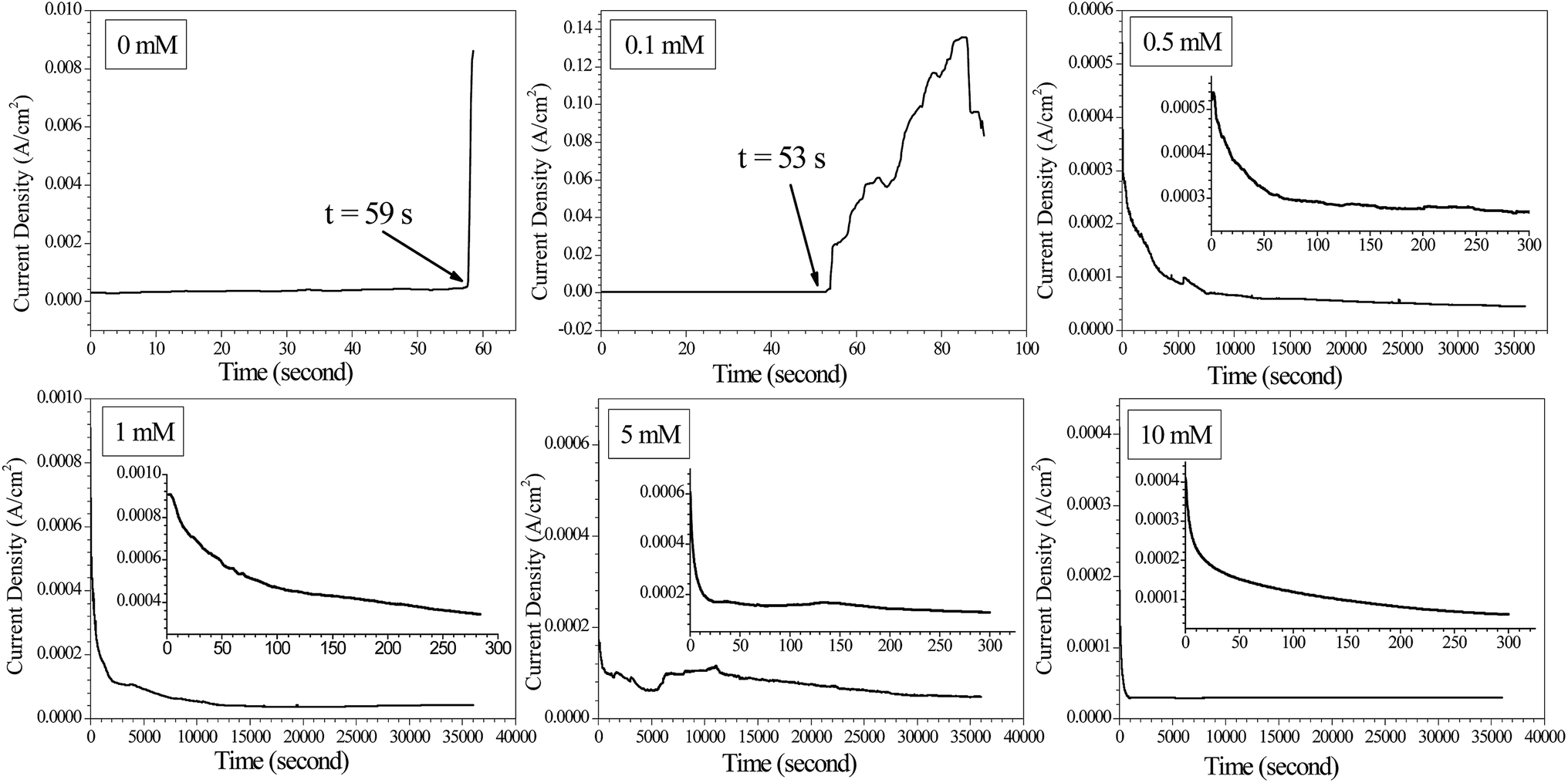
Current density vs. time curves during ECM tests with tin in 200 μm-thick electrolyte layers containing a varying concentration of Na2S and 1 mM Cl− at 3 V are shown in Fig. 1. The current transients measured between the two electrodes when bias voltages were applied between them show that the sharp increase in current was due to a short circuit occurring when dendrites joined the two electrodes.31 Sudden current spikes appeared without Na2S addition and with 0.1 mM Na2S. The time to short circuit decreased from about 59 s without Na2S to about 53 s in the presence of 0.1 mM Na2S. As the concentration of Na2S increased from 0.5 mM to 10 mM, no sudden current density spikes occurred at a 3 V bias voltage during a 10 h test, thereby indicating that dendrites did not bridge the two electrodes.
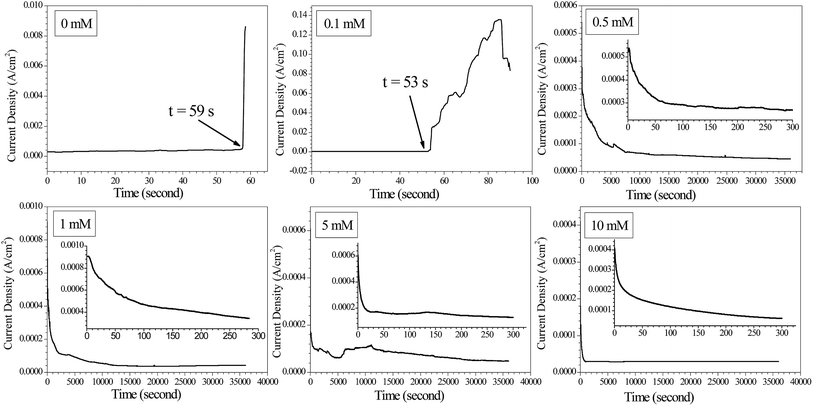 |
| | Fig. 1 Current density vs. time curves for the ECM of tin in 200 μm-thick electrolyte layers containing 1 mM Cl− and varying concentrations of Na2S at a 3 V bias voltage. | |
Fig. 2 shows current density vs. time curves during ECM tests with tin in 200 μm-thick electrolyte layers containing a varying concentration of Na2S and 1 mM Cl− at a 5 V bias voltage. Sudden current density spikes occurred without Na2S and in the presence of 0.5 mM Na2S. The time to short circuit decreased with increasing applied bias voltage. For example, the time to short circuit in the absence of Na2S decreased from 59 s at a 3 V bias voltage to 22 s at a 5 V bias voltage. This finding suggested that the growth rate of dendrites increased as the bias voltage increased.29 However, no sudden current density spike appeared during a 10 h test with the addition of 5 mM Na2S, indicating that a higher Na2S concentration was required to inhibit dendrites from bridging the two electrodes as the bias voltage increased.
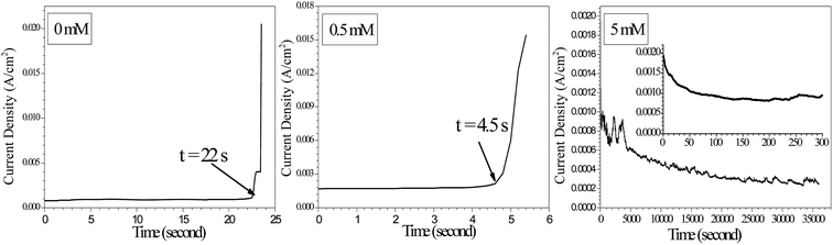 |
| | Fig. 2 Current density vs. time curves for the ECM of tin in 200 μm-thick electrolyte layers containing 1 mM Cl− and varying concentrations of Na2S at a 5 V bias voltage. | |
3.2. In situ optical observations of surface morphologies after ECM
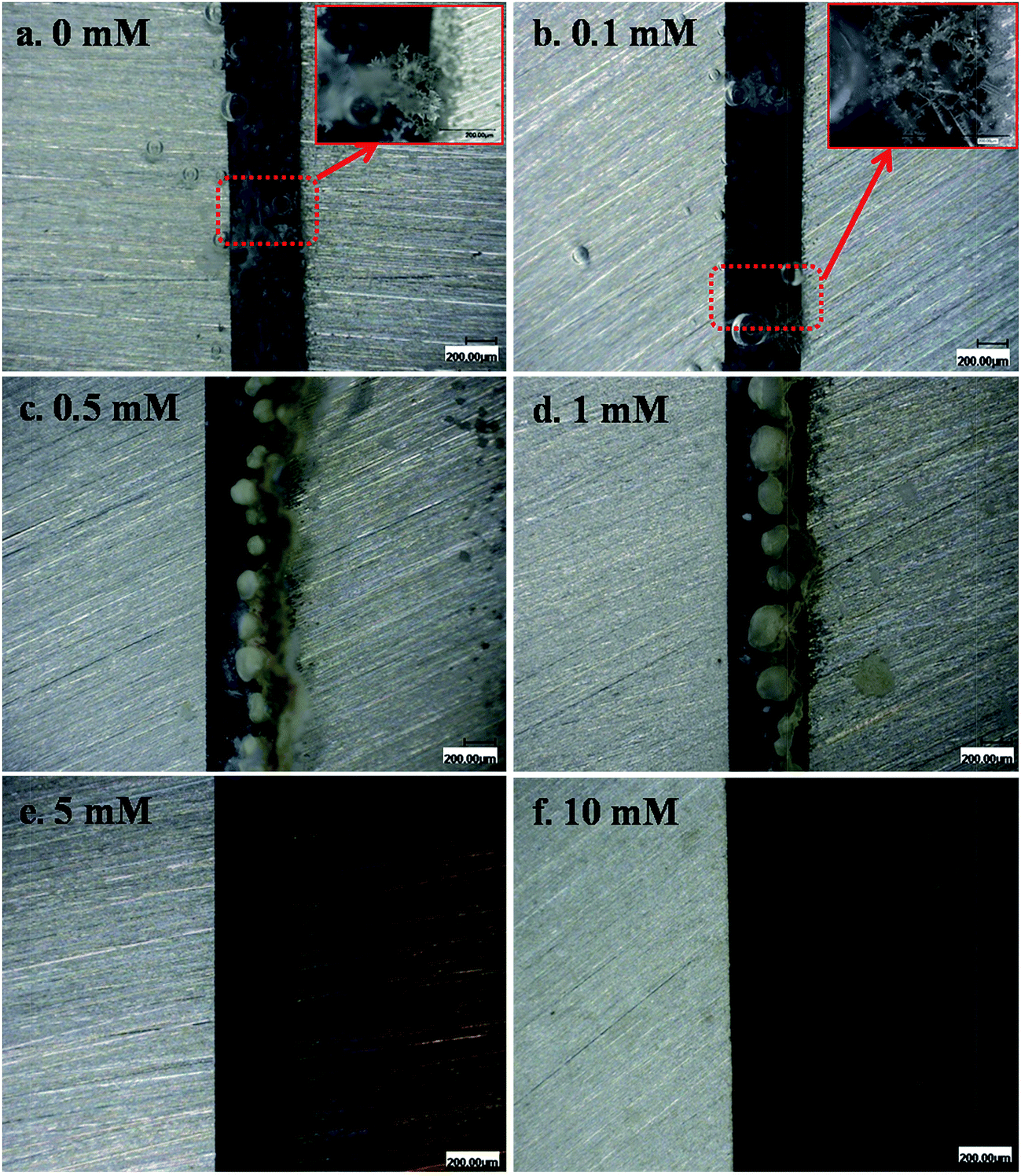
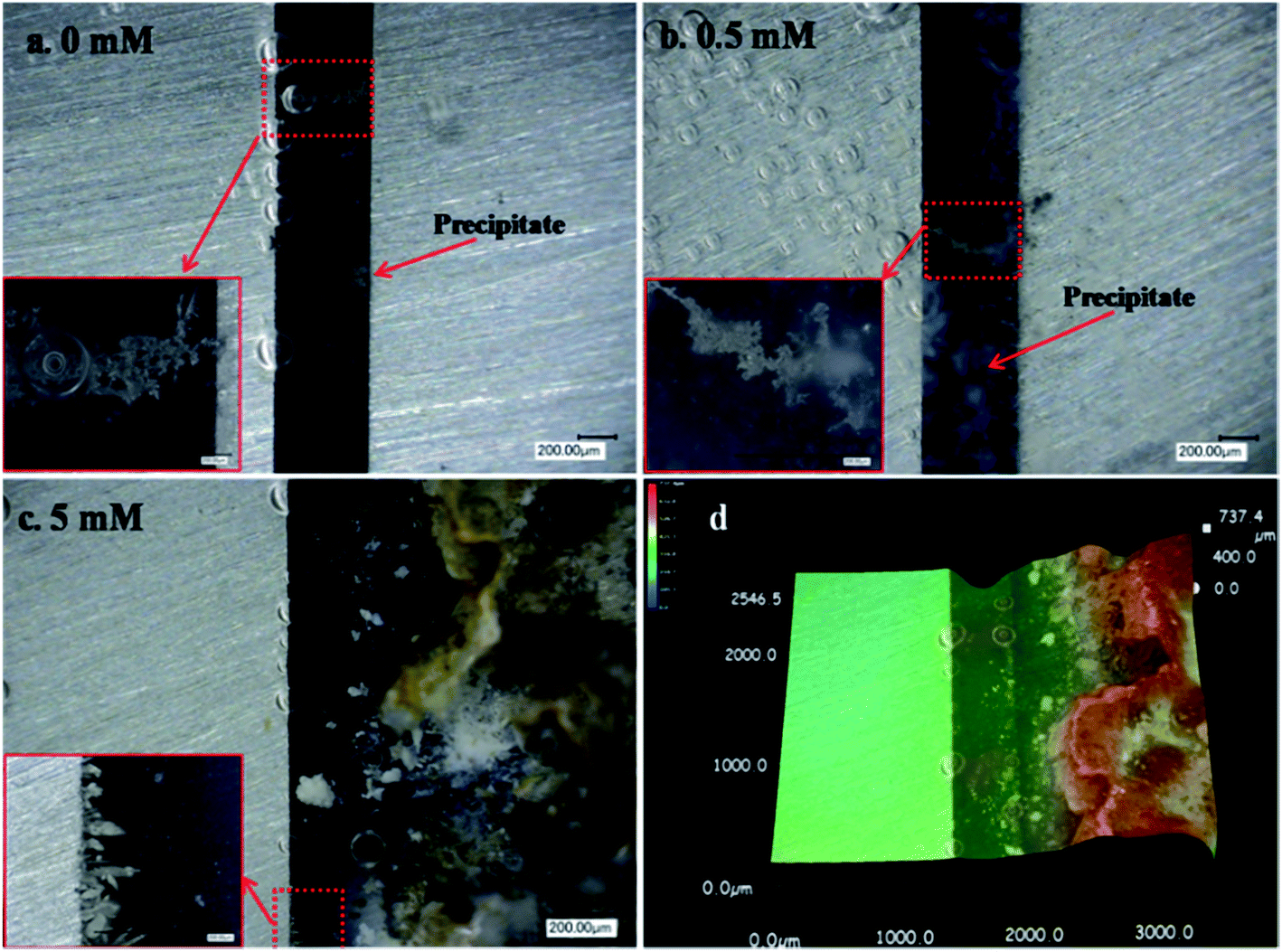
In situ optical observations were made on post-ECM electrode surfaces, as shown in Fig. 3 and 4. Tree- or needle-like dendrites accompanied by precipitates were observed in the absence of Na2S and the presence of 0.1 mM Na2S (Fig. 3a and b). With the addition of intermediate Na2S concentrations (0.5–1 mM), no dendrites were observed, but a large amount of white and yellow accumulated precipitate presented between both electrodes. At high Na2S concentration levels (5–10 mM), dendrites did not grow and the surfaces of the anodes darkened. When the bias voltage was increased to 5 V, dendrite growth was observed at intermediate and high Na2S concentration levels, as shown in Fig. 4b and c. Large amounts of dark and yellow precipitate were produced in the 10 h test in the presence of 5 mM Na2S at 5 V. The height of the accumulated precipitate was about 737.4 μm (Fig. 4d).
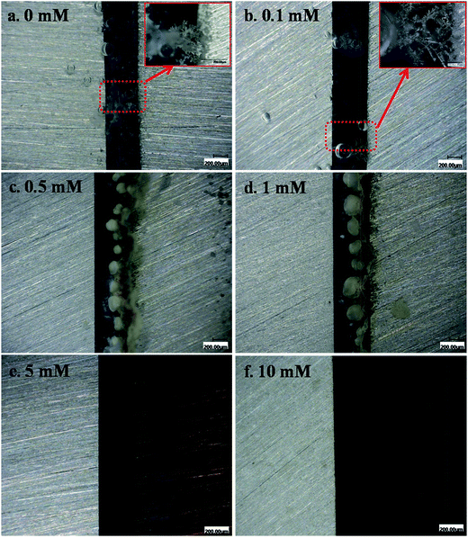 |
| | Fig. 3 In situ optical micrographs of the ECM of tin in 200 μm-thick electrolyte layers containing varying concentrations of Na2S and 1 mM Cl− at a bias voltage of 3 V over different time intervals: (a) 0 mM, 59 s; (b) 0.1 mM, 53 s; (c) 0.5 mM, 10 h; (d) 1 mM, 10 h; (e) 5 mM, 10 h; and (f) 10 mM, 10 h (the anode is on the right and the cathode is on the left). | |
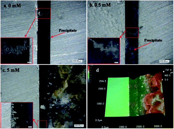 |
| | Fig. 4 In situ optical micrographs of the ECM of tin in 200 μm-thick electrolyte layers containing varying concentrations of Na2S and 1 mM Cl− at a bias voltage of 5 V over different time intervals: (a) 0 mM, 22 s; (b) 0.5 mM, 4.5 s; and (c and d) 5 mM, 10 h, with the corresponding 3D micrograph (the anode is on the right and the cathode is on the left). | |
3.3. Real-time pH distribution on the electrode surface during ECM
Fig. 5 displays some typical pictures extracted from in situ videos at varying time intervals to provide an overview of the local pH development in TELs containing 1 mM Cl− and varying concentrations of Na2S at a 3 V bias voltage. A universal pH indicator (pH 1–14) was added to the 200 μm-thick electrolyte layers to visualize pH development. The initial pH of the electrolyte increased with an increase in Na2S concentration. Upon applying a bias voltage, in the absence of Na2S, the electrolyte at the cathode became alkaline (blue in color), whereas that at the anode became acidic (bright yellow/orange in color) from 2 s to 30 s. The localized pH in the anodic area was close to 3. Similar phenomena were also observed at low and intermediate Na2S concentration levels. However, the electrolyte pH at the anode decreased to about 8 (green in color) within 30 s in the presence of high Na2S concentrations.
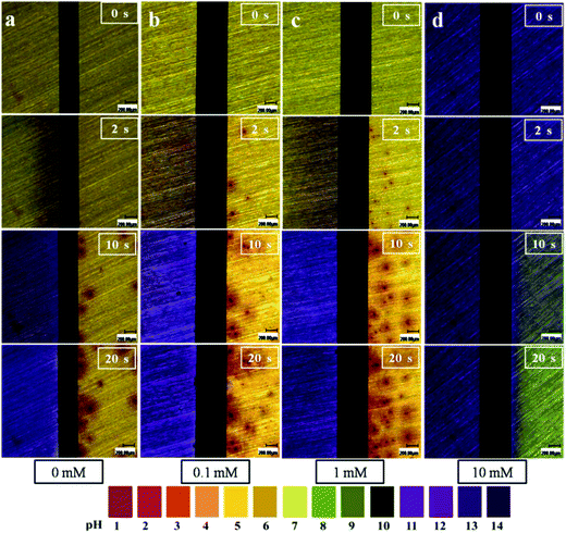 |
| | Fig. 5 Visualization of localized pH distribution on both electrodes using a pH indicator in 200 μm-thick electrolyte layers containing 1 mM Cl− and varying concentrations of Na2S at a 3 V bias voltage over different time intervals: (a) 0 mM; (b) 0.1 mM; (c) 1 mM; and (d) 10 mM (anode is on the right and cathode is on the left). | |
3.4. Characterization of dendrites and precipitates
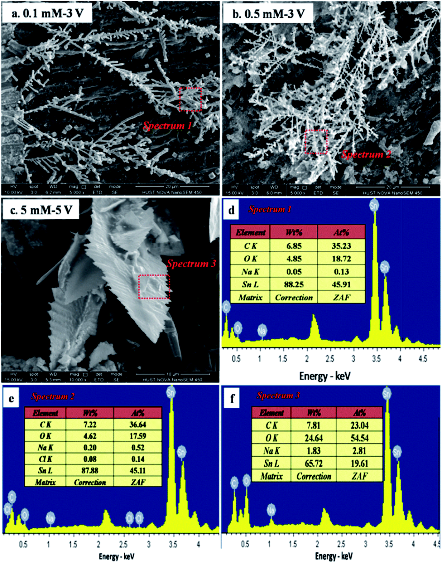
To obtain the microstructures and compositions of the dendrites and precipitates generated in the ECM process, characterization was performed using SEM, EDS, and XRD analyses. Fig. 6 shows SEM images and corresponding EDS spectra of dendrites after ECM tests in TELs with different Na2S concentrations at various bias voltages. In the presence of varying Na2S concentrations, the morphologies of the dendrites remained as tree-like or needle-like microstructures (Fig. 6a and b), similar to the structure of dendrites generated during ECM test in TELs containing 1 mM Cl−.29 EDS results further confirmed that the dendrites comprise metallic Sn, owing to the high atomic ratio of tin. When the bias voltage was increased to 5 V, the dendrites were covered with precipitate, and the branch or needle forms of the dendrites became coarser (Fig. 6c). The corresponding EDS spectrum (Fig. 6f) shows the increased atomic ratio of oxygen. These results illustrate that the addition of Na2S did not change the composition and microstructure of the dendrites. Fig. 7 shows the XRD patterns of samples obtained after ECM tests under different test conditions. The products mainly consisted of Sn2O3, Sn3S4, SnS, SnCl2, SnS2, Sn(SO4)2 and SnSO4.
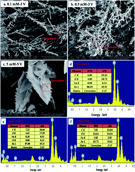 |
| | Fig. 6 SEM images of dendrites formed during the ECM of tin in 200 μm-thick electrolyte layers containing 1 mM Cl− and varying concentrations of Na2S at different bias voltages and the corresponding EDS spectra: (a) 0.1 mM, 3 V; (b) 0.5 mM, 5 V; and (c) 5 mM, 5 V; and (d) the EDS pattern for spectrum 1; (e) EDS pattern for spectrum 2; and (f) EDS pattern for spectrum 3. | |
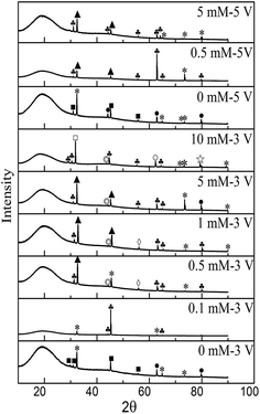 |
| | Fig. 7 XRD peaks for products formed during ECM in 200 μm-thick electrolyte layers containing 1 mM Cl− and varying concentrations of Na2S at different bias voltages: ■, Sn2O3; *, SnO; ●, Sn; ▲, Sn3S4; ♣, SnS; ◇, SnCl2; □, SnS2; ◎, Sn(SO4)2; and ☆, SnSO4. | |
4. Discussion
4.1. Basic reactions involved in the ECM of tin
The main anodic reactions for tin in TELs containing 1 mM Cl− are shown below:29,32| | |
2H2O → 4H+ + O2 + 4e−
| (3) |
Before dendrite growth, the main cathodic reactions include the reduction of water and dissolved O2 as shown in reactions (5) and (6) respectively:
| | |
2H2O + 2e− → H2 + 2OH−
| (5) |
| | |
O2 + 2H2O + 4e− → 4OH−
| (6) |
The pH distribution in Fig. 5a reveals that the localized pH in the anodic area was close to 3, which can be attributed to reactions (3), (7), and (8):2
| | |
Sn4+ + 4H2O = Sn(OH)4 + 4H+
| (7) |
| | |
Sn + 4H2O = Sn(OH)4 + 4H+ + 4e−
| (8) |
Sn(OH)4 dissolved to form [Sn(OH)6]2− under high OH− concentrations, as in reaction (9). The growth of dendrites can be attributed to the reduction of Sn2+, Sn4+, and/or [Sn(OH)6]2−:
| | |
Sn(OH)4 + 2OH− = Sn(OH)62−
| (9) |
| | |
[Sn(OH)6]2− + 4e− = Sn + 6OH−
| (12) |
4.2. Effect of Na2S on the ECM behavior of tin
White stannic and stannous hydroxide precipitates are reportedly generated after ECM tests in TELs containing 1 mM Cl−.29 However, in our case, a yellow precipitate formed in the presence of intermediate Na2S concentrations, whereas some black precipitate appeared upon the addition of high Na2S concentrations (Fig. 3), suggesting that the presence of Na2S changed the ECM behavior of tin. XRD results (Fig. 7) illustrate that some tin sulfate compounds were formed after ECM tests. According to a report by Lee A. Burton et al.,33 SnS is dark grey, SnS2 is yellow, and Sn2S3 is black, which agreed well with our observations. Different mechanisms for the formation of tin sulfate (SnS) have been postulated in the literature.34,35 In a proposed ion-by-ion mechanism, free Sn2+ ions react with S2− ions to form SnS (reaction (13)). In a hydroxide cluster mechanism, Sn2+ ions initially hydrolyze to form Sn(OH)2 clusters (reaction (14)), and then Sn(OH)2 reacts with S2− ions to form SnS clusters (reaction (15)).| | |
Sn2+ + 2H2O = Sn(OH)2 + 2H+
| (14) |
| | |
Sn(OH)2 + S2− = SnS + 2OH−
| (15) |
Simultaneously, Sn4+ ions can also react with S2− ions to form SnS2 (reaction (16)). K. Mishra et al.36 reported that the following candidates for the anodic corrosion of SnS are produced, as in reactions (17)–(21), when the samples are polarized at positive potentials in acidic electrolytes. We also observed that dark anodic corrosion ensued, in accordance with our results. Hence, the addition of Na2S precipitated tin ions on the anode and thereby retarded the formation of tin dendrites.
| | |
SnS + 2H+ = Sn2+ + S0
| (17) |
| | |
SnS + 2H+ + H2O = SnO + 2H+ + S0
| (18) |
| | |
SnS + 4H+ + 2H2O = SnO2 + 4H+ + S0
| (19) |
| | |
SnS + 2H+ + 6H2O = SnO2 + 2H+ + SO42−
| (21) |
4.3. Effect of Na2S concentration on the ECM behavior of tin
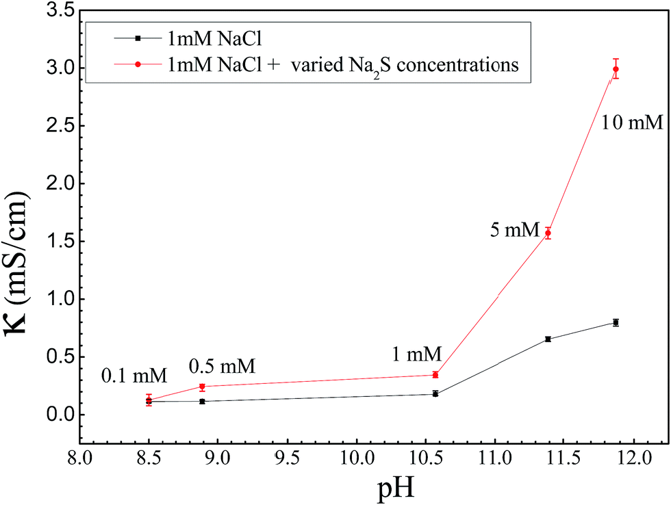
Anode dissolution caused by strong anodic polarization occurred, forming tin ions (Sn4+ and/or Sn2+). These then began to migrate from the anode to the cathode. Simultaneously, OH− produced at the cathode and S2− began to migrate toward the anode. SnS, SnS2, Sn(OH)4, and Sn(OH)2 were obtained as precipitates as soon as S2− and OH− met with Sn4+ and Sn2+ during the migration processes. Moreover, SnS and SnS2 may have been oxidized to SnO or SnO2 when they formed on the surface of the anode. Once the tin ions reached the cathode, dendrite growth occurred through preferential nucleation at some locations. During this process, the concentration of S2− played a great role in the ECM of tin. As shown in Fig. 8, the conductivity of the electrolyte increased with increasing Na2S concentration (i.e., 0.127 and 2.99 mS cm−1 for 1 and 10 mM Na2S, respectively). The initial rates of the anodic and cathodic reactions (reactions (1)–(6)) were accelerated because of the decrease in solution resistance. Reactions (reactions (13)–(15)) that involved S2− ions were also accelerated.
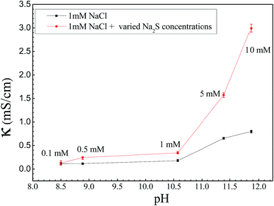 |
| | Fig. 8 Conductivity and pH of 1 mM NaCl with varying concentrations of Na2S, and the conductivity of 1 mM NaCl solution at the same pH. | |
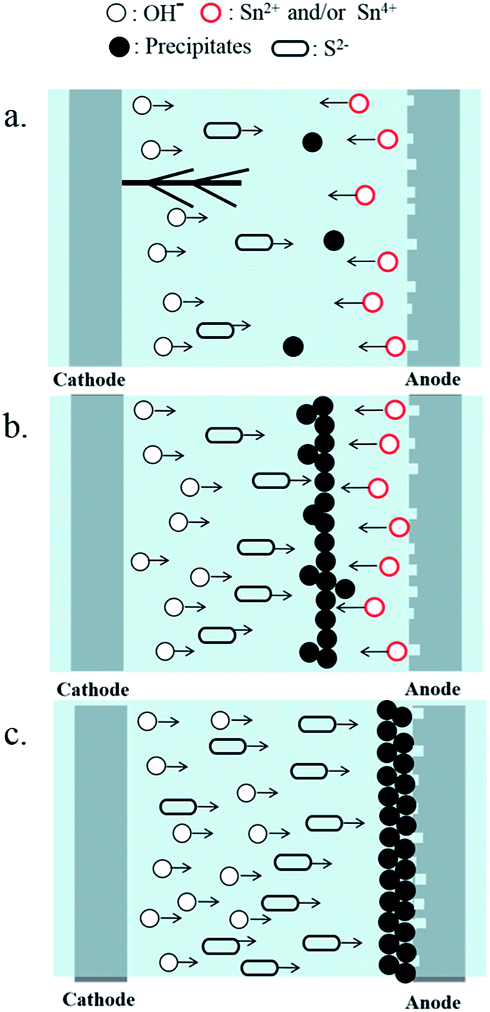
In the absence of Na2S and in the presence of low Na2S concentrations, dendrites accompanied by precipitates can be observed (Fig. 3a and b). The anodic dissolution of tin was promoted with the addition of Na2S, resulting in increased concentrations of Sn4+ and OH−. Reactions (9)–(12) were promoted. Thus, the time to short circuit decreased in the presence of low S2− concentrations, compared to without S2−.
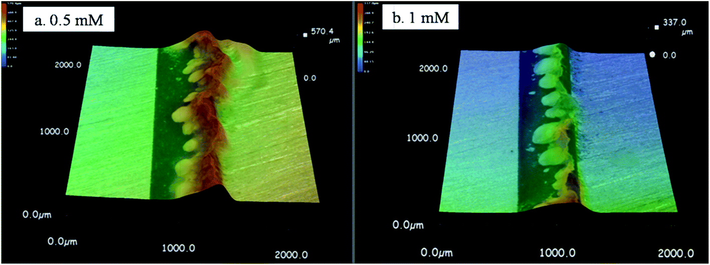
When the Na2S concentration increased to 0.5–1 mM, a large amount of white and yellow precipitates formed, but no dendrites grew (Fig. 3c and d). Fig. 10 shows 3D micrographs of the accumulated precipitates in the presence of intermediate Na2S concentrations; the height of the precipitate was 570 μm in the presence of 0.5 mM Na2S and 337 μm in the presence of 1 mM Na2S, both higher than the TEL. Accordingly, these precipitates can act as a wall-like barrier, retarding ion migration.30 The ion mobility is proportional to the charge of the ion and the reciprocal of ion size. The charge of S2− is twice that of OH−. However, the radius of an OH− ion is 0.137 nm and the radius of an S2− ion is 0.184 nm, which is less than twice that of OH−.37,38 In this case, the migration rate of S2− is higher than that of OH− under the same test conditions. And the yellow SnxSy precipitates were closer to the anode side. Meanwhile, the dissolution of precipitate (reaction (9)) still did not proceed because a higher pH was required. Therefore only precipitates, and no dendrites, were observed.
As the concentration of Na2S was further increased to 5–10 mM, higher concentrations of Sn2+ and OH− were produced rapidly, owing to the sharp increase in electrolyte conductivity (Fig. 8). Excess S2− ions reacted immediately with tin ions on the surface of the anode, and some tin sulfide was oxidized to stable tin oxide (reactions (18), (19), and (21)). In this case, tin ions were retarded to move to the cathode, and no dendrites grew (Fig. 9). Due to the formation of tin sulfide, the surface of the anode darkened (Fig. 3e and f).
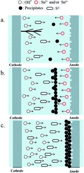 |
| | Fig. 9 Schematic diagram of the effect of Na2S concentration on the ECM behavior of tin: (a) at low Na2S concentrations; (b) at intermediate Na2S concentrations; and (c) at high Na2S concentrations. | |
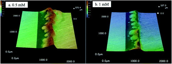 |
| | Fig. 10 3D micrographs of precipitates formed during the ECM of tin in 200 μm-thick electrolyte layers containing 1 mM Cl− and intermediate Na2S concentrations at a bias voltage of 3 V after 10 h: (a) 0.5 mM; and (b) 1 mM (the anode is on the right and the cathode is on the left). | |
4.4. Effect of pH alterations in the system owing to Na2S hydrolysis on the ECM behavior of tin
Na2S addition to an aqueous solution means an increase in the solution pH because of the hydrolysis reactions of S2− (reactions (22) and (23)). Thus, the initial pH values of TELs increased with increasing Na2S concentrations (Fig. 5).| | |
S2− + H2O = HS− + OH−
| (22) |
| | |
HS− + H2O = H2S + OH−
| (23) |
To understand the effect of initial pH on ECM, experiments were conducted in alkaline (adjusted using NaOH) environments. Fig. 8 shows that when the pH values of TELs containing 1 mM Cl− ions are the same as those of TELs containing 1 mM NaCl and a selected Na2S concentration, the conductivities of solutions with varying Na2S concentrations were higher than those with 1 mM NaCl.
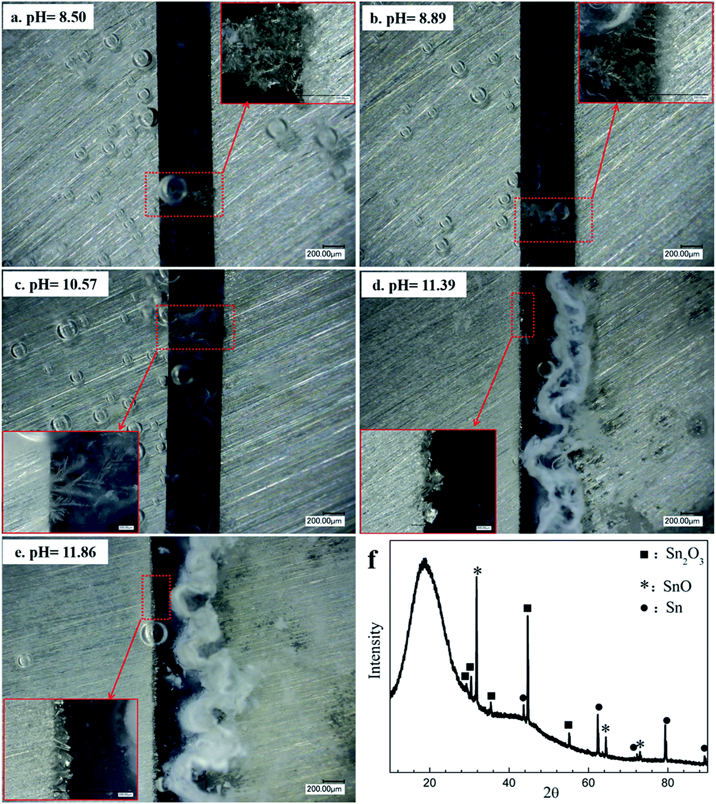
Fig. 11 shows current density vs. time curves during ECM tests with tin in 200 μm-thick electrolyte layers containing 1 mM Cl− with different initial pH values at a 3 V bias voltage. The time to short circuit increased with increasing pH. For example, the time to short circuit increased from about 42 s at pH 8.50 to about 53 s at pH 10.57, whereas no sudden current density spike occurred during a 10 h test at pH values of 11.39 and 11.86. As shown in Fig. 12d and e, a white heavy layer of precipitate formed on the anode at pH 11.39 and 11.86, and dense cubic dendrites formed on the cathode. Overall, the effects of pH suggested that the ECM of tin was pH dependent, and that a highly alkaline pH did not favor dendrite formation.
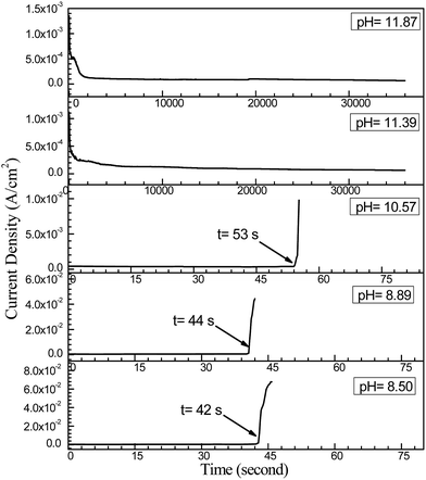 |
| | Fig. 11 Current density vs. time curves for the ECM of tin in 200 μm-thick electrolyte layers containing 1 mM Cl− with different initial pH values at a 3 V bias voltage. | |
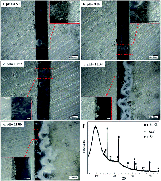 |
| | Fig. 12 In situ optical micrographs of the ECM of tin in 200 μm-thick electrolyte layers containing 1 mM Cl− with different initial pH values at a 3 V bias voltage over different time intervals: (a) pH 8.50, 42 s; (b) pH 8.89, 44 s; (c) pH 10.57, 53 s; (d) pH 11.39, 10 h; and (e) pH 11.86, 10 h (the anode is on the right and the cathode is on the left). (f) XRD peaks of products formed during ECM in 200 μm-thick electrolyte layers containing 1 mM Cl− at pH 11.86. | |
The presence of Na2S can cause the pH of TELs to increase. However, at intermediate Na2S concentration levels, dendrites did not bridge the two electrodes after 10 h and they caused a short circuit at 44 s in a TEL containing 1 mM Cl− at the same pH, indicating that the inhibition of Na2S on the ECM of tin was mainly due to the role of S2−. The micrographs in Fig. 3 and 12 confirm this observation, i.e., the presence of Na2S at high concentrations levels did not enable dendrite formation, which occurred only at high pH. Therefore, the inhibition effect of Na2S on the ECM of tin was due to S2−, which retarded the migration of tin ions from the anode to the cathode.
4.5. Effect of bias voltage on the role of Na2S in the ECM behavior of tin
Bias voltage, which is the driving force of ECM, evidently affects the role of Na2S on the ECM behavior of tin. As can be observed in Fig. 4, dendrites grew in the presence of 0.5 and 5 mM Na2S at a 5 V bias voltage, whereas no dendrites grew at a 3 V bias voltage. This finding can be attributed to the fact that a higher applied bias voltage results in faster anode dissolution and ion migration, and hence faster dendrite growth. Moreover, given the increase in the amount of tin ions, more S2− ions were required to precipitate the tin ions. Thus, as the concentration of Na2S increased to 5 mM at a 5 V bias voltage, no dendrites bridged the two electrodes after a 10 h test, indicating that the dendrite growth rate was slowed down in the presence of higher Na2S concentrations.
5. Conclusions
Na2S can retard the ECM behavior of tin in TELs containing chloride ions at a suitable concentration level.
(1) The inhibition effect of Na2S on the ECM of tin significantly depends on Na2S concentration. At low Na2S concentrations, tin dendrites grew faster than without Na2S. At intermediate Na2S concentrations, only precipitates but no dendrites existed. The accumulated precipitate acted as a wall-like barrier to retard ion migration. At high Na2S concentration levels, no dendrites but some tin sulfate precipitates formed on the anode surface. Excess S2− ions precipitated tin ions and thus prevented dendrite formation on the cathode.
(2) The applied bias voltage affected the role of Na2S in the ECM of tin. A higher Na2S concentration was required to retard the formation of tin dendrites. The time to short circuit decreased with increased applied bias voltage at intermediate Na2S concentration levels. At high Na2S concentration levels, the growth rate of tin dendrites slowed down at higher applied bias voltages.
Acknowledgements
The authors thank the financial support of the National Natural Science Foundation of China (No. 51571098) and analysis support from the Analytical and Testing Center, Huazhong University of Science and Technology.
References
- S. Zou, X. Li, C. Dong, K. Ding and K. Xiao, Electrochemical migration, whisker formation, and corrosion behavior of printed circuit board under wet H2S environment, Electrochim. Acta, 2013, 114, 363–371 CrossRef CAS.
- D. Minzari, M. S. Jellesen, P. Møller and R. Ambat, On the electrochemical migration mechanism of tin in electronics, Corros. Sci., 2011, 53, 3366–3379 CrossRef CAS.
- Y. Zhou and Y. Huo, The comparison of electrochemical migration mechanism between electroless silver plating and silver electroplating, J. Mater. Sci.: Mater. Electron., 2015, 27, 931–941 CrossRef.
- D. Li, P. P. Conway and C. Liu, Corrosion characterization of tin–lead and lead free solders in 3.5 wt% NaCl solution, Corros. Sci., 2008, 50, 995–1004 CrossRef CAS.
- K. M. Kumar, V. Kripesh and A. A. O. Tay, Influence of single-wall carbon nanotube addition on the microstructural and tensile properties of Sn–Pb solder alloy, J. Alloys Compd., 2008, 455, 148–158 CrossRef CAS.
- Y. Li, K.-S. Moon and C. Wong, Electronics without lead, Science, 2005, 308, 1419–1420 CrossRef CAS PubMed.
- N. Pewnim and S. Roy, Electrodeposition of tin-rich Cu–Sn alloys from a methanesulfonic acid electrolyte, Electrochim. Acta, 2013, 90, 498–506 CrossRef CAS.
- G. S. Mulugeta Abtew, Lead-free Solders in Microelectronics, Mater. Sci. Eng., R, 2000, 27, 95–141 CrossRef.
- B. Medgyes, B. Horváth, B. Illés, T. Shinohara, A. Tahara, G. Harsányi and O. Krammer, Microstructure and elemental composition of electrochemically formed dendrites on lead-free micro-alloyed low Ag solder alloys used in electronics, Corros. Sci., 2015, 92, 43–47 CrossRef CAS.
- B. Medgyes, B. Illés, R. Berényi and G. Harsányi, In situ optical inspection of electrochemical migration during THB tests, J. Mater. Sci.: Mater. Electron., 2011, 22, 694–700 CrossRef CAS.
- S.-B. Lee, Y.-R. Yoo, J.-Y. Jung, Y.-B. Park, Y.-S. Kim and Y.-C. Joo, Electrochemical migration characteristics of eutectic SnPb solder alloy in printed circuit board, Thin Solid Films, 2006, 504, 294–297 CrossRef CAS.
- X. Zhong, S. Yu, L. Chen, J. Hu and Z. Zhang, Test methods for electrochemical migration: a review, J. Mater. Sci.: Mater. Electron., 2017, 28, 2279–2289 CrossRef CAS.
- C. Dominkovics and G. Harsányi, Fractal description of dendrite growth during electrochemical migration, Periodica Polytechnica Electrical Engineering, 2009, 52, 13–19 CrossRef.
- D. Minzari, F. B. Grumsen, M. S. Jellesen, P. Møller and R. Ambat, Electrochemical migration of tin in electronics and microstructure of the dendrites, Corros. Sci., 2011, 53, 1659–1669 CrossRef CAS.
- B. Medgyes, B. Illés and G. Harsányi, Electrochemical migration behaviour of Cu, Sn, Ag and Sn63/Pb37, J. Mater. Sci.: Mater. Electron., 2012, 23, 551–556 CrossRef CAS.
- W. R. Osório, J. E. Spinelli, C. R. M. Afonso, L. C. Peixoto and A. Garcia, Microstructure, corrosion behaviour and microhardness of a directionally solidified Sn–Cu solder alloy, Electrochim. Acta, 2011, 56, 8891–8899 CrossRef.
- J.-Y. Jung, S.-B. Lee, Y.-C. Joo, H.-Y. Lee and Y.-B. Park, Anodic dissolution characteristics and electrochemical migration lifetimes of Sn solder in NaCl and Na2SO4 solutions, Microelectron. Eng., 2008, 85, 1597–1602 CrossRef CAS.
- X. Zhong, X. Guo, Y. Qiu, Z. Chen and G. Zhang, In Situ Study the Electrochemical Migration of Tin Under Unipolar Square Wave Electric Field, J. Electrochem. Soc., 2013, 160, D495–D500 CrossRef CAS.
- V. Verdingovas, M. S. Jellesen and R. Ambat, Influence of sodium chloride and weak organic acids (flux residues) on electrochemical
migration of tin on surface mount chip components, Corros. Eng., Sci. Technol., 2013, 48, 426–435 CrossRef CAS.
- B.-I. Noh and S.-B. Jung, Characteristics of environmental factor for electrochemical migration on printed circuit board, J. Mater. Sci.: Mater. Electron., 2008, 19, 952–956 CrossRef CAS.
- A. D. Subhendu, K. Panda, A. Dev, S. Gorai and S. Chaudhuri, Surfactant-Assisted Synthesis of SnS Nanowires Grown on Tin Foils, Cryst. Growth Des., 2006, 6, 2177–2181 Search PubMed.
- A. Redinger, D. M. Berg, P. J. Dale and S. Siebentritt, The consequences of kesterite equilibria for efficient solar cells, J. Am. Chem. Soc., 2011, 133, 3320–3323 CrossRef CAS PubMed.
- X. Chen, Y. Hou, B. Zhang, X. H. Yang and H. G. Yang, Low-cost SnS(x) counter electrodes for dye-sensitized solar cells, Chem. Commun., 2013, 49, 5793–5795 RSC.
- K. T. Ramakrishna Reddy, N. Koteswara Reddy and R. W. Miles, Photovoltaic properties of SnS based solar cells, Sol. Energy Mater. Sol. Cells, 2006, 90, 3041–3046 CrossRef CAS.
- A. H. B. Miller, Semiconductor liquid junction solar cells based on anodic sulphide films, Nature, 1976, 262, 680–681 CrossRef.
- M. Z. H. Zulkarnain Zainal and A. Ghazali, Cathodic electrodeposition of SnS thin films from aqueous solution, Sol. Energy Mater. Sol. Cells, 1996, 40, 347–357 CrossRef.
- L. O. D. S. B. Edério and D. Bidóia, The formation of anodic sulfide film on tin electrode, Corros. Sci., 1990, 31, 703–708 CrossRef.
- B. Sankapal, R. Mane and C. Lokhande, Successive ionic layer adsorption and reaction (SILAR) method for the deposition of large area (∼10 cm2) tin disulfide (SnS2) thin films, Mater. Res. Bull., 2000, 35, 2027–2035 CrossRef CAS.
- X. Zhong, G. Zhang, Y. Qiu, Z. Chen and X. Guo, Electrochemical migration of tin in thin electrolyte layer containing chloride ions, Corros. Sci., 2013, 74, 71–82 CrossRef CAS.
- B. Liao, Z. Chen and Y. Qiu, et al., Effect of citrate ions on the electrochemical migration of tin in thin electrolyte layer containing chloride ions, Corros. Sci., 2016, 112, 393–401 CrossRef CAS.
- O. Devos, C. Gabrielli, L. Beitone, C. Mace, E. Ostermann and H. Perrot, Growth of electrolytic copper dendrites. II: Oxalic acid medium, J. Electroanal. Chem., 2007, 606, 85–94 CrossRef CAS.
- X. Zhong, G. Zhang, Y. Qiu, Z. Chen, W. Zou and X. Guo, In situ study the dependence of electrochemical migration of tin on chloride, Electrochem. Commun., 2013, 27, 63–68 CrossRef CAS.
- L. A. Burton, D. Colombara, R. D. Abellon, F. C. Grozema, L. M. Peter, T. J. Savenije, G. Dennler and A. Walsh, Synthesis, characterization, and electronic structure of single-crystal SnS, Sn2S3, and SnS2, Chem. Mater., 2013, 25, 4908–4916 CrossRef CAS.
- P. Hankare, A. Jadhav, P. Chate, K. Rathod, P. Chavan and S. Ingole, Synthesis and characterization of tin sulphide thin films grown by chemical bath deposition technique, J. Alloys Compd., 2008, 463, 581–584 CrossRef CAS.
- C. Gao, H. Shen, L. Sun and Z. Shen, Chemical bath deposition of SnS films with different crystal structures, Mater. Lett., 2011, 65, 1413–1415 CrossRef CAS.
- K. Mishra, K. Rajeshwar, A. Weiss, M. Murley, R. D. Engelken, M. Slayton and H. E. McCloud, Electrodeposition and characterization of SnS thin films, J. Electrochem. Soc., 1989, 136, 1915–1923 CrossRef CAS.
- Y. Q. Jia, Crystal radii and effective ionic-radii of the rare-earth ions, J. Solid State Chem., 1991, 95, 184–187 CrossRef CAS.
- J. Vila, L. M. Varela and O. Cabeza, Cation and anion sizes influence in the temperature dependence of the electrical conductivity in nine imidazolium based ionic liquids, Electrochim. Acta, 2007, 52, 7413–7417 CrossRef CAS.
|
| This journal is © The Royal Society of Chemistry 2017 |
Click here to see how this site uses Cookies. View our privacy policy here. 
 Open Access Article
 This Open Access Article is licensed under a
  *ab and
Xingpeng Guoab
*ab and
Xingpeng Guoab