
 Open Access Article
 This Open Access Article is licensed under a
 Creative Commons Attribution 3.0 Unported Licence
Underlying mechanism of blue emission enhancement in Au decorated p-GaN film
Feifei Qin,
Ning Chang,
Chunxiang Xu *,
Qiuxiang Zhu,
Ming Wei,
Zhu Zhu,
Feng Chen and
Junfeng Lu
*,
Qiuxiang Zhu,
Ming Wei,
Zhu Zhu,
Feng Chen and
Junfeng Lu
State Key Laboratory of Bioelectronics, Department of Physics, Southeast University, Nanjing 210096, P. R. China. E-mail: xcxseu@seu.edu.cn; Tel: +86-025-83790755
First published on 7th March 2017
Abstract
Localized surface plasmons (LSPs) excited on metallic structures often play a significant role in mediating the photoluminescence (PL) of semiconductors. For p-GaN film, due to the LSP coupling, blue emission was enhanced while defect-related green emission was quenched to noise level after the decoration with Au nanoparticles (NPs). Why could the Au SP in the green light region enhance the blue and even ultraviolet emission? In this paper, a series of near/far-field spectral analyses and simulations were conducted to understand this process. A clear physical model of LSP-induced electron transfer was proposed to explain the defect-related LSP generation, coupling, electron transfer, and further blue emission increase with green emission reduction. Based on the PL measurement, an insulating SiO2 layer was introduced to confirm the LSP-induced electron transfer between Au and GaN. Additional green light was introduced to observe the LSP-induced PL enhancement, in the same way as for samples with defects. Our study provides a full understanding of the mechanism of PL enhancement in Au decorated GaN and this model should be universal for similar metal/semiconductor systems.
Introduction
The interaction between light and metal nanoparticles (NPs) induces collective oscillation of electrons and generates so-called localized surface plasmons (LSPs).1,2 In the past decade, surface plasmons of noble metals have attracted great attention relating to emission enhancement and lots of significant results have been reported.3–8 Among them, Au NPs were good candidates for enhancing photoluminescence (PL) of wide gap semiconductors with defect emission.9–11 Traditionally, reports about this are focused on Au/ZnO composites. For example, Li et al. observed 18-fold UV emission enhancement in Au coated ZnO film.12 In this case, it is possible to convert the useless defect radiation to useful exciton emission.13As a wide band-gap semiconductor with a high critical electric field and low intrinsic carrier concentration,14 GaN is one of the most promising materials for blue light emitting diodes (LEDs)15–17 and laser diodes (LDs).18,19 Since most devices composed of GaN materials work in the ultraviolet or blue range, it is very important to enhance the light emission at short wavelengths. As mentioned above, Au is an excellent material for PL modulation of wide gap semiconductors and it can convert the useless defect radiation to useful exciton emission. What will happen if we introduce LSP of Au NPs to GaN based materials? In fact, when decorating with Au, the blue emission of p-GaN was enhanced, while defect-related green emission was quenched to noise level. This can be attributed to LSP coupling between Au and GaN. However, the surface plasmon resonance position of Au NPs was generally located in the green region,20,21 while the PL enhancement appears in the blue or ultraviolet region. This means that the coupling condition was mismatched. Why could the Au SP in the green light region enhance the blue and even ultraviolet emission? The physical model of defect-related LSP generation, coupling, and electron transfer is not clear and the evidence for the enhancement mechanism is insufficient. It is very important to understand the mechanism of LSP-enhanced emission for the development of plasmon-related devices and applications.
In this paper, Au NPs were decorated to p-GaN film by a sputtering method, and blue emission was enhanced while defect-related green emission was quenched to noise level after the decoration with Au. Based on the near/far-field spectral analysis and simulation, a clear physical model of LSP-induced electron transfer was proposed to explain the defect-related LSP generation, coupling, electron transfer and further blue emission increase with green emission reduction. The method of introducing an SiO2 space layer was used to confirm the LSP-enhanced electron transfer of Au/p-GaN. Scanning near-field optical microscopy (SNOM) and finite difference time domain (FDTD) simulation were used to analyse the near-field properties of Au NPs. For GaN without defect emission, PL experiments were conducted to observe the LSP-induced PL enhancement, in the same way as for samples with defects, using an additional 532 nm laser to excite the LSP of Au. Our research provides a clear picture of the LSP-induced electron transfer mechanism and it can be further used to improve the understanding of PL enhancement in other metal-decorated semiconductor materials.
Experimental section
The heavily Mg-doped p-GaN films, which were purchased from Nano-Micro Tech Company, were deposited on a sapphire substrate with a thickness of about 4 μm. In order to compare the optical properties of p-GaN films before and after the decoration with Au NPs, they were cut into small pieces about 1 × 1 cm2 in area and then Au NPs were sputtered on them (Ion Sputter Hitachi E-1010) with different sputtering times of 0, 30, 60 and 90 s. The chamber pressure was fixed at 40 Pa, Ar was used as the carrier gas, and the sputtering current was fixed at 10 A. The space layer of SiO2 was sputtered using the radio frequency magnetron sputtering system. The chamber pressure of 2.0 Pa, Ar flow rate of 55 sccm, O2 flow rate of 5 sccm and the sputtering power of 100 W were fixed. A sputtering time of 300 s was used to get a space layer thickness of about 2.5 nm.The structural and morphological properties of the samples were characterized using X-ray diffraction (XRD-7000, Shimadzu) with Cu Kα radiation (λ = 0.15406 nm) and a field emission scanning electron microscope (FESEM, Carl Zeiss Ultra-Plus), which was equipped with an energy dispersive X-ray spectrometer (EDS) (OxfordX-Max50). Absorption measurements were carried out using a UV-vis-NIR spectrophotometer (Cary-5000, Varian). The PL spectra of the samples were measured using a fluorescence spectrophotometer (F-4600, Hitachi) with a Xe lamp as an excitation source at 325 nm. The excitation experiment with two sources was carried out using a 532 nm continuous crystal laser (power of 100 mW) as well as a 325 nm femtosecond pulsed laser (pulse duration of 150 fs, repetition rate of 1000 Hz), with the help of a fluorescence micro drive system. Scanning near-field optical microscopy (SNOM) results were recorded by a SNOM system (Multiview 400™). Moreover, our scattering-type SNOM is composed of an atomic force microscope (AFM) in which a metallized tip is illuminated with a focused 532 nm laser beam. All of the measurements were carried out at room temperature.
Results and discussion
Morphology and optical characterization
Fig. 1(a) shows the AFM images of the p-GaN film with and without SiO2 as a space layer. The observed amplitude value is 0.71 nm for bare p-GaN and 1.44 nm for p-GaN with SiO2, as depicted in Fig. 1(b). The same RMS value of about 0.46 nm for both films indicates the uniform sputtering of SiO2 on the p-GaN film. Fig. 1(c) shows the EDX spectrum and elemental mapping images of Au NP decorated p-GaN film, which confirm the presence of Ga, N, Mg, Si, O and Au. The inset of Fig. 1(c) shows an SEM image of the Au NPs which were sputtered on the surface of SiO2. The XRD patterns of the p-GaN films with and without a SiO2 layer are illustrated in Fig. 1(d). The XRD analysis revealed that the p-GaN film has a hexagonal crystal structure with diffraction planes of (1000), (0002), and (0004). The strongest diffraction peak corresponds to the diffraction plane of (0002) which indicates that the film mainly grew along the preferred direction of [0001]. After the sputtering of SiO2 as well as Au NPs, only a small peak of SiO2 around 17° is observed.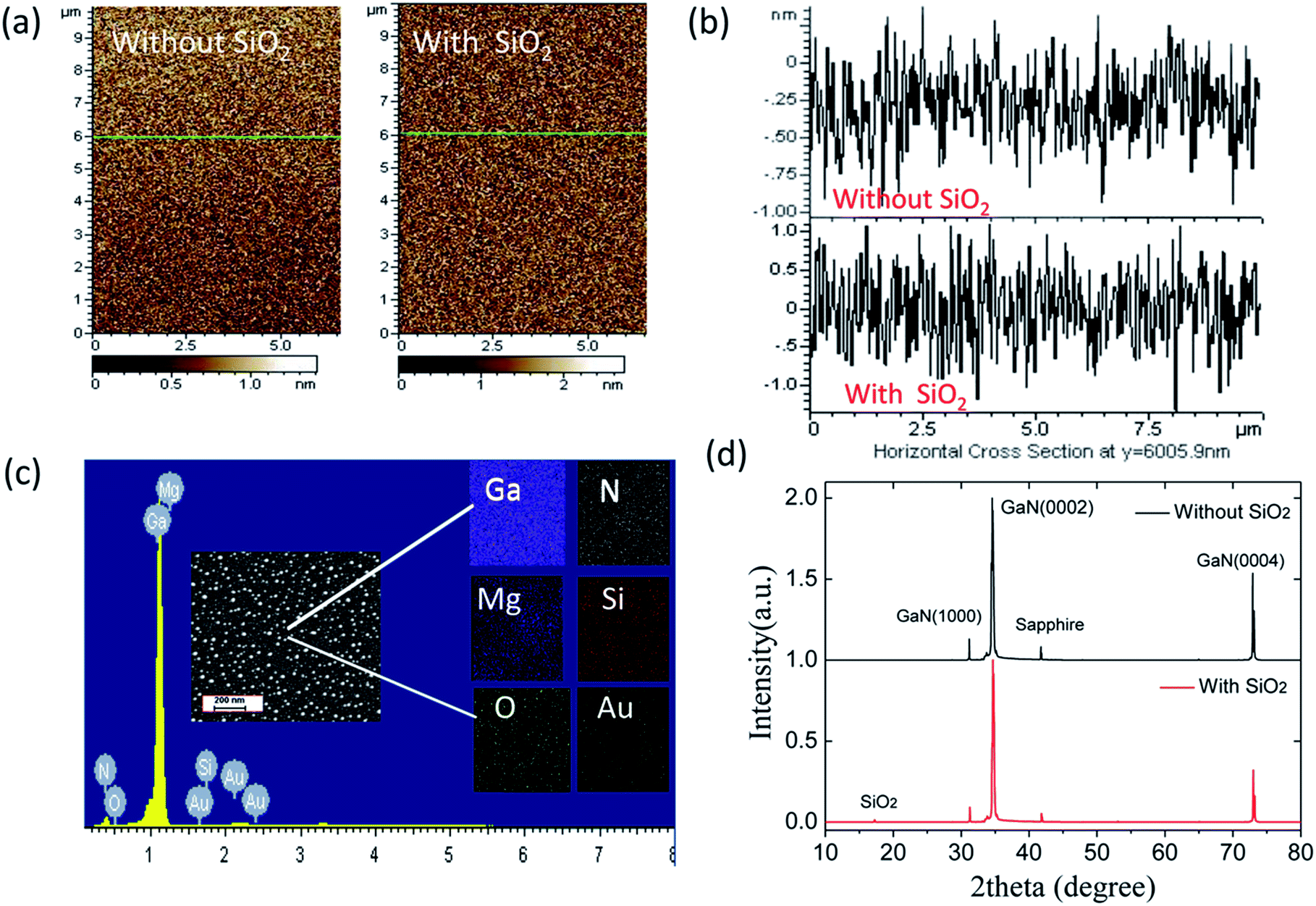 | ||
| Fig. 1 (a) AFM images of p-GaN film with and without an SiO2 layer, (b) surface information details of p-GaN with and without SiO2 from AFM in the position y = 6005.9 nm, (c) EDX spectrum and element mapping images of Au NP decorated p-GaN with SiO2, and (d) XRD patterns of p-GaN with and without SiO2. | ||
The PL spectra of p-GaN in Fig. 2(a) exhibit a blue emission at around 455 nm from donor–acceptor (D–A) pair recombination due to Mg doping, and an emission at around 547 nm, which is related to the defect of nitrogen vacancies.22–24 After the decoration with Au NPs, the blue emission of p-GaN is increased, while the green emission is suppressed to a noise level. In order to elucidate the effect of Au NPs on light emission, the Au nanoparticles have been decorated on p-GaN film with various sputtering times. Fig. 2(b) shows the relative intensity ratios of blue and defect emissions with respect to sputtering times. The film presented the strongest blue emission at a sputtering time of 60 s, about a 1.7 times greater enhancement when compared to that of bare p-GaN, and then it decreased with further increases in sputtering time. Furthermore, the defect-related emission declines with an increase in sputtering time and nearly reaches zero when further increasing the sputtering time to above 60 s. This phenomenon is mainly related to the size and space distributions of Au NPs and the degree of coupling of LSP.
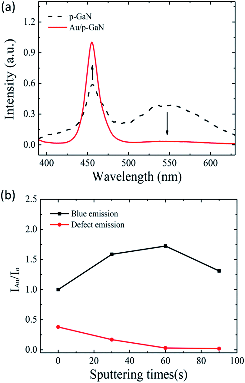 | ||
| Fig. 2 (a) PL spectra of p-GaN, with and without Au NPs, excited at 325 nm by a xenon lamp. (b) Relative intensity ratios of blue and defect emissions with respect to sputtering times. Here, IAu stands for the PL intensity of the Au decorated sample and Io stands for that of the undecorated sample. | ||
Understanding the mechanism of PL enhancement
To obtain a clear understanding of the PL enhancement shown in Fig. 2, the particle size distribution of Au, far-field optical absorption and local field information were explored and the results are depicted in Fig. 3 and 4. From the SEM images, Fig. 3(a)–(c), it can be identified that the diameters of the Au NPs are around 6–15 nm. When increasing the sputtering time, the diameter as well as the particle distribution density are also increased. In order to observe the LSP in real space, the localized Au plasmons have been visualized with a focused 532 nm laser beam using a scattering-type SNOM system.25,26 The image brightness corresponds to the local near-field coupling between the tip and sample, thus allowing us to directly observe the local field information. In addition, a clear light point and shade are noticed from Fig. 3(d) and (e), which implies that the localized Au plasmons can be excited by green light. Also, it gives direct evidence for excitation of LSP of Au NPs by the defect related emission of p-GaN. Fig. 3(f) shows the normalized optical absorption spectra of Au NPs with different sputtering times. The extinction peaks are presented at 528 nm, 550 nm and 565 nm for the sputtering times of 30 s, 60 s and 90 s respectively. Concomitantly, the photon energy of defect emission is very close to the surface plasmon resonance of Au NPs. So, Au is considered as a good absorber material for defect emission, as well as for the excitation of LSP. Quite interestingly, at the sputtering time of 60 s, the Au NPs have a strong absorption peak at around 550 nm, which is close to the photon energy for defect emission of p-GaN, located at around 547 nm. The energy of defect emission from p-GaN matched well with the LSP energy of Au NPs. Furthermore, the free electrons of Au NPs can be excited efficiently to a higher energy state. So, it has the best enhancement effect in the blue emission region. As the size of the Au NPs further increased with respect to sputtering time, the energy of defect emission deviated from the Au LSP energy. Due to this phenomenon, there is some decrement in coupling efficiency between the Au NPs and the p-GaN film, thus resulting in a lower enhancement factor at the sputtering time of 90 s.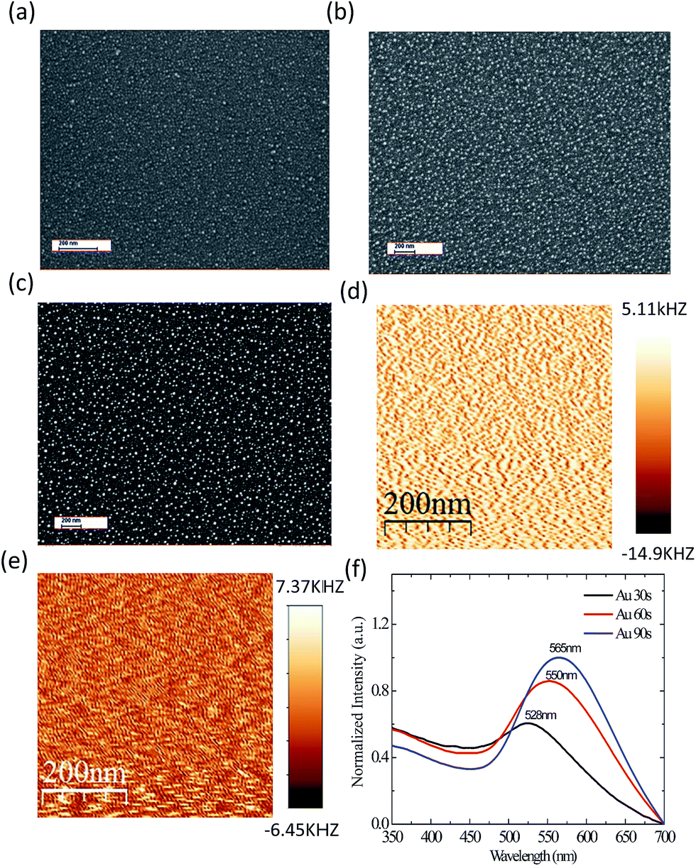 | ||
| Fig. 3 (a–c): Size and particle distributions of Au NPs with different sputtering times of 30 s, 60 s and 90 s, respectively. (d) Near-field image of Au NPs on p-GaN film. (e) Near-field image of Au NPs on p-GaN film with SiO2. (f) Normalized absorption spectra of Au NPs with different sputtering times. | ||
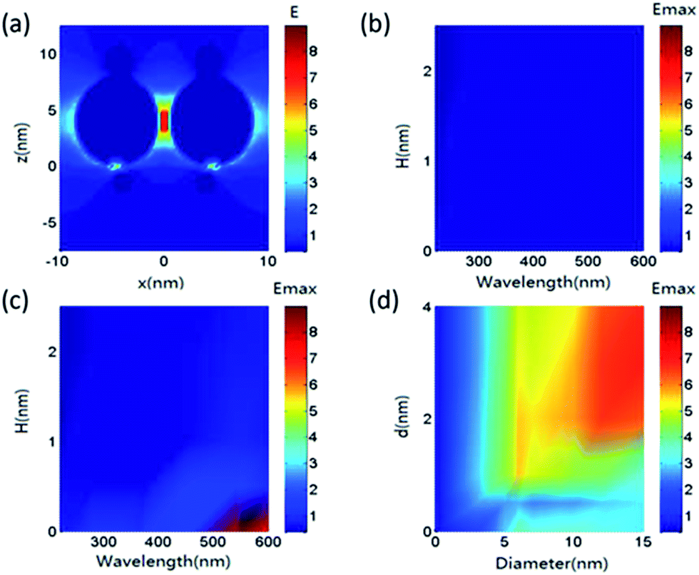 | ||
| Fig. 4 (a) Electric field along the z axis of multi-NP-decorated p-GaN film. (b) Maximum electric field intensity on the surface of GaN film with different thicknesses of SiO2. (c) Maximum electric field intensity on the surface of GaN film with different thicknesses of SiO2 and Au NPs (with a diameter of 10 nm and gap of 2 nm). (d) Maximum electric field intensity on the surface of GaN film with different Au diameters and particle gaps. Here, ‘H’ denotes the thickness of SiO2 and ‘d’ is the gap between two nearest Au particles. | ||
To further understand the relationship between PL enhancement and particle distributions, the properties of the local electromagnetic field for Au decorated GaN need to be considered, and the FDTD method is a well-known approach to deal with this.27,28 During the simulation, Au NPs with different sizes were put on the surface of GaN based materials. FDTD simulation was used to solve Maxwell equations in this situation and then the local electric field intensity was recorded. A perfectly matched layer (PML) boundary condition was used for the z axis direction and a period boundary condition was used for the x and y directions. A light source with wavelengths ranging from 200–700 nm was used to illuminate the samples in the z axis direction. An electric field monitor was used to record the electric field intensity. Electric field intensity charts are illustrated in Fig. 4. Comparing the data from Fig. 4(a) and (b), it can be observed that the distribution of Au NPs on the surface of the GaN film can cause a localized electric field enhancement. Due to a hotspot effect, a higher electric field enhancement can appear where the gap between two Au NPs is reduced.29 Fig. 4(c) shows the existence of an electric field enhancement even after the introduction of the SiO2 layer. For Au NPs, the highest enhancement effect appeared at a wavelength range of 500–600 nm, which agrees well with the absorption spectra in Fig. 3(f). In addition, since it is a localized evanescent field, heavy decay occurred along the z axis. For this reason, the SNOM image of Fig. 3(d) is clearer than that of Fig. 3(e). It is well-known that the LSP can be affected by the particle diameter as well as the particle distribution. To understand this, based on size parameters from the SEM images in Fig. 3, further calculations were carried out. The maximum local field intensity on the surface of the GaN and Au interface for diameters ranging from 0–15 nm and particle gaps ranging from 0–4 nm was simulated and the results are shown in Fig. 4(d).
From Fig. 4(d), it can be observed that the local electric field is increased with an increase in particle diameter as well as the particle gap of Au NPs. Also, a higher electric field area is present when the particle diameter ranges from 10–15 nm and the particle gap ranges from 2–4 nm. Furthermore, the LSP intensity can be described by the local electromagnetic field, so the above simulation results can be used to improve the understanding of PL enhancement and can be matched with the results in Fig. 2(a). From Fig. 4(a)–(c), it can be observed that the particle density increases with respect to sputtering time, which leads to an increase in hotspots, resulting in a higher local field enhancement. So the blue emission enhancement in Fig. 2(a) represents an increasing trend with a rise in sputtering time. However, when the particle density of Au was too high, it blocked the light propagation into the photo-detector, which resulted in a decrease in blue emission enhancement at the sputtering time of 90 s.
According to the above discussion, a model of the electron transfer mechanism is proposed. The schematic diagram of energy band alignment and the electron transfer process via LSP at the interface between the p-GaN film and Au NPs is illustrated in Fig. 5. According to the PL measurements and other researchers’ reports, the conduction band of p-GaN is located at −4.0 eV and the Fermi level of Au is located at −5.1 eV versus AVS. The defect-related emission can excite the surface plasmons of Au NPs which creates energetic electrons in higher energy states.29 These resonant electrons are very active and are transferred from the Au nanoparticles to the conduction band of p-GaN. After the relaxation process, the electron density in the donor level of p-GaN is significantly increased, which leads to an increase in the intensity of blue emission for the p-GaN film.
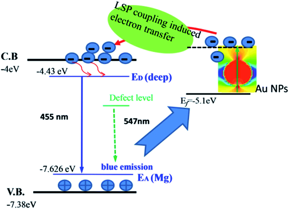 | ||
| Fig. 5 Energy band diagram of the p-GaN and Au compound system, showing the LSP coupling between p-GaN and Au NPs. | ||
Mechanism confirmation and the contribution of defect emission
To confirm the process of electron transfer, SiO2 has been introduced as space layer to block the electron transfer between the Au NPs and p-GaN film. When introducing a space layer of SiO2, the intensity of both blue and green emission is suppressed for all the sputtering times, as shown in Fig. 6. Based on the mechanism above, it can be suggested that the defect emission is suppressed by absorption and the space layer blocked the transfer of electrons between the Au NPs and the p-GaN film. In order to explore the effect of defect emission, a 532 nm continuous crystal laser and a 325 nm femtosecond pulsed laser beam were focused on undoped GaN film to obtain an experiment with two excitation sources, as shown in the inset of Fig. 7(b). Quite remarkably, from Fig. 7(a), it can be identified that there is no defect emission from GaN film when using the 325 nm fs laser as the excitation source. After the sputtering of Au NPs, the light emission of GaN is decreased. This behaviour can be understood by the fact that the electrons in Au particles are not able to reach higher energy states without surface plasmon resonance, thus resulting in no electron transfer from gold to the conduction band of GaN. When introducing an additional 532 nm laser to excite the LSP of Au NPs, the Au/GaN structure yielded a further PL enhancement as shown in the inset of Fig. 7(a). Moreover, the PL enhancement effect increased with respect to the incident power of the 532 nm laser for Au decorated GaN. This interesting phenomenon is shown in Fig. 7(b). It is well-known that more excitation power can provide more active electrons, and these can then be transferred to the conduction band. These results can make the mechanism of electron transfer more reliable.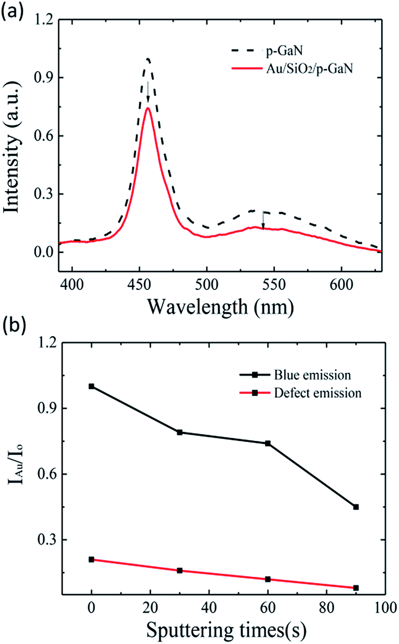 | ||
| Fig. 6 (a) PL spectra of p-GaN and p-GaN with Au NPs and SiO2 layer excited at 325 nm by a xenon lamp. (b) Relative intensity ratio of blue and defect emissions with respect to sputtering times. Here, IAu stands for the PL intensity of the Au decorated sample and Io stands for that of the undecorated sample. | ||
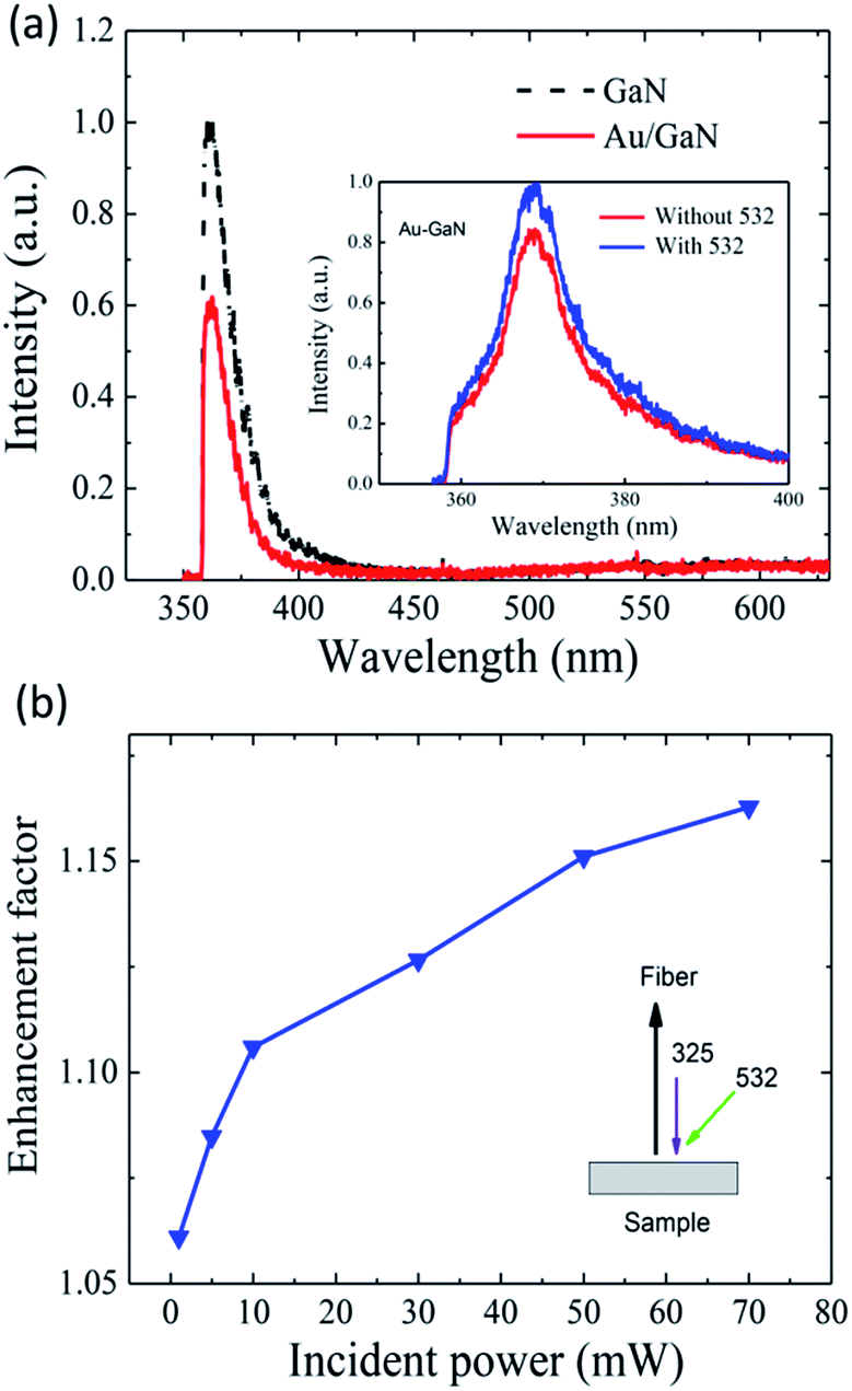 | ||
| Fig. 7 (a) PL spectra of different GaN samples excited by a 325 nm fs laser. The inset figure shows the PL spectra of Au decorated GaN by a double source excitation process. (b) PL enhancement factor for Au decorated p-GaN with different excitation powers of a 532 nm laser. The inset shows the schematic map of the double source excitation experiment. Here, a 325 nm laser was fixed as the first source to excite the PL of the samples, and a 532 nm laser was fixed as another source to excite the LSP of Au NPs. | ||
Conclusions
In summary, Au NPs were decorated to p-GaN films. Blue emission intensity is enhanced, while defect-related green emission is suppressed to noise level after the decoration with Au NPs. By introducing a SiO2 space layer, the mechanism was confirmed to be LSP induced electron transfer between the Au NPs and the p-GaN film. A series of near/far-field spectral analyses and simulations imply that the particle size and distribution of Au NPs have a strong influence on the LSP intensity, resulting in different enhancement effects. Observation of near-field properties in real space with SNOM gives sufficient evidence for the existence of LSP. Furthermore, for GaN without defect emission, PL enhancement was observed when introducing additional green light, which expounds the contribution of defect emission for the PL enhancement. Our results provided a clear understanding of light emission enhancement for Au NP-decorated p-GaN, and the proposed mechanism is also applicable for PL enhancement of other metal nanoparticle-decorated semiconductor compound systems.Acknowledgements
This work was supported by NSFC (61275054, 61475035) Jiangsu Province Science and Technology Support Program (BE2016177) and Collaborative Innovation Center of Suzhou Nano Science and Technology.Notes and references
- K. Manthiram and A. P. Alivisatos, J. Am. Chem. Soc., 2012, 134, 3995–3998 CrossRef CAS PubMed.
- H.-M. Bok, K. L. Shuford, S. Kim, S. K. Kim and S. Park, Nano Lett., 2008, 8, 2265–2270 CrossRef CAS PubMed.
- A. Neogi, C. W. Lee, H. O. Everitt, T. Kuroda, A. Tackeuchi and E. Yablonovitch, Phys. Rev. B: Condens. Matter Mater. Phys., 2002, 66, 153305–153309 CrossRef.
- K. Okamoto, I. Niki, A. Shvartser, Y. Narukawa, T. Mukai and A. Scherer, Nat. Mater., 2004, 3, 601–605 CrossRef CAS PubMed.
- M. Ringler, A. Schwemer, M. Wunderlich, A. Nichtl, K. Kuerzinger, T. A. Klar and J. Feldmann, Phys. Rev. Lett., 2008, 100, 203002–203006 CrossRef CAS PubMed.
- Y. Zang, X. He, J. Li, J. Yin, K. Li, C. Yue, Z. Wu, S. Wu and J. Kang, Nanoscale, 2013, 5, 574–580 RSC.
- K. W. Liu, Y. D. Tang, C. X. Cong, T. C. Sum, A. C. H. Huan, Z. X. Shen, L. Wang, F. Y. Jiang, X. W. Sun and H. D. Sun, Appl. Phys. Lett., 2009, 94, 151102–151104 CrossRef.
- P. Cheng, D. Li, Z. Yuan, P. Chen and D. Yang, Appl. Phys. Lett., 2008, 92, 041119–041121 CrossRef.
- S. L. Qu, C. J. Zhao, X. W. Jiang, G. Y. Fang, Y. C. Gao, H. D. Zeng, Y. L. Song, J. R. Qui, C. S. Zhu and K. Hirao, Chem. Phys. Lett., 2003, 368, 352–358 CrossRef CAS.
- C. W. Cheng, E. J. Sie, B. Liu, C. H. A. Huan, T. C. Sum, H. D. Sun and H. J. Fan, Appl. Phys. Lett., 2010, 96, 071107–071110 CrossRef.
- Y. Lin, C. Xu, J. Li, G. Zhu, X. Xu, J. Dai and B. Wang, Adv. Opt. Mater., 2013, 1, 940–945 CrossRef.
- X. Li, Y. Zhang and X. Ren, Opt. Express, 2009, 17, 8735–8740 CrossRef CAS.
- H. Y. Lin, C. L. Cheng, Y. Y. Chou, L. L. Huang, Y. F. Chen and K. T. Tsen, Opt. Express, 2006, 14, 2372–2379 CrossRef CAS PubMed.
- S. J. Pearton, J. C. Zolper, R. J. Shul and F. Ren, J. Appl. Phys., 1999, 86, 1–78 CrossRef CAS.
- Y. Takashima, M. Tanabe, M. Haraguchi and Y. Naoi, Opt. Commun., 2016, 369, 38–43 CrossRef CAS.
- Z. Sun, D. Teng, L. Liu, X. Huang, X. Zhang, K. Sun, Y. Wang, N. Chi and G. Wang, IEEE Photonics J., 2016, 8, 7904308–7908315 Search PubMed.
- D.-H. Kim, C.-O. Cho, Y.-G. Roh, H. Jeon, Y. S. Park, J. Cho, J. S. Im, C. Sone, Y. Park, W. J. Choi and Q. H. Park, Appl. Phys. Lett., 2005, 87, 203508–203510 CrossRef.
- M. T. Hardy, C. O. Holder, D. F. Feezell, S. Nakamura, J. S. Speck, D. A. Cohen and S. P. DenBaars, Appl. Phys. Lett., 2013, 103, 081103–081106 CrossRef.
- J. S. Kwak, J. Cho, S. Chae, K. K. Choi, Y. J. Sung, S. N. Lee, O. H. Nam and Y. Park, Phys. Status Solidi A, 2002, 194, 587–590 CrossRef CAS.
- Y. Nishijima, K. Ueno, Y. Yokota, K. Murakoshi and H. Misawa, J. Phys. Chem. Lett., 2010, 1, 2031–2036 CrossRef CAS.
- C. Langhammer, Z. Yuan, I. Zoric and B. Kasemo, Nano Lett., 2006, 6, 833–838 CrossRef CAS PubMed.
- U. Kaufmann, M. Kunzer, M. Maier, H. Obloh, A. Ramakrishnan, B. Santic and P. Schlotter, Appl. Phys. Lett., 1998, 72, 1326–1328 CrossRef CAS.
- M. A. Reshchikov and H. Morkoç, J. Appl. Phys., 2005, 97, 061301 CrossRef.
- M. A. Reshchikov, G. C. Yi and B. W. Wessels, Phys. Rev. B: Condens. Matter Mater. Phys., 1999, 59, 13176–13183 CrossRef CAS.
- R. Hillenbrand, T. Taubner and F. Keilmann, Nature, 2002, 418, 159–162 CrossRef CAS PubMed.
- N. Ocelic, A. Huber and R. Hillenbrand, Appl. Phys. Lett., 2006, 89, 101124–101127 CrossRef.
- F. Hao and P. Nordlander, Chem. Phys. Lett., 2010, 489, 141 CrossRef CAS.
- J. K. Yoon, K. Kim and K. S. Shin, J. Phys. Chem. C, 2009, 113, 1769–1774 CAS.
- C. Sonnichsen, T. Franzl, T. Wilk, G. von Plessen, J. Feldmann, O. Wilson and P. Mulvaney, Phys. Rev. Lett., 2002, 88, 077402–077405 CrossRef CAS PubMed.
| This journal is © The Royal Society of Chemistry 2017 |