
 Open Access Article
 This Open Access Article is licensed under a Creative Commons Attribution-Non Commercial 3.0 Unported Licence
Hybrid silicon–carbon nanostructures for broadband optical absorption†
Wen-Hua Yang*a,
Wen-Cai Lu *ab,
K. M. Hoc and
C. Z. Wangc
*ab,
K. M. Hoc and
C. Z. Wangc
aCollege of Physics and Laboratory of Fiber Materials and Modern Textile, Growing Base for State Key Laboratory, Qingdao University, Qingdao, Shandong 266071, P. R. China. E-mail: yangwh@qdu.edu.cn; wencailu@jlu.edu.cn
bInstitute of Theoretical Chemistry, Jilin University, Changchun, Jilin 130021, P. R. China
cAmes Laboratory-U.S. DOE, Department of Physics and Astronomy, Iowa State University, Ames, IA 50011, USA
First published on 25th January 2017
Abstract
Proper design of nanomaterials for broadband light absorption is a key factor for improving the conversion efficiency of solar cells. Here we present a hybrid design of silicon–carbon nanostructures with silicon clusters coated by carbon cages, i.e., Sim@C2n for potential solar cell application. The optical properties of these hybrid nanostructures were calculated based on time dependent density function theory (TDDFT). The results show that the optical spectra of Sim@C2n are very different from those of pure Sim and C2n clusters. While the absorption spectra of pure carbon cages and Sim clusters exhibit peaks in the UV region, those of the Sim@C2n nanostructures exhibit a significant red shift. Superposition of the optical spectra of various Sim@C2n nanostructures forms a broad-band absorption, which extends to the visible light and infrared regions. The broadband adsorption of the assembled Sim@C2n nanoclusters may provide a new approach for the design of high efficiency solar cell nanomaterials.
Introduction
As an important global problem, the potential energy shortage has attached a lot of attention. Solar energy is a clean, safe energy, and it is the largest source of sustainable energy. Making efficient utilization of solar energy is key to the development of modern economy and society. While solar cell technologies have been developing for many years, widespread use of solar cells to convert light into electricity is still limited by either high cost or low efficiency.1 Reducing the cost and improving the efficiency of light-to-electricity conversion devices are highly desirable for effective utilization of solar energy.Silicon-based nanomaterials have attracted a lot of attention due to their low reflectivity for light, high carrier collection efficiency, and potential low cost.2–10 However, the optical properties and thus the efficiency of the photovoltaic devices can be strongly dependent on the shape and size of the nanostructures as well as the substrate materials on which the nanostructures are supported.11–18
In the past several years, considerable theoretical and experimental research have been devoted to enhancing the light absorption by designing difference Si-based nanostructures, such as nanowires,3 nanosphere,4,19–21 nanocylinders,5,14 nanocones,6,14 nanodomes7 and naoholes,8,9 etc. For example, silicon nanocylinder arrays were designed and fabricated,5 total reflectance spectroscopy showed an average reflectivity of only 1.3% for light in the wavelength of 450–900 nm range. Wang et al. investigated the optical properties of Si nanocones arrays with various heights and diameters.14 They showed that Si naocones arrays can strongly interact with the incident light and the absorbance, and optical absorption over 95% for light in the wavelength of 300–2000 nm region can be achieved. Lin et al. designed the inverted nanopencils,22 which can reduce the optical reflection below 5% over the 400–1000 nm range and a wide angle of incidence between 0° and 60°. A novel silicon nano-conical-frustum array structure were successfully fabricated by Lu et al., which exhibits the absorbance of ∼99% over 400–1100 nm range.23 In addition, silicon nanosphere on a high-index substrate shows the a narrow-band antireflection properties in the visible spectral range.20,21 Recently, Ramon et al. designed the all-dielectric metasurfaces composed of silicon nanodisks which exhibit a generalized Brewster's effect,24 i.e. a zero of light reflection, at any angle of incidence light, frequency and polarization. These studies demonstrate that proper design of nanostructures is a key factor to improve the optical property, thus the conversion efficiency of solar cells.
Although Si nanoclusters have attracted a lot of theoretical and experimental interests due to their promising light emitting properties, it was shown that the optical properties of Si nanoclusters are strongly influenced by the surface passivation.25–35 Li et al. reported that acrylic acid coated Si nanoclusters have good photo luminescent stability.31 The molar extinction coefficient of Si nanoclusters is affected significantly by passivated alkyl and amine.32,33 Oxidized surface of Si nanoclusters also affect the optical property, especially red shift phenomenon were observed after Si nanoclusters are exposed to air.34 Zhou et al. studied the influence on luminescence from the hydrogen passivation on Si nanoclusters.35 They found that blue luminescence can be attributed to strong quantum confinement in hydrogen passivated Si nanoclusters. On the other hand, using carbon cages as costing materials to protect clusters against external interference has been attracted a lot of attentions.36–41 In particular, carbon cage encapsulating Si, Co, and Fe nanoparticles have been successfully synthesized by experiments, recently.36–40 It has been shown that the carbon cage encapsulation not only acts as protective layer against cluster oxidation, the hybrid nanostructures formed by the carbon cage and the encapsulated nanoparticles can also exhibit interesting electronic structures and desirable properties for magnetic and battery applications.36–41
In the present paper, we propose a new design of Si-based nanostructures, i.e., carbon fullerene coated Si nanoclusters for improving the light absorption efficiency. We show that the hybrid silicon–carbon nanostructures provide an interesting system to study the interplay between the electronic structures of Si clusters and carbon fullerenes and the unique optical properties arisen from such interplay. While pure carbon cages and pure Si clusters exhibit strong optical absorptions at the ultraviolet (UV) or far UV region, the optical spectra of the hybrid silicon–carbon nanostructures have substantial red shift. In particular, we found that assembly of the hybrid silicon–carbon nanostructures exhibit significant the optical absorption in the visible light and infrared regions. Our present study points to a promising direction for the design of high efficiency solar cell nanomaterials.
Computational method
The hybrid silicon–carbon nanostructures were designed by enclosing silicon clusters into carbon cages, i.e., Sim@C2n. The structure optimization and total energy calculations were performed within the first-principles density functional theory (DFT) framework by using Gaussian 09 package.42 The lowest-energy structures of Si7–13 clusters were taken from ref. 43 and fully optimized at the B3LYP/6-31G(d) level. These structures have been demonstrated to be the ground-state structures of the free-standing Si7–13 clusters. The binding energy (per atom) and the HOMO–LUMO gaps of these free-standing clusters obtained from our calculations were summarized in Table S1 in the ESI.† The binding energy per atom is defined by Eb = [mE(Si) − E(Sim)]/m, where E(Sim) and E(Si) are the energies of Sim cluster and a single Si atom, respectively. It is clearly seen that Si10 cluster is most stable in the size range of m = 7–13, which agrees well with those reported in ref. 43. Four fullerenes, i.e., C60-Ih, C70-D5h, C76-D2 and C84-D2 cages, were chosen for the encapsulation of Sim (m = 7–13) clusters. These structures of Sim@C2n (m = 7–13, 2n = 60, 70, 76, and 84) have been fully relaxed by B3LYP/6-31G(d) calculations. The structures of the Si clusters inside cages have some distortions due to the interaction between the carbon atoms and the cages.In order to see more clearly the effects on the electronic structures and optical properties from the carbon coating rather than from the distortions of the silicon clusters in the hybrid Sim@C2n structures, we also studied another type of structures where the Si clusters can maintain their structures inside the cages, although these structures may not be the ground-state structures in their free-standing forms. Si7@C60-Ih belongs to both two types of structures. The lowest-energy Si7 cluster encapsulated into C60-Ih can also maintain the pentagonal bipyramid structure although the pentagonal ring was slightly buckled. Similarly, Si9-A@C70-D5h, and Si12-A@C84-D2 discussed below also belong to both two types of structures.
The optical absorption properties of the nanostructures were studied by time-dependent density functional theory (TDDFT) using Gaussian 09 package. The absorption energy is determined by the energy difference between those of the final excited state and the initial occupied state of the electron, and the intensity of the absorption peak is proportional to the oscillator strength between the two states. In the TDDFT theory, the electronic excitations are calculated starting from the Kohn–Sham (KS) orbital and their eigenvalues. Then, electronic excitations were evaluated under the framework of linear response theory.44 The Becke's three-parameters and Lee–Yang–Parr' gradient-corrected correlation hybrid functional (B3LYP) and 6-31G(d) basis sets were used for optical calculations. The oscillator strength is defined as 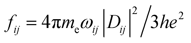 , where me, h and e are electron mass, Planck constant, and electron charge, respectively, ωij is angular frequency required to excite an electron from state i to state j, and Dij is transition dipole from state i to j. The excitation states included in the optical absorption for Sim, C2n and Sim@C2n are up to 6.2 eV, 5.48 eV and 4.30 eV from the HOMO, respectively.
We have assessed the accuracy of the TDDFT calculation for the optical properties of nanoclusters by comparing the results of optical gaps of the fullerenes from the TDDFT calculation with those from experimental measurement. The optical gaps of C60-Ih, C70-D5h, C76-D2 and C84-D2 cages from our TDDFT calculations are 2.28, 2.10, 1.08, and 1.44 eV respectively, which are reasonably in good agreement with experimental values of 1.9–2.3 eV, 1.6–1.95 eV, 1.36–1.4 eV, and 1.24 eV respectively.45–52 After the Si clusters have been inserted inside fullerenes, the HOMO–LUMO gaps of free C60-Ih (2.28 eV) and C70-D5h (2.10 eV) cages decrease to 1.20 and 0.89–1.99 eV, respectively, and the gaps of free C76-D2 (1.08 eV) and C84-D2 (1.44 eV) cages change to 1.03–1.29 and 0.88–1.52 eV, respectively.
Results and discussion
Structures
The structures of the endohedral fullerene Sim@C2n (m = 7–13, 2n = 60, 70, 76 and 84) after the optimization by DFT calculations are shown in Fig. 1. As one can see from Fig. 1, the fullerene cages are well preserved after the Sim clusters encapsulation, although the shape of the cages has some small distortion. By contrast, the deformation of the Sim clusters upon the encapsulation is more obvious. As shown in Fig. 1, free-standing Si7 cluster is a pentagonal bipyramid. Si7 encapsulated into C60-Ih can still maintain the pentagonal bipyramid structure although the pentagonal ring is slightly buckled. As the size of the fullerene cage increases, more deformation in the encapsulated Si7 cluster can be seen. In particular, one of the Si atoms deviates substantially from the pentagonal plane, as indicated by red color in Fig. 1, making the encapsulated Si7 transformed into a tetragonal bipyramid structure. The ground-state structures of free-standing Si8 and Si9 clusters are the derivatives of tetragonal bipyramid and pentagonal bipyramid, respectively, while that of free-standing Si10 cluster is a tricapped-trigonal-prism (TTP). When these Si clusters are enclosed into the carbon fullerene cages, there are noticeable deformations but the structures inside the carbon cages still resemble those of free-standing clusters. The structures of free-standing Si11 and Si13 clusters are also the derivatives from the TTP Si10. However, the encapsulated Si11 cluster transforms into a hollow cage while the Si13 cluster changes to an icosahedral structure similar to an Al13 cluster.53 The ground-state structure of free-standing Si12 cluster43 cannot be encapsulated into fullerene cage C2n (2n = 60, 70, 76, and 84) without substantial deformation due to its prolate shape. Thus we did not consider it in our study.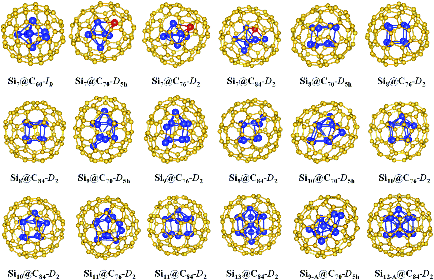 | ||
| Fig. 1 Structures of hybrid silicon–carbon nanostructures Si7–13@C2n (2n = 60, 70, 76, and 84). The Si atoms were denoted by blue and red colors, C atom was denoted yellow color. The structures were optimized using B3LYP/6-31G(d) method. | ||
In addition to the encapsulation of the ground-state free-standing clusters into the carbon cages, we have also searched for other Si clusters that can maintain their free-standing structures inside the cages so that effects of carbon cage can be seen more clearly. Two structures, Si9-A@C70-D5h and Si12-A@C84-D2, from our search are shown in Fig. 1. The structure of Si7@C60-Ih shown in Fig. 1 also belongs to this type of structure. As shown in Fig. 1, the Si9-A cluster encapsulated by the fullerene cage C70-D5h can be viewed as a pentagonal bipyramid capped by two atoms on the same side, while the free-standing Si9 cluster is a pentagonal bipyramid capped by two atoms on both sides. For Si12-A@C84-D2, the Si cluster takes an icosahedral-like structure with one top atom missed from a 13-atom icosahedral cluster, similar to the geometry of the Al12 cluster,53 different from the free-standing Si12 cluster with a prolate shape.
Electronic properties
To better understand the electronic properties, we analyzed the density of states (DOS) for the free-standing Sim and Sim@C2n clusters respectively. The electronic DOSs for the free-standing Si7 and Si7@C2n (2n = 60, 70, 76, and 84) clusters are shown in Fig. 2 (The DOSs of other free-standing and hybrid clusters are similar). The calculated DOSs were broadened by 0.2 eV using a Gaussian function. The Fermi energy level was set at 0.0 eV. The corresponding molecular energy levels of the nanostructures are also shown in Fig. 2. Compared with the DOS of free-standing Si7 cluster, obvious changes were observed in those of Si7@C2n. In particular, there are many energy levels located close to the Fermi energy level in the Si7@C2n as compared to that of Si7. The calculation results show that the HOMO–LUMO gaps of Si7@C60-Ih, Si7@C70-D5h, Si7@C76-D2 and Si7@C84-D2 are 1.10, 0.96, 1.39 and 1.40 eV, respectively, much smaller than the HOMO–LUMO gap of free-standing Si7 which is 3.18 eV. The red shift in the optical absorption spectra of the Sim@C2n cluster can be ascribed to the decrease of the energy gaps.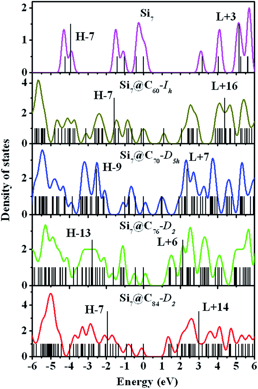 | ||
| Fig. 2 Comparison of electron density-of-states (DOS) and the corresponding energy levels of Si7 and Si7@C2n (2n = 60, 70, 76, and 84). | ||
Optical properties
The optical absorption spectra of the Sim and Sim@C2n clusters obtained from the TDDFT calculations are displayed in Fig. 3. The principle excitation energies and oscillator strengths of the free-standing and encapsulated clusters were given in Tables S2 and S3,† respectively, where the contributions of orbital-to-orbital transitions of more than 20% were listed.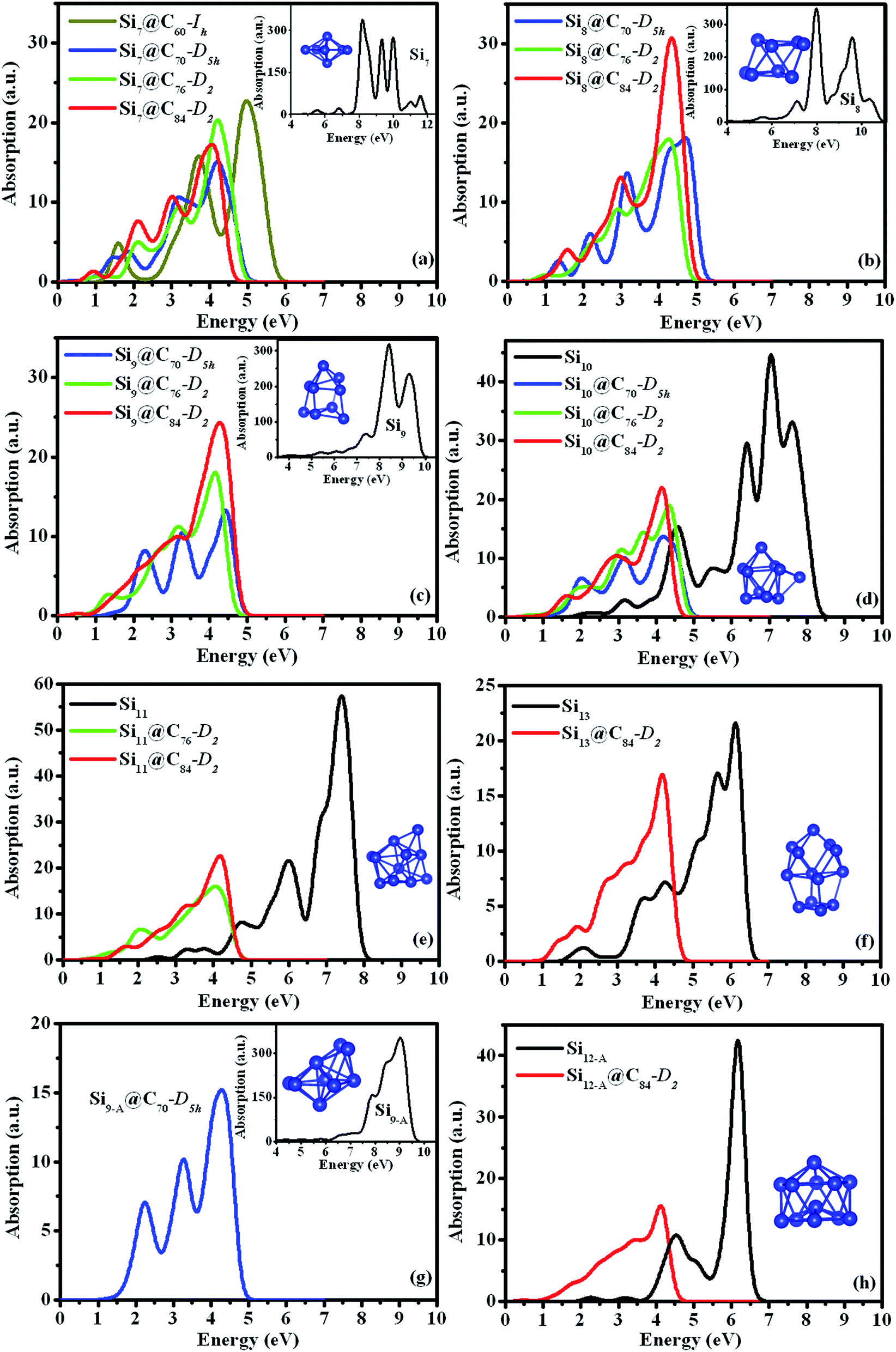 | ||
| Fig. 3 Optical absorption spectra of free-standing silicon clusters (black lines) compared with those of hybrid silicon–carbon nanostructures Si7–13@C2n (2n = 60, 70, 76, and 84) from the TDDFT/B3LYP/6-31G(d) calculations. Substantial red shift in the hybrid structures compared to that of free-standing silicon clusters can be clearly seen. | ||
As shown in Fig. 3, the optical absorption spectra of the Sim@C2n clusters exhibit a significant red shift in comparison with that of free-standing Sim clusters. Absorptions of the free-standing Sim clusters occur at 6.17–9.97 eV in the ultraviolet range, while those of the Sim@C2n occur at 1.90–5.34 eV. The structure of free-standing Si7 cluster has been well characterized by experiment and theory. As we can see from the insert in Fig. 3(a), the absorption spectrum of free-standing Si7 cluster shows a very sharp ultraviolet peak at the energy of 8.14 eV with an oscillation strength f = 2.302. The main contribution to this peak is from HOMO−7 to LUMO+3 transition. In comparison, the absorption intensity of the Si7@C2n clusters is reduced by a factor of 30 relative to that of the free-standing Si7 cluster. The absorption peaks in the Si7@C2n clusters is also dependent on the size of the fullerene cages, exhibiting significant red-shift as the size of the fullerene change from C60-Ih to C70-D5h. However, in Si7@C70-D5h, Si7@C76-D2 and Si7@C84-D2, their absorption spectra become similar with the strong peak almost at the same energies, which are about 4.33, 4.26 and 4.31 eV, respectively. Some dependence of absorption peaks on the size of fullerene is also seen for other Sim@C2n nanoparticles. Slight red-shift in the main adsorption peak as the size of the fullerene increase from 70 to 84 can also be seen for Si8@C2n, Si9@C2n and Si10@C2n as shown in Fig. 3(b)–(d).
We have also analyzed the optical properties of Si7@C60-Ih, Si9-A@C70-D5h and Si12-A@C84-D2. We found that in Si7@C60-Ih, two relatively sharp peaks at 3.76 eV and at 5.34 eV in the ultraviolet region, respectively, are primarily contributed from the transitions HOMO−1 → LUMO+15 and HOMO−7 → LUMO+16. The optical absorption spectrum of Si9-A@C70-D5h exhibits three peaks at 2.24 eV in the visible light region, and at 3.30 and 4.33 eV in the ultraviolet region, respectively. The absorption peak at 2.24 eV is dominated by the transitions HOMO−1 → LUMO+9 and HOMO → LUMO+10, while that at 3.30 eV and 4.33 eV are dominated by the transition HOMO−8 → LUMO+10 and HOMO−4 → LUMO+19, respectively. The optical absorption spectrum of Si12-A@C84-D2 is shown in Fig. 3(h). The main absorption peaks is at 4.16 eV in the ultraviolet region, which is dominated by the transition HOMO−18 → LUMO+6.
To further understand the optical property, it is worthwhile to analyze main transitions in detail. For example, some main transitions of Si7 and Si7@C2n were marked by the arrows in Fig. 2. The primary absorption peak of the free-standing Si7 is from HOMO−7 to LUMO+3 (8.14 eV). In Si7@C60-Ih, the strong peak lies at 5.34 eV, which is ascribed to the transition HOMO−7 → LUMO+16. In Si7@C70-D5h, Si7@C76-D2 and Si7@C84-D2, the strong peaks lie at 4.33, 4.26 and 4.31 eV, respectively, which are ascribed to HOMO−9 → LUMO+7, HOMO−13 → LUMO+6 and HOMO−7 → LUMO+14 transitions, respectively. The main features of optical excitations of Sim and Sim@C2n (m = 8–13, 2n = 70, 76 and 84) are similar to those of Si7 and Si7@C2n as shown in Fig. 2. These results show that the red shift of optical properties can be ascribed to the decrease of HOMO–LUMO gaps and the increase of the number of energy levels near Fermi level.
Broadband optical absorption
Electromagnetic radiation from sun spreads over a wide range of continuous spectrum, and the sun radiation intensity is also different for different wavelengths, as shown in the bottom panel of Fig. 4. Most Si-based solar cells are effective only in certain energy range in the solar spectrum due to the narrow-band optical absorption features of the solar cells. In designing more efficient solar cell materials, it is desirable to improve their absorption spectra in conformity with the solar radiation spectrum in the visible light region. For the free-standing Sim clusters, our TDDFT calculation results show that they are not efficient for solar cells because their optical absorptions have narrow peaks at the high-energy ultraviolet region as shown in the top panel of Fig. 4. In the experiment, it is shown that the absorption spectrum of fullerene cage C2n also does not appear in the visible light region,52,54–56 consistent with our calculated results for C60-Ih, C70-D5h, C76-D2 and C84-D2 cages as one can see from the top panel of Fig. 4. However, the optical absorption spectra of the hybrid silicon–carbon structures are very different from that of pure silicon or carbon nanostructures. Our present calculation demonstrates that the main optical absorption peaks of Sim@C2n clusters are between 1.90 to 5.34 eV, which spread over the range of the visible light region. By superposition of all the optical spectra of the Sim@C2n cluster from the present study as shown in the middle panel of Fig. 4, we can obtain a broadband absorption with the intensity extends substantially into the visible light and infrared regions. Therefore, assembled Sim@C2n would provide a new direction for the design of more efficient solar cell nanomaterials.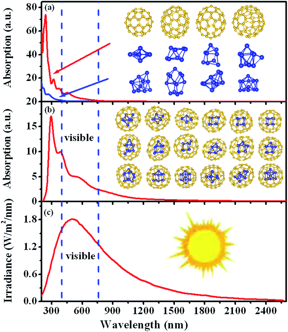 | ||
| Fig. 4 (a) Superposition of the optical absorption spectra of free-standing Si7–13 clusters (blue) and that of C60 + C70 + C76 + C84 cages (red). (b) Superposition of the optical spectra of the assemble of Sim@C2n and the spectrum of solar radiation shown in (c). | ||
Conclusions
In summary, fullerenes C2n (2n = 60, 70, 76 and 84) were choose as coating materials, and free-standing Sim (m = 7–13) clusters were encapsulated in the hollow cages. Results from the DFT calculations using B3LYP/6-31G(d) show that the ground-state structures of the free-standing Sim clusters exhibit substantial distortion when encapsulated in carbon fullerene cages. The optical properties of Sim and Sim@C2n have been studied by means of TDDFT/B3LYP/6-31G(d). The calculated results show that the optical absorption spectra of Sim occur in UV region, while significant red shifts occur for that of Sim@C2n. We also show that an assembly of Sim@C2n exhibits a broadband optical absorption, which extend to the visible light and infrared regions. This study may provide very useful insight into designing efficient solar cell nanomaterials.Acknowledgements
This work was supported by the National Natural Science Foundation of China (Grant No. 21273122). This work was also supported by the U.S. Department of Energy (DOE), Office of Science, Basic Energy Sciences, Materials Science and Engineering Division including a grant of computer time at the National Energy Research Scientific Computing Centre (NERSC) in Berkeley, CA. Ames Laboratory is operated for the U.S. DOE by Iowa State University under contract # DE-AC02-07CH11358.References
- N. S. Lewis, Science, 2007, 315, 798 CrossRef CAS PubMed.
- S. Jeong, E. C. Garnett, S. Wang, Z. G. Yu, S. H. Fan, M. L. Brongersma, M. D. McGehee and Y. Cui, Nano Lett., 2012, 12, 2971 CrossRef CAS PubMed.
- L. Y. Cao, P. Y. Fan, A. P. Vasudev, J. S. White, Z. F. Yu, W. S. Cai, J. A. Schuller, S. H. Fan and M. L. Brongersma, Nano Lett., 2010, 10, 439 CrossRef CAS PubMed.
- A. B. Evlyukhin, S. M. Novikov, U. Zywietz, R. L. Eriksen, C. Reinhardt, S. I. Bozhevolnyi and B. N. Chichkov, Nano Lett., 2012, 12, 3749 CrossRef CAS PubMed.
- P. Spinelli, M. A. Verschuuren and A. Polman, Nat. Commun., 2012, 3, 692 CrossRef CAS PubMed.
- S. Jeong, M. D. McGehee and Y. Cui, Nat. Commun., 2013, 4, 2950 Search PubMed.
- J. Zhu, C. M. Hsu, Z. F. Yu, S. H. Fan and Y. Cui, Nano Lett., 2010, 10, 1979 CrossRef CAS PubMed.
- S. E. Han and G. Chen, Nano Lett., 2010, 10, 1012 CrossRef CAS PubMed.
- K. Q. Peng, X. Wang, L. Li, X. L. Wu and S. T. Lee, J. Am. Chem. Soc., 2010, 132, 6872 CrossRef CAS PubMed.
- S. M. Lee, R. Biswas, W. G. Li, D. Kang, L. Chan and J. Yoon, ACS Nano, 2014, 8, 10507 CrossRef CAS PubMed.
- D. L. Markovich, P. Ginzburg, A. K. Samusev, P. A. Belov and A. V. Zayats, Opt. Express, 2014, 22, 10693 CrossRef CAS PubMed.
- N. T. Fofang, T. S. Luk, M. Okandan, G. N. Nielson and I. Brener, Opt. Express, 2013, 21, 4774 CrossRef CAS PubMed.
- K. P. Catchpole and A. Polman, Appl. Phys. Lett., 2008, 93, 191113 CrossRef.
- Z. Y. Wang, R. J. Zhang, S. Y. Wang, M. Lu, X. Chen, Y. X. Zheng, L. Y. Chen, Z. Ye, C. Z. Wang and K. M. Ho, Sci. Rep., 2015, 5, 7810 CrossRef CAS PubMed.
- E. Garnett and P. D. Yang, Nano Lett., 2010, 10, 1082 CrossRef CAS PubMed.
- B. S. Luk'yanchuk and N. V. Voshchinnikov, ACS Photonics, 2015, 2, 993 CrossRef.
- B. Hua, B. M. Wang, M. Yu, P. W. Leu and Z. Y. Fan, Nano Energy, 2013, 2, 951 CrossRef CAS.
- A. B. Evlyukhin, C. Reinhardt, E. Evlyukhin and B. N. Chichkov, J. Opt. Soc. Am. B, 2013, 30, 2589 CrossRef CAS.
- Y. H. Fu, A. I. Kuznetsov, A. E. Miroshnichenko, Y. F. Yu and B. Luk'yanchuk, Nat. Commun., 2013, 4, 1527 CrossRef PubMed.
- K. V. Baryshnikova, M. I. Petrov, V. E. Babicheva and P. A. Belov, Sci. Rep., 2016, 6, 22136 CrossRef CAS PubMed.
- T. Lewi, P. P. Iyer, N. A. Butakov, A. A. Mikhailovsky and J. A. Schuller, Nano Lett., 2015, 15, 8188 CrossRef CAS PubMed.
- H. Lin, F. Xiu, M. Fang, S. Yip, H. Y. Cheung, F. Y. Wang, N. Han, K. S. Chan, C. Y. Wong and J. C. Ho, ACS Nano, 2014, 8, 3752 CrossRef CAS PubMed.
- Y. R. Lu and A. Lal, Nano Lett., 2010, 10, 4651 CrossRef CAS PubMed.
- R. Paniagua-Domnguez, Y. F. Yu, A. E. Miroshnichenko, L. A. Krivitsky, Y. H. Fu, V. Valuckas, L. Gonzaga, Y. T. Toh, A. Y. S. Kay, B. Lukyanchuk and A. I. Kuznetsoy, Nat. Commun., 2016, 7, 10362 CrossRef PubMed.
- M. H. Wang, D. S. Li, Z. Yuan, D. R. Yang and D. L. Que, Appl. Phys. Lett., 2007, 90, 131903 CrossRef.
- Y. He, Y. L. Zhong, F. Peng, X. P. Wei, Y. Y. Su, Y. M. Lu, S. Su, W. Gu, L. S. Liao and S. T. Lee, J. Am. Chem. Soc., 2011, 133, 14192 CrossRef CAS PubMed.
- F. Erogbogbo, K. T. Yong, I. Roy, R. Hu, W. C. Law, W. W. Zhao, H. Ding, F. Wu, R. Kumar, M. T. Swihart and P. N. Prasad, ACS Nano, 2011, 5, 413 CrossRef CAS PubMed.
- A. Puzder, A. J. Williamson, F. A. Reboredo and G. Galli, Phys. Rev. Lett., 2003, 91, 157405 CrossRef PubMed.
- H. D. Lu, Y. J. Zhao, X. B. Yang and H. Xu, Phys. Rev. B: Condens. Matter Mater. Phys., 2012, 86, 085440 CrossRef.
- A. J. Williamson, J. C. Grossman, R. Q. Hood, A. Puzder and G. Galli, Phys. Rev. Lett., 2002, 89, 196803 CrossRef PubMed.
- Z. F. Li and E. Ruckenstein, Nano Lett., 2004, 4, 1463 CrossRef CAS.
- M. Rosso-Vasic, E. Spruijt, B. van Lagen, L. De Cola and H. Zuilhof, Small, 2008, 4, 1835 CrossRef CAS PubMed.
- A. Shiohara, S. Hanada, S. Prabakar, K. Fujioka, T. H. Lim, K. Yamamoto, P. T. Northcote and R. D. Tilley, J. Am. Chem. Soc., 2010, 132, 248 CrossRef CAS PubMed.
- M. V. Wolkin, J. Jorne, P. M. Fauchet, G. Allan and C. Delerue, Phys. Rev. Lett., 1999, 82, 197 CrossRef CAS.
- Z. Y. Zhou, L. Brus and R. Friesner, Nano Lett., 2003, 3, 163 CrossRef CAS.
- H. B. Zhang, Z. J. Ma, J. J. Duan, H. M. Liu, G. G. Liu, T. Wang, K. Chang, M. Li, L. Shi, X. G. Meng, K. Wu and J. H. Ye, ACS Nano, 2016, 10, 684 CrossRef CAS PubMed.
- X. L. Li, J. W. Sha, S. K. Lee, Y. L. Li, Y. S. Ji, Y. J. Zhao and J. M. Tour, ACS Nano, 2016, 10, 7307 CrossRef CAS PubMed.
- J. L. Sourice, A. Quinsac, Y. Leconte, O. Sulblemontier, W. Porcher, C. Haon, A. Bordes, E. D. Vito, A. Boulineau, S. J. Larbi, N. Herlin-Boime and C. Reynaud, ACS Appl. Mater. Interfaces, 2015, 7, 6637 CAS.
- N. Lin, J. B. Zhou, L. B. Wang, Y. C. Zhu and Y. T. Qian, ACS Appl. Mater. Interfaces, 2015, 7, 409 CAS.
- C. Soldano, F. Rossella, V. Bellani, S. Giudicatti and S. Kar, ACS Nano, 2010, 4, 6573 CrossRef CAS PubMed.
- P. Tereshchuk and J. F. Da Silva, Phys. Rev. B: Condens. Matter Mater. Phys., 2010, 85, 195461 CrossRef.
- M. J. Frisch, G. W. Trucks, H. B. Schlegel, G. E. Scuseria, M. A. Robb, J. R. Cheeseman, G. Scalmani, V. Barone, B. Mennucci and G. A. Petersson, et al., Gaussian 09, revision D.01, Gaussian, Inc., Wallingford CT, 2009 Search PubMed.
- W. Qin, W. C. Lu, L. Z. Zhao, Q. J. Zang, C. Z. Wang and K. M. Ho, J. Phys.: Condens. Matter, 2009, 21, 455501 CrossRef PubMed.
- E. Runge and E. K. U. Gross, Phys. Rev. Lett., 1984, 52, 997 CrossRef CAS.
- L. Yi, H. Agren, F. Gelmukhanov, J. H. Guo, P. Skytt, N. Wassdahl and J. Nordgren, Phys. Rev. B: Condens. Matter Mater. Phys., 1995, 52, 14479 CrossRef.
- R. E. Haufler, L. S. Wang, L. P. F. Chibante, C. Jin, J. Conceicao, Y. Chai and R. E. Smalley, Chem. Phys. Lett., 1991, 179, 449 CrossRef CAS.
- H. S. Cho, T. K. Ahn, S. I. Yang, S. M. Jin, D. H. Kim, S. K. Kim and H. D. Kim, Chem. Phys. Lett., 2003, 175, 292 CrossRef.
- M. Lee, O. K. Song, J. C. Seo, D. Kim, Y. D. Suh, S. M. Jin and S. K. Kim, Chem. Phys. Lett., 1992, 196, 325 CrossRef CAS.
- R. W. Lof, M. A. Van Veenendaal, B. Koopmans, H. T. Jonkman and G. A. Sawatzky, Phys. Rev. Lett., 1992, 68, 3924 CrossRef CAS PubMed.
- T. Rabanan, A. Simon, R. K. Kremer and E. Sohmen, Z. Phys. B: Condens. Matter, 1993, 90, 69 CrossRef.
- M. K. Kelly, P. Etchegion, D. Fuchs, W. Kratschmer and K. Fostiopoulos, Phys. Rev. B: Condens. Matter Mater. Phys., 1992, 46, 4963 CrossRef CAS.
- R. Ettl, I. Chao, F. Diederich and R. L. Whetten, Nature, 1991, 353, 194 CrossRef.
- F. C. Chuang, C. Z. Wang and K. H. Ho, Phys. Rev. B: Condens. Matter Mater. Phys., 2006, 73, 125431 CrossRef.
- L. Yi, H. Agren, F. Gelmukhanov, J. H. Guo, P. Skytt, N. Wassdahl and J. Nordgren, Phys. Rev. B: Condens. Matter Mater. Phys., 1995, 52, 14479 CrossRef.
- J. H. Guo, P. Skytt, N. Wassdahl, J. Nordgren, Y. Luo, O. Vahtras and H. Agren, Chem. Phys. Lett., 1995, 235, 152 CrossRef CAS.
- G. Sauve, P. V. Kamat and R. S. Ruoff, J. Phys. Chem., 1995, 99, 2162 CrossRef CAS.
Footnote |
| † Electronic supplementary information (ESI) available. See DOI: 10.1039/c6ra27764k |
| This journal is © The Royal Society of Chemistry 2017 |