
 Open Access Article
 This Open Access Article is licensed under a
 Creative Commons Attribution 3.0 Unported Licence
A high-performance transparent graphene/vertically aligned carbon nanotube (VACNT) hybrid electrode for neural interfacing†
Du Won Jeong‡
a,
Gook Hwa Kim‡b,
Na Yeon Kim c,
Zonghoon Leec,
Sang Don Jung*b and
Jeong-O. Lee*a
c,
Zonghoon Leec,
Sang Don Jung*b and
Jeong-O. Lee*a
aAdvanced Materials Division, Korea Research Institute of Chemical Technology (KRICT), 141 Gajeong-ro, Yuseong-gu, Daejeon 34114, Korea. E-mail: jolee@krict.re.kr
bSynapse Device Creative Research Section, Electronics and Telecommunications Research Institute (ETRI), 218 Gajeong-ro, Yuseong-gu, Daejeon 34129, Korea. E-mail: jungpol@etri.re.kr
cSchool of Materials Science and Engineering, Ulsan National Institute of Science and Technology (UNIST), 50 UNIST-gil, Ulsan 44919, Korea
First published on 13th January 2017
Abstract
Neural interfaces that do not damage cells or tissues are key to connecting brain functions to neural prosthetics. Here, we designed a transparent graphene/vertically aligned carbon nanotube (VACNT) electrode capable of extracellularly recording spontaneous action potentials in Sprague–Dawley rat primary cortex neurons. Graphene provided the dual function of contacting the VACNTs and visually monitoring the cell viability. The hybrid electrodes exhibited remarkably high peak-to-peak signal amplitudes (1600 μV) and low noise levels, presumably due to tight junction formation between the cells and the deformed CNTs. Spike simulation and high-resolution transmission electron microscopy (HRTEM) imaging confirmed the excellent interfacial characteristics of the cells and the transparent hybrid electrodes.
Introduction
Recording electrical signals from neuronal cells and assemblies is crucial to understanding brain function and to implementing neural prosthetics.1 Neural prosthetic devices directly measure neuronal signals and deliver information to the target organs or computerized systems, including robots, to help people who suffer from paralysis. Recent developments in machine learning and the extraction of information from intracortically recorded signals enable successful control over muscle activation in patients with paralysis.2 The key to neural prosthetic devices lies in signal measurement, decoding, and delivery to and from a target system. High-performance electrodes for recording and stimulating the brain have achieved major success in signal measurements over the past decade, with the help of nanotechnology. Most electrodes are mounted on a substrate to assist in implanting into the brain, though an endovascular stent–electrode array was recently shown to be useful for recording cortical neural activity.3 Because this method is highly invasive and can cause severe damage to the brain, electrodes must be biocompatible, offer long-term stability, and must be minimally invasive. Minimally invasive electrodes must be small in size and should form conformal contact with the brain tissue or cells.4 Unfortunately, an electrode with a diameter of less than 20 μm typically yields unreliable measurements due to an increase in the impedance, leading to significant thermal noise levels.5 Also, high impedance electrode could not provide sufficient charge injection to cells or tissues before encountering irreversible electrochemical reactions that may destroy cells or electrode itself.6 Therefore, it is imperative that an electrode material exhibit a high conductivity and rapid electron transfer kinetics to ensure a high signal-to-noise ratio (SNR) and an effective cell stimulation. One of the most widely used methods for improving the SNR involves engineering the surface to present micro-/nano-sized features. A variety of materials and structures have been used to improve the SNR. Metallic electrodes with modified nanoscale surface features,7 microelectrodes with non-planar nanostructures,8,9 scaffold structures,10–12 nanowires,13,14 or nanotubes15–18 have been investigated with the goal of overcoming the limitations inherent to smooth electrodes.Among these engineered electrodes, electrodes with modified with non-planar nanostructures; pillars,8 gold spines,9 nanowires or nanotubes exhibited exceptionally good performance for extracellular recording electrode, due to their high surface areas and vertical geometry, which is crucial for electrode–cell coupling.19–22 In that regard, vertically aligned carbon nanotubes (VACNTs) show promise as neural interfacing electrode, since carbon nanotubes show excellent electrical conductivity, chemical and mechanical stability, and protruded geometry that could be tightly wrapped around by cells to decrease the membrane–electrode distance and to increase seal resistance. The excellent performances of CNTs as neural electrode materials have been demonstrated in recordings of neural activity in vivo and in vitro.7,16,17 We previously showed that hybrid VACNT–carbon materials derived from a pyrolyzed photoresist displayed better performances compared to smooth electrodes.23
On the other hand, graphene, a perfect two-dimensional optically transparent crystal of carbon atoms, has emerged as a promising neural electrode material. Graphene is an exceptional material for neural interfacing, because graphene shows excellent electrical conductivity and low noise characteristics, mechanically strong, and one-atom thick graphene may provide flexibility to the device, as well as optical transparency. Simultaneous optical imaging with electrophysiology offers spatiotemporal resolution, which is not attainable with either one of the two techniques. Although transparent neural electrodes have developed based on indium tin oxide previously, yet it is expensive and brittle compared to graphene, not suitable for flexible devices.24,25 Kuzum et al. developed transparent and flexible graphene electrodes for simultaneous electrophysiology and neuroimaging,25 and Park and colleagues developed graphene-based electrodes for neural imaging and optogenetic applications.24 Here, we assign transparent graphene electrodes with a third functionality of excellent cell–electrode interfaces by hybridizing VACNTs. Hybrid graphene–VACNT electrodes may offer flexibility, transparency for optical monitoring and stimulation, and high SNR originating from excellent electrical (electrochemical) characteristics of graphene–VACNT hybrid and tight cell–VACNT junction interfaces. A seamless three-dimensional CNT–graphene hybrid structure was previously reported by Zhu et al.,26 who suggested the use of this structure in energy storage and electronic device applications due to the supercapacitive properties of CNTs. We, ourselves, collected extracellular signal recordings from Cath.-a-differentiated (CAD) cells using hybrid structures comprising VACNTs and a graphene intermediate layer.27 In the present work, transparent graphene electrodes were hybridized with VACNTs to permit optical monitoring of cell viability and to measure spontaneous action potentials from Sprague–Dawley (SD) fetal rat cortex neurons. Cell–electrode coupling was significantly enhanced by further modifying the VACNT surfaces with UV-ozone treatment.
Experimental
Graphene preparation and transfer method
Graphene was grown on a Cu foil (Alfa Aesar, 99.8%) etched slightly with a Ni etchant (Transene, TFB) mixture in DI water (1![[thin space (1/6-em)]](https://www.rsc.org/images/entities/char_2009.gif) :1) for 10 min to remove surface residues. The Cu foil was heated to 1000 °C under 100 sccm H2 over 20 min under high vacuum conditions (<1 × 10⁻⁵ Torr). The precursor CH4 (30 sccm) gas carried by H2 (30 sccm) was introduced over 40 min, and the substrate was cooled to room temperature.
:1) for 10 min to remove surface residues. The Cu foil was heated to 1000 °C under 100 sccm H2 over 20 min under high vacuum conditions (<1 × 10⁻⁵ Torr). The precursor CH4 (30 sccm) gas carried by H2 (30 sccm) was introduced over 40 min, and the substrate was cooled to room temperature.
The graphene was directly transferred onto a substrate by coating the as-grown graphene mounted on a Cu foil with a PMMA layer (950 K, 4% volume dissolved in chlorobenzene) at 3000 rpm for 30 s, followed by baking at 60 °C for 5 min to achieve solvent drying. The Cu foil with the PMMA-coated graphene was etched away using a copper etchant solution and then thoroughly washed with DI water.
Device fabrication
The transparent graphene–VACNT hybrid electrodes were fabricated by patterning Cr/Pt (5/30 nm) base electrodes using an internal ground electrode onto a quartz substrate (20 × 20 mm) using photolithography and e-beam evaporation methods. Two layers of graphene were subsequently transferred, to provide a lower sheet resistance compared to single-layer graphene, using a polymethyl methacrylate (PMMA)-assisted wet transfer method. At each step, the graphene transferred using PMMA was maintained under a high vacuum (∼106 Torr) over more than 5 hours to remove water molecules from the space between the graphene and the substrate. The two-layer graphene transferred onto a defined substrate was patterned using photolithography and O2/Ar (5:1 ratio) plasma etching over 20 min. The bottom electrode (graphene) was insulated from the cell culture media by coating the entire sample with a 500 nm thick SiO2 layer via plasma-enhanced chemical vapor deposition (PECVD). The catalyst layer (Al/Fe = 8/1.4 nm) was subsequently deposited thermal and e-beam evaporation methods after opening a window using photolithography and wet etching processes. Finally, the VACNTs were grown via low-pressure PECVD at 650 °C over 12 min (detailed in Fig. S1†). The primary neuronal cells were cultured by fabricating a culture chamber using acrylic plastic bonded to the graphene–VACNT device using biocompatible poly-dimethylsiloxane (PDMS).
Dissociation and culture of the cortical neurons from an SD rat
Primary cortical neurons cultures were prepared using explants from an embryonic day 17 Sprague–Dawley (SD) rat. The cerebral cortex regions were dissected in ice-cold Ca2+/Mg2+-free Hanks' balance salt solution (pH 7.4). The meninges were subsequently removed, and the cells were dissociated by mild trypsinization (0.25%, Invitrogen), followed by gentle blowing. The cell suspension, with a density of 5.0 × 10⁴ cells per cm2, was plated onto a graphene–VACNT device coated with poly-D-lysine (PDL). The neurobasal culture medium (Invitrogen) was supplemented with a 2% B27 supplement and 2.0 mM glutamine, 10% FBS, with antibiotics, and incubated at 37 °C under a gas mixture (5% CO2 and 95% humidified air) in a cell incubator. The culture medium was replaced with fresh medium without FBS after 2 h, and half of the culture medium was replaced with fresh medium every 3 days. The cells were grown and maintained at 37 °C under a gas mixture (5% CO2 and 95% humidified air) in a cell incubator. The extraction of primary neuronal cells from SD rats was conducted under the approval of the Animal Care Committee of Wonkwang University in accordance with Korea Animal Protection Law.Immunofluorescence
Neurons cultured on a TGHV device were labeled with anti-β-tubulin (Covance, Emeryville, CA) at 7 days in vitro (DIV). Immunofluorescence studies were conducted by fixing the cultured neurons with Dulbecco's phosphate buffered saline (DPBS) containing 3.7% formaldehyde diluted for 10 min. The neurons were then washed three times with DPBS, permeabilized with 0.2% triton X-100 diluted in DPBS, and incubated for 5 min at room temperature. After washing the cells with DPBS, neurons in DPBS containing 2% bovine serum albumin (BSA) and 0.1% Tween 20 were incubated for 30 min at room temperature. The primary antibody (anti-β-tubulin monoclonal diluted to 4.0 μg ml−1 in blocking solution) was added and incubated at 37 °C for 2 h. The neurons were again washed three times with DPBS containing 0.1% Tween 20. Subsequently, secondary antibodies tagged with Alexa Fluor® 488 goat anti-mouse IgG (2.0 mg ml−1, Invitrogen) diluted to 20 μg ml−1 in a blocking solution were immobilized and incubated at 37 °C for 2 h. After washing three times with DPBS containing 0.1% Tween 20, 4′,6-diamidino-2-phenylindole, dihydrochloride (DAPI 1:1000 in blocking solution; Invitrogen, Carlsbad, CA) was added and incubated at room temperature for 5 min, followed by washing three times with DPBS containing 0.1% Tween 20. Fluorescence image were captured on a Nikon fluorescence microscope (DS-Ri1 CCD camera).
TEM analysis
The cleft width between cell and VACNTs electrode was investigated using a cross-sectional imaging analysis and the corresponding elemental analysis using EDX. The cross-sectioning process was conducted using a focused ion beam (FEI Quanta 3D FEG). The cell was protected from the ion beam by depositing platinum. The cross-sectioning process was then carried out over the contact area between the cell membrane and the VACNTs. TEM/STEM characterization for imaging and EDX (Energy Dispersive X-ray Spectrometer) analysis was carried out using a probe-corrected JEM-2100F.Statistical analysis
Statistical differences were analyzed using Student's t test. A P-value <0.01 was considered significant.Results and discussion
Fig. 1 presents images of transparent graphene–VACNT hybrid electrodes (TGVH). As shown in Fig. 1(a), clear and well-defined two-layer graphene was used as the bottom electrodes. Atomic force microscopy (AFM) images of the transferred two-layer graphene, as shown in Fig. 1(b), revealed highly uniform surfaces without visible defects, such as cracks or wrinkles. The thickness of these electrodes was approximately 5 nm. The high-quality two-layer graphene was further confirmed by Raman mapping spectroscopy (Fig. S2(a)†). Fig. 1(c) shows a completed TGVH device consisting of a quartz substrate (2 × 2 cm) containing TGVH electrodes with an internal flat Pt ground electrode, a plastic well (1 × 1 × 0.8 cm) for cell culturing and electrochemical experiments, and PCB connections to a readout system. A schematic that shows device fabrication process is in Fig. S1.† The TGVH electrodes included 35 channels in a 6 × 6 grid layout separated by a 200 μm inter-electrode distance. The VACNT array diameter was approximately 5 μm, as shown in Fig. 1(e).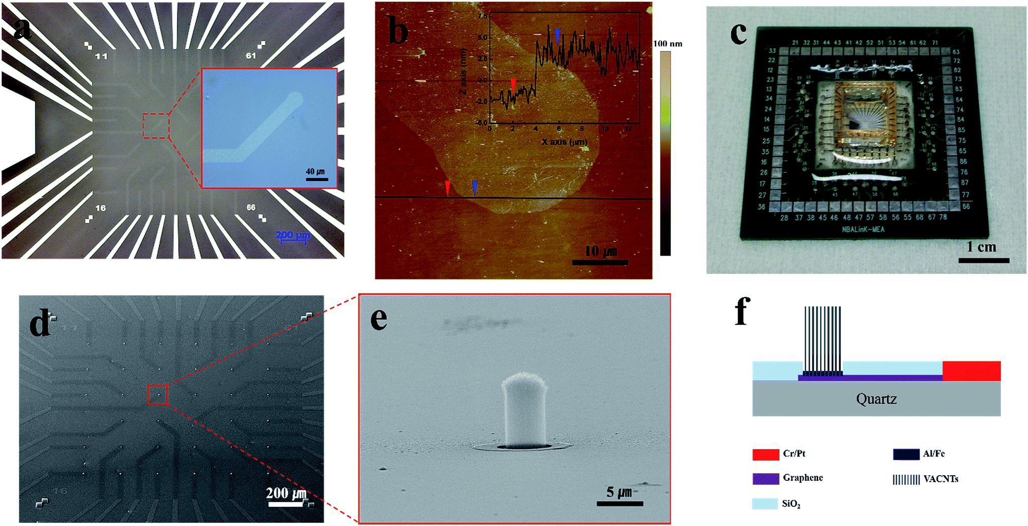 | ||
| Fig. 1 TGVH device used to record neuronal signals. (a) Optical images of a patterned graphene electrode array. Patterned 35-channels graphene electrodes (1 × 1 mm) with an internal ground electrode (2.9 mm2) on a Cr/Pt base electrode (inset: magnification of a single-channel graphene electrode). (b) Topological AFM image of a patterned two-layer graphene electrode (inset: thickness of the black line in (b)). (c) Completed TGVH device. FE-SEM images of (d) the as-grown VACNT multi-electrode array and (e) a single-VACNT electrode. (f) A schematic diagram TGVH device. | ||
The as-grown VACNTs exhibited superhydrophobicity, with a water contact angle of 141°. The VACNT surfaces required functionalization to obtain an effective electrochemical reaction in aqueous solutions. As shown in previous studies,27 a 20 min UV-ozone treatment period induced the formation of carbon–oxygen bonds22 on the VACNT surfaces. Although UV-ozone treatment did not introduce structural deformations into the VACNTs, as shown in Fig. S3(b),† immersing the chip in an aqueous solution (deionized (DI) water for 10 min) produced deformations in the VACNT electrodes. The electrodes shrank, and the otherwise smooth top surfaces of the VACNT electrodes became rough after immersing the chip in an aqueous solution, as shown in Fig. S3(c).† These effects were attributed to the capillary forces generated by the drying process.19,28 The electrodes that underwent such processes (UV-ozone treatment + aqueous solution) maintained their properties up to 40 days in an aqueous solution, as confirmed in previous work,27 indicating that the modified electrodes were electrochemically stable and mechanically robust. Subsequent O2 plasma treatment for 5 min, which was necessary for the PDL coating process, did not produce further deformations, as shown in Fig. S3(d).† Overall, these results indicated that the process used in this work was optimized to enhance the interfacial stability between the electrodes and the cells during attachment.29–31
The electrochemical properties of the TGVH electrodes were characterized in an aqueous solution. Fig. 2(a) shows cyclic voltammogram measured at applied voltages that ranged from −0.4 to 0.6 V, with a scan rate of 20 mV s−1 in PBS (0.01 M phosphate buffer, 0.0027 M potassium chloride, and 0.137 M sodium chloride, pH 7.4) containing 10 mM K3[Fe(CN)6]. Here, the TGVH electrode acted as a working electrode, and Ag/AgCl and a Pt wire were used as the reference and counter electrode, respectively. Typical microelectrode behavior with a sigmoidal voltammogram were observed because convergent diffusion toward the edges of the TGVH electrode became significant,32–34 indicating an improvement in the mass transport rate.
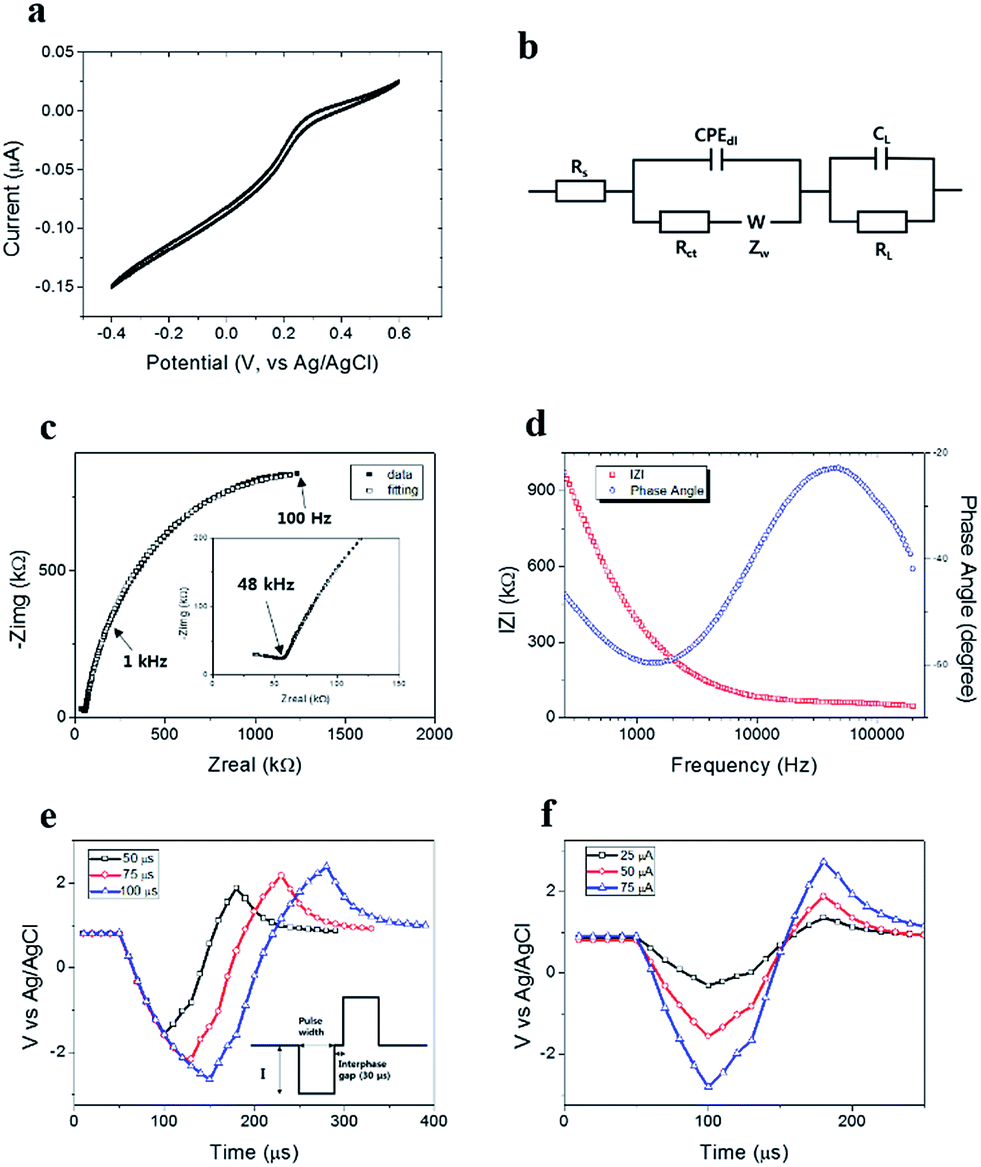 | ||
| Fig. 2 Electrochemical characterization of the TGVH electrode. (a) Cyclic voltammogram of the TGVH electrode at a scan rate 20 mV s−1 in PBS containing 10 mM potassium ferricyanide. (b) Randle's equivalent circuit. (c) Bode plot and (d) Nyquist plot of the impedance spectra obtained from the TGVH electrode, fitted to the equivalent circuit model (b). (e) The charge injection limit varied with (e) the pulse width (50, 75, 100 μs) at a fixed current amplitude (50 μA) (inset: applied biphasic current pulse with an interphase gap (30 μs)) and (f) current amplitudes (25, 50, 75 μA) with a fixed pulse width (50 μs). | ||
Fig. 2(c) presents representative electrochemical impedance spectra (EIS) evaluated at 166 different frequencies ranging from 100 to 200000 Hz in PBS, where the two-electrode measurements collected used the TGVH electrode as a working electrode and the internal ground Pt electrode acted reference and counter electrodes. The equivalent circuit obtained from Randle's model35 (Fig. 2(b)) was used to fit the impedance spectra in Fig. 2(c), where Rs is the equivalent series resistance, CPEdl is the constant phase element of a double layer capacitance, Rct is the charge transfer resistance, ZW is the Warburg element, RL is the leakage resistance, and CL is the mass capacitance (fitted equivalent circuit elements are detailed in Table S1†). The double layer capacitance (Cdl) was calculated as 850 μF cm−2 by fitting to α = 0.8787. Here, the electrode geometry was considered to be a cylinder, with Rs equal to 2.7 kΩ, and Rct equal to 1.5 MΩ. The neural cell signals were effectively recorded using an electrode impedance of 1 kHz (ref. 36–38) because the neural signal frequency is typically on the order of 1 kHz. The impedance value of the TGVH electrode at 1 kHz was 390 kΩ in Fig. 2(d), which was suitable for recoding the neural signals.
The TGVH electrodes with the above-measured properties produced low-noise signal measurements17 and stimulated the neural activity without significant error.39 The charge injection limit of the TGVH electrode was measured using a biphasic current pulse with an interphase gap (30 μs) applied between the TGVH electrode and the Ag/AgCl reference electrode in PBS. Fig. 2(e) and (f) show that the charge injection limit varied with the pulse width and current amplitude, respectively. The capacitive reactions were detected by gradually increasing the pulse width at 50 μA at a fixed current amplitude, as shown in Fig. 2(e). The capacitance extracted from the linear region of the negative current in Fig. 2(f) was estimated to be approximately 776 μF cm−2, comparable to the double layer capacitance obtained from the EIS measurement.
Spontaneous action potentials may be recorded by culturing cortex neurons dissociated from embryos of an embryonic day 17 SD rat on the VACNTs electrodes coated with PDL to enhance cellular adhesion to the surface. Fig. S4† shows optical images of the cultured neural cells on the TGVH device as a function of DIV. During all stages of development, cells formed stable adhesions to the substrate, and a homogeneous distribution of cortical neuronal cell bodies and neurites was clearly observed through the transparent TGVH devices. A tangled neuronal network developed beyond 6 DIV, and this network remained healthy for one month, suggesting biocompatibility with the TGVH electrode. The cultured cortical neurons were closely investigated after 6 DIV, in accordance with the electrophysiological characteristics and the synaptic connections.40,41 The spontaneous electrical signals of the cortex neurons cultured on the TGVH device were measured using a Home-built MEA System with a 20 kHz sampling rate based on LabVIEW software (National Instruments).42,43 All recorded signals were filtered through a band pass filter with a 300–3000 Hz window, followed by a notch filter to remove 60 Hz noise (as described in the ESI Fig. S5†). Extracellular action potentials with a high amplitude, as shown in Fig. S6,† were reliably recorded from cortical neurons over nearly one month (Fig. S7 and S8†).
The neurons cultured on the TGVH device at 7 DIV were identified by immunofluorescence staining (Fig. 3(a)), which revealed the presence of healthy synaptic connections. The outstanding adhesion between the VACNTs and the axons or dendrites of the neurons is displayed in Fig. 3(b) and (c) and was attributed to the three-dimensional VACNTs electrode with a modified nano-surface.20,21 As shown by Xie et al., mesoscale secondary features on a cellular substrate can enhance cell attachment, growth, and cellular activity.19 A robust interface produces a maximum peak-to-peak amplitude of approximately 1.6 mV with a root mean square (RMS) noise level of 5.92 μV (E29 in Fig. S7†), where the estimated SNR is approximately 215 (considering the negative amplitude spike). The high-amplitude negative spike with a peak amplitude of nearly 1 mV was thought to originate from the action potential of the adjacent soma of a neuron.44 Such a high signal amplitude is seldom observed using extracellular signal measurements that do not involve electroporation, confirming the excellent performances of the TGVH electrodes. The various extracellular action potential waveforms were associated with the position of the attached cell segment on the recording electrode and the distance between the electrode and the cell.45 Partial burst firing activities characteristic of activation patterns of neurons in the central nervous system46,47 were also detected, as shown in Fig. S8(b).†
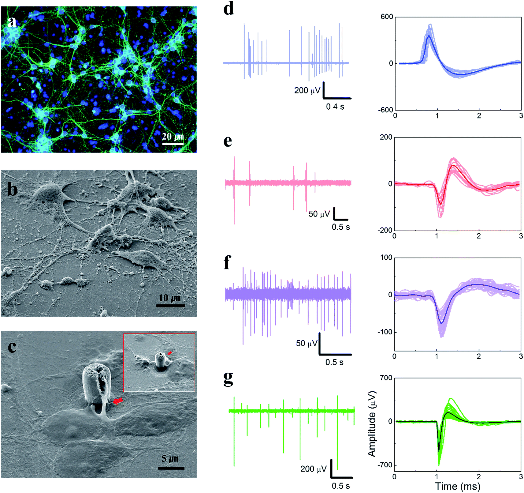 | ||
| Fig. 3 The rat cortical neurons on a TGVH device, and a variety of recorded spike waveforms. (a) Representative merged fluorescence images of rat cortical neurons at 7 DIV. Here, the blue and green correspond to the nucleus and membrane, respectively. (b) and (c) show FE-SEM images of the fixed rat cortical neuron cultured on a TGVH device at 7 DIV (inset: another degree view of (c), the red arrows indicate the cell membranes), after deposition of the Pt (15 nm) layer. The representative recorded signals exhibit various spike waveforms, as shown in (d)–(g). | ||
Fig. 3(d) exhibits a positive spike waveform derived from a distal soma, such as a dendritic compartment, due to the positive capacitive current as a result of current conservation.44,47 Biphasic spike waveforms with an average peak-to-peak amplitude of −168 μV were recorded, as shown in Fig. 3(e). These waveforms are often detected in cultured neuronal cells in our system using other electrodes.42,43 These waveforms may correspond to a positive capacitive current.44,47 The negative spiked waveforms (Fig. 3(f) and (g)) originated from the vicinity of a soma of neuron, with an amplitude that depended on the distance between the electrode and the cell.45 The observed diverse spiked waveforms demonstrated that the TGVH electrodes formed close contact with the substructures of the neuronal cells, such as the somas, axons, and dendrites. Furthermore, assuming that the number of spikes was closely related to the number of cells having a firing activity, wherein each cell was considered to be a point source, the distance-dependence spike amplitude was found to follow a particular distribution. ESI Fig. S9† presents a stochastic model distribution of the distance-dependent spike amplitude deduced from the number of detected spikes and the average amplitude. The spike amplitude decreases with increasing distance from the soma;45,47–49 therefore, the neuronal activities could be analyzed using a stochastic model system.
The TGVH was assessed by investigating the performances of the TGVH electrode and a smooth commercial TiN electrode 30 μm in diameter. Measurements were performed after 3 weeks of cell culture, because mature neuronal cells fire high-frequency and high-amplitude action potentials.50 Fig. 4(a) plots representative signals recorded using the TGVH electrodes, revealing a remarkably high signal amplitude compared to the commercial electrode. The noise floors of the two systems were similar. The maximum SNR of the TGVH electrode (287) was 5 times that of the TiN electrode (54.95), as shown in Fig. 4(b), with a similar RMS noise (TGVH electrode: 3.502 μV, commercial electrode: 3.528 μV). Although we did not expect that the TGVH electrode was completely engulfed by the cell, a large SNR was observed, similar to the results obtained from a mushroom-shaped electrode.51 Therefore, we assumed that the TGVH electrode induced strong coupling between the electrode and the cell, possibly due to the three-dimensional VACNT electrode with a shrunken and crinkly surface, as shown in Fig. S3.† Fig. 4(c) and (d) show that the spikes recorded from 3 representative TGVH electrodes spanned a wide range of negative values, from −30 to −1275 μV, whereas those recorded from the TiN electrodes fell within the range −30 to −200 μV. As with the carbon nanotube electrodes interfaced with retinal tissue,16 the number of detected spikes was lager when using the TiN electrodes, whereas the TGVH electrodes showed signals with a higher amplitude. The difference in the number of spike events was mainly attributed to the electrode size, whereas the amplitude distribution depended on the electrode–cell coupling. The diameter of the active TGVH electrode was 5 μm; therefore, it was unlikely that the electrode was coupled to more than one cell, although one cannot completely rule out the possibility of signal superposition from a nearby neuron cell. Both electrodes exhibited similar distributions of spike amplitudes, with TGVH showing slightly larger distributions.
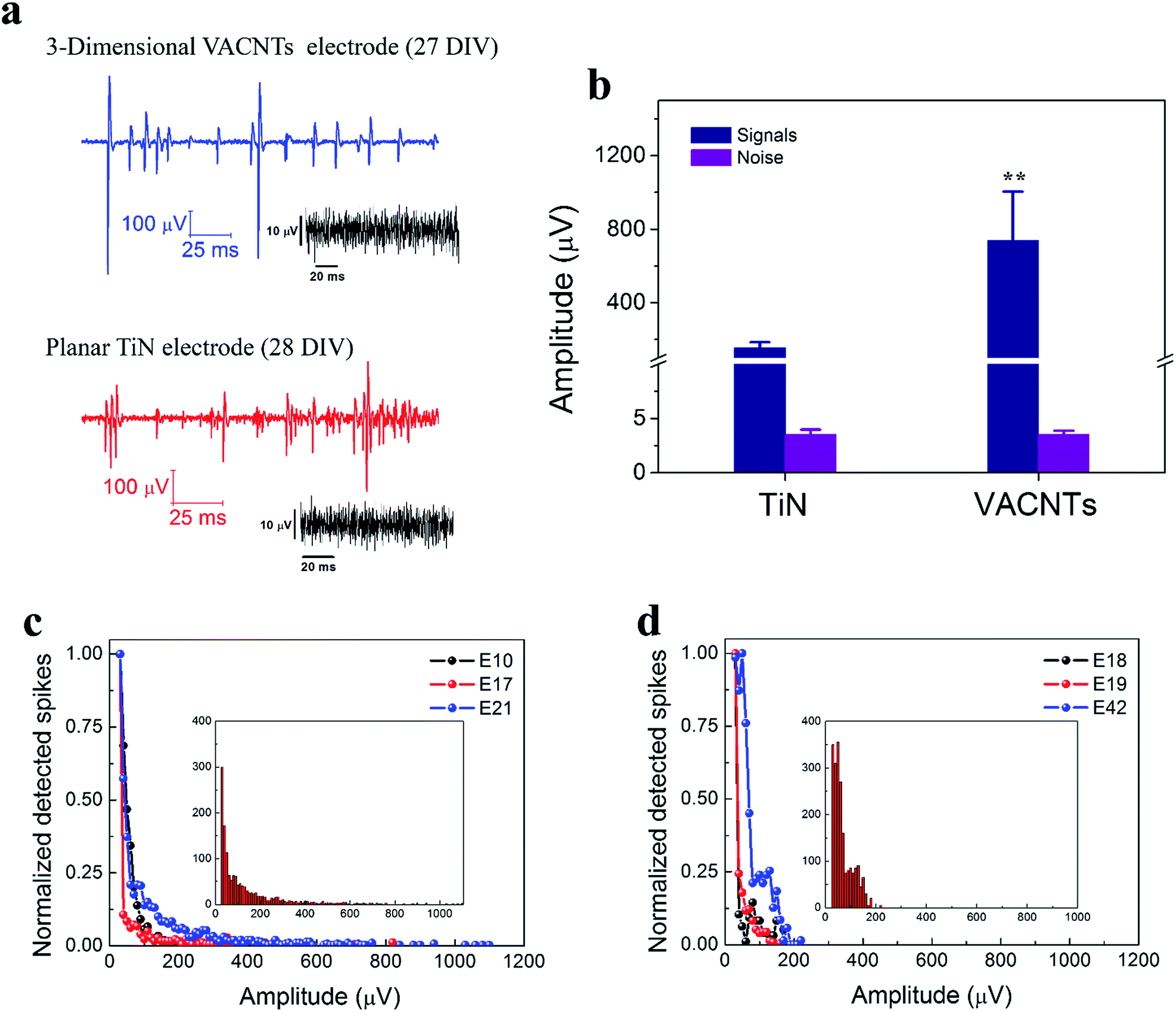 | ||
| Fig. 4 Signals recorded from the three-dimensional VACNT electrodes with a modified nanoscale surface, as compared with the signals recorded from the smooth commercial electrode. (a) The signals of a representative VACNTs electrode (diameter: 5 μm, height: 7–10 μm) and a smooth commercial electrode (TiN, diameter: 30 μm) were recorded at 27 DIV and 28 DIV, respectively. (b) The maximum spike amplitude of the VACNT electrode (n = 5) was approximately 1.2 mV, whereas the corresponding value obtained from the commercial electrode (n = 5), by contrast, was barely 218 μV. The normalized spikes detected in using the (c) VACNTs electrode and (d) the smooth TiN electrode as a function of the amplitude (inset: number of detected spikes versus the spike amplitude). ** P < 0.01. | ||
The cause of the enhanced signal amplitude measured using the TGVH electrodes was explored using transmission electron microscopy (TEM) analysis of the interface in Fig. 5 and S10.† Fig. 5(a) shows a cross-sectional SEM image of a cortical neuron cultured on a TGVH electrode at 7 DIV. As shown in Fig. 5(b) and (c), no cleft formed between the VACNTs with an average tube diameter of 10–20 nm,23 and the cell membrane ensured that the cultured neurons closely adhered to the VACNT surfaces.52 The tight adhesion led to a high seal resistance associated with a high SNR.53 We could not expect the cells to engulf the VACNTs, as in the case of sub-micron electrodes;9,18,54 therefore, we considered the contact area ratio between the electrode (Fig. S11†) and the cell (as described in detail in the ESI†). In our model, the seal resistance used for the simulation was estimated to exceed 50 MΩ, considering that the three-dimensional structure produced a narrow partial cleft (<10 nm).9,51,53,54 This value is comparable with that of capped, high-aspect ratio nanoscale cylinder extensively investigated in the recent work of Santoro et al.55 The equivalent circuit (Fig. 5(d)) predicted the expected amplitude of the extracellular action potential, which depended on the seal resistance and the contact area ratio, as shown in Fig. 5(e). The shape and amplitude of the simulated spike corresponded well to the average extracellular action potential recorded using the TGVH electrode (Fig. S12†), as shown in Fig. 5(f).
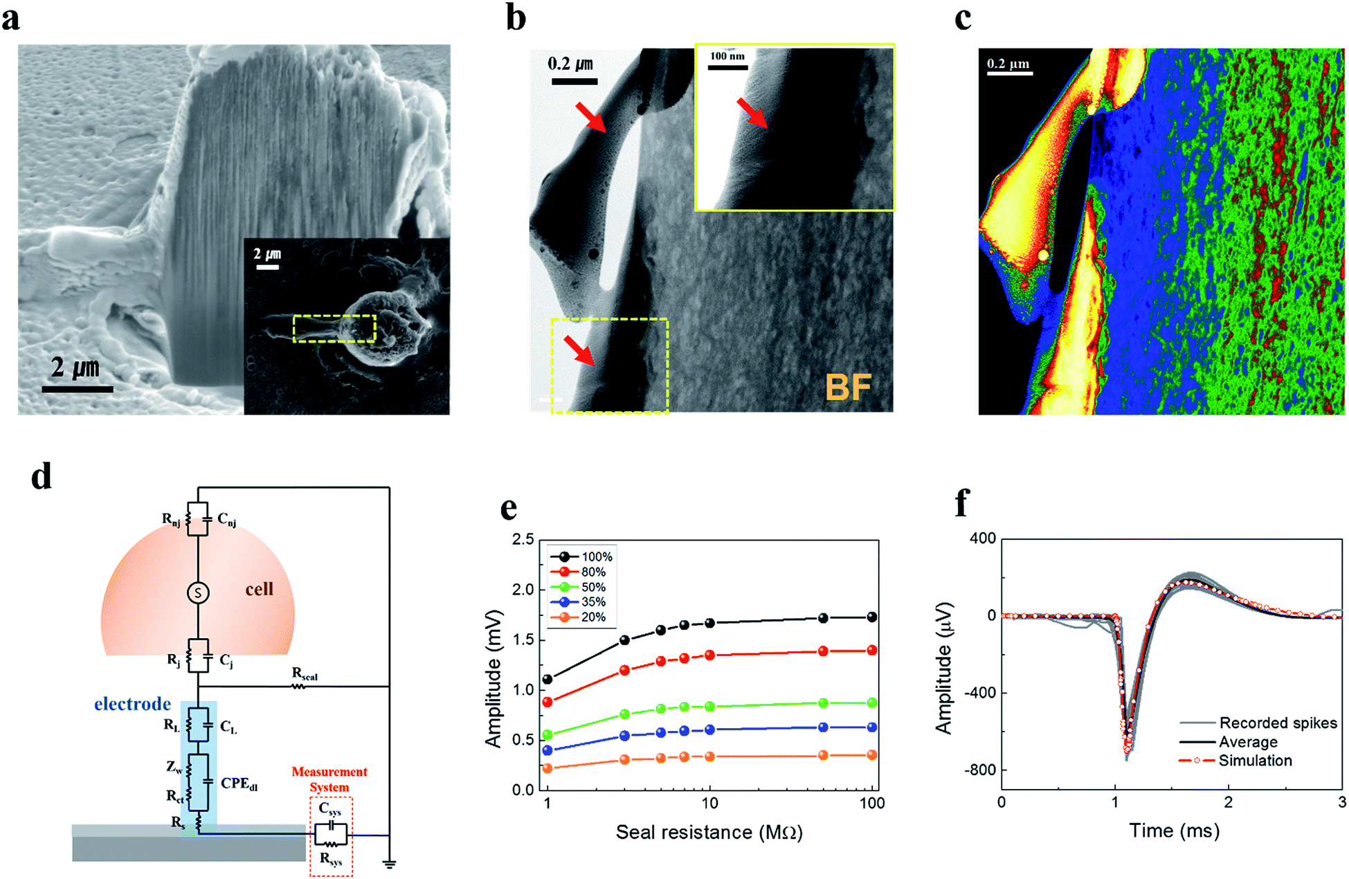 | ||
| Fig. 5 Simulation of the amplitude expected from the extracellular action potential as a function of the seal resistance and coupling coefficient, based on the TEM images. (a) The cross-sectional SEM image of a cortical neuron on a VACNT electrode after fixation (inset: top view). (b) Bright-Field (BF) TEM images of the interface between a neuron and a VACNT electrode in the area marked in (a) (inset: high-magnification view of the yellow area marked in (b). The red arrows indicate the neuron membrane). (c) High-angle annular dark-field (HAADF) image and corresponding energy dispersive spectrometry (EDS) (as described in detail in the ESI Fig. S10†) results revealed the intensive accumulation of Ga ions on the remaining cell during the cross-sectioning process. (d) Equivalent circuit of the interface between the cortical neuron and the VACNT electrode (as described in detail in the ESI†). (e) The expected amplitudes of the recorded extracellular action potential, simulated as a function of the seal resistance and the contact area ratio between the neuron and the VACNT electrode (as described in detail in the ESI S11 and S12†). (f) The simulated spike (red line), assuming a 35% contact area ratio and a 50 MΩ seal resistance, corresponded closely to the average amplitude (black line) of the recorded spikes (gray line). | ||
Conclusion
TGVH electrodes were developed to facilitate the optical monitoring of cells and the simultaneous recording of extracellular signals. Spontaneous action potentials from cortical neurons measured using TGVH electrodes exhibited an exceptionally high signal amplitude and SNR. High signal amplitudes are characteristic of CNTs, given the porosity of the CNT network, the suitability of the surface properties for cell adhesion and proliferation, and the electrical conductivity of the CNTs. VACNTs in TGVH electrodes provide a protruded geometry that is suitable for cell interfaces. Post-fabrication treatments formed nanoscale structures that favored cell attachment and growth. The TGVH electrodes exhibited a high capacitance and a high charge injection limit, which lowered the noise levels and decreased the impedance. The recorded signals, which had a variety of spike waveforms, revealed that three-dimensional VACNT electrodes with nanostructured surfaces favorably interfaced with all segments of a cortical neuron cell. The modified structures provided a high SNR (287) due to excellent cell adhesion, 5 times the cell adhesion obtained using the commercial TiN electrode. The TGVH electrodes may enable minimally invasive, sensitive cellular signal measurements over prolonged periods of time while permitting optical monitoring or control at the same time. These advantages of the TGVH electrodes may be useful in basic science research geared toward understanding brain function, as well as in electrode engineering applications for electrocorticography. Remaining issues that must be addressed prior to the development of practical applications of TGVH electrodes include: increasing the device yield and construction on flexible substrates to form conformal contact with brain tissue. Although these limitations are still being addressed, TGVH electrodes provide a useful tool for drug screening, toxicity assessments, and measurements of signal transfer in cells.Acknowledgements
This research was supported by the Creative Fusion Research Program through the Creative Allied Project funded by the National Research Council of Science & Technology (CAP-12-1-KIST), the Electronics & Telecommunications Research Institute (project 16ZH1210), and by the 2015 Research Fund (1.150114.01) of UNIST(Ulsan National Institute of Science & Technology). Authors also acknowledge the assistance of Professor Min Sun Kim at Wonkwang University Hospital in extracting primary neuronal cells.References
- L. R. Hochberg, M. D. Serruya, G. M. Friehs, J. A. Mukand, M. Saleh, A. H. Caplan, A. Branner, D. Chen, R. D. Penn and J. P. Donoghue, Nature, 2006, 442, 164–171 CrossRef CAS PubMed.
- C. E. Bouton, A. Shaikhouni, N. V. Annetta, M. A. Bockbrader, D. A. Friedenber, D. M. Nielson, G. Sharma, P. B. Sederber, B. C. Glenn, W. J. Mysiw, A. G. Morgan, M. Deogaonkar and A. R. Rezai, Nature, 2016, 533, 247–250 CrossRef CAS PubMed.
- T. J. Oxley, N. L. Opie, S. E. John, G. S. Rind, S. M. Ronayne, T. L. Wheeler, J. W. Judy, A. J. McDonald, A. Dornom, T. J. H. Lovell, C. Steward, D. J. Garrett, B. A. Moffat, E. H. Lui, N. Yassi, B. C. V. Campbell, Y. T. Wong, K. E. Fox, E. S. Nurse, I. E. Bennett, S. H. Bauquier, K. A. Liyanage, N. R. Nagel, P. Perucca, A. Ahnood, K. P. Gill, B. Yan, L. Churilov, C. R. French, P. M. Desmond, M. K. Horne, L. Kiers, S. Prawer, S. M. Davis, A. N. Burkitt, P. J. Mitchell, D. B. Grayden, C. N. May and T. J. O'Brien, Nat. Biotechnol., 2016, 34, 320–327 CrossRef CAS PubMed.
- K. J. Yu, D. Kuzum, S.-W. Hwang, B. H. Kim, H. Juul, N. H. Kim, S. M Won, K. Chiang, M. Trumpis, A. G. Richardson, H. Cheng, H. Fang, M. Thompson, H. Bink, D. Talos, K. J. Seo, H. N. Lee, S.-K. Kang, J.-H. Kim, J. Y. Lee, Y. Huang, F. E. Jensen, M. A. Dichter, T. H. Lucas, J. Viventi, B. Litt and J. A. Rogers, Nat. Mater., 2016, 15, 782–791 CrossRef CAS PubMed.
- M. Heim, L. Rousseau, L. Reculusa, V. Urbanova, S. J. Mazzocco, L. Bouffier, K. Vytras, P. Bartlett, A. Kuhn and B. Yvert, J. Neurophysiol., 2012, 108, 1793–1803 CrossRef PubMed.
- S. F. Cogan, Annu. Rev. Biomed. Eng., 2008, 10, 275–309 CrossRef CAS PubMed.
- E. W. Keefer, B. R. Botterman, M. I. Romero, A. F. Rossi and G. W. Gross, Nat. Nanotechnol., 2008, 3, 434–439 CrossRef CAS PubMed.
- C. Xie, Z. Lin, L. Hanson, Y. Cui and B. Cui, Nat. Nanotechnol., 2012, 7, 185–190 CrossRef CAS PubMed.
- A. Hai, J. Shappir and M. E. Spira, J. Neurophysiol., 2010, 104, 559–568 CrossRef CAS PubMed.
- T. Dvir, B. P. Timko, D. S. Kohane and R. Langer, Nat. Nanotechnol., 2011, 6, 13–22 CrossRef CAS PubMed.
- B. Tian, J. Liu, L. Jin, J. H. Tsui, Q. Qing, Z. Suo, R. Langer, D. S. Kohane and C. M. Lieber, Nat. Mater., 2012, 11, 986–994 CrossRef CAS PubMed.
- J. Liu, T.-M. Fu, Z. Cheng, G. Hong, T. Zhou, L. Jin, M. Durruri, Z. Jing, P. Kruskal, C. Xie, Z. Suo, Y. Fang and C. M. Lieber, Nat. Nanotechnol., 2015, 10, 629–636 CrossRef CAS PubMed.
- J. T. Robinson, M. Jorgolli, A. K. Shalek, M.-H. Yoon, R. S. Gertner and H. Park, Nat. Nanotechnol., 2012, 7, 180–184 CrossRef CAS PubMed.
- B. Tian, T. Cohen–Karni, Q. Qing, X. Duan, P. Xie and C. M. Lieber, Science, 2010, 329, 830–834 CrossRef CAS PubMed.
- X. Duan, R. Gao, P. Xie, T. Cohen-Karni, Q. Qing, H. S. Choe, B. Tian, X. Jing and C. M. Lieber, Nat. Nanotechnol., 2012, 7, 174–179 CrossRef CAS PubMed.
- A. Shoval, C. Adams, M. David–Pur, M. Shein, Y. Hanein and E. Sernagor, Front. Neuroeng., 2009, 2, 1–8 Search PubMed.
- L. Bareket-Keren and Y. Hanein, Front. Neural Circuits, 2013, 6, 1–16 Search PubMed.
- Z. C. Lin, C. Xie, Y. Osakada, Y. Cui and B. Cui, Nat. Commun., 2014, 5, 3206 Search PubMed.
- X. Xie, W. Zhao, H. R. Lee, C. Liu, M. Ye, W. Xie, B. Cui, C. S. Criddle and Y. Cui, ACS Nano, 2014, 8, 11958–11965 CrossRef CAS PubMed.
- T. Limongi, F. Cesca, F. Gentile, R. Marotta, R. Ruffilli, A. Barberis, M. D. Maschio, E. M. Petrini, S. Santoriello, F. Benfenati and E. D. Fabrizio, Small, 2013, 9, 402–412 CrossRef CAS PubMed.
- M. Li, N. Hakimi, R. Perez, S. Waldman, J. A. Kozinski and D. K. Hwang, Adv. Mater., 2015, 27, 1880–1886 CrossRef CAS PubMed.
- B.-L. Hsu, I.-J. Teng, Y.-C. Chen, W.-L. Hsu, Y.-T. Lee, S.-J. Yen, H.-C. Su, S.-R. Yeh, H. Chen and T.-R. Yew, Adv. Mater., 2010, 22, 2177–2181 CrossRef PubMed.
- S. Park, D.-W. Park, C.-S. Yang, K.-R. Kim, J.-H. Kwak, H.-M. So, C. W. Ahn, B. S. Kim, H. Chang and J.-O. Lee, ACS Nano, 2011, 9, 7061–7068 CrossRef PubMed.
- D.-W. Park, A. A. Schendel, S. Mikael, S. K. Brodnick, T. J. Richner, J. P. Ness, M. R. Hayat, F. Atry, S. T. Frey, R. Pashaie, S. Thongpang, Z. Ma and J. C. Williams, Nat. Commun., 2014, 5, 5258 CrossRef CAS PubMed.
- D. Kuzum, H. Takano, E. Shim, J. C. Reed, H. Juul, A. G. Richardson, J. D. Vries, H. Bink, M. A. Dichter, T. H. Lucas, D. A. Coulter, E. Cubukcu and B. Litt, Nat. Commun., 2014, 5, 5259 CrossRef CAS PubMed.
- Y. Zhu, L. Li, C. Zhang, G. Casillas, Z. Sun, Z. Yan, G. Ruan, Z. Peng, A.-R. O. Raji, C. Kittrell, R. H. Hauge and J. M. Tour, Nat. Commun., 2012, 3, 1225 CrossRef PubMed.
- D. W. Jeong, J. Jung, G. H. Kim, C.-S. Yang, J. J. Kim, S. D. Jung and J.-O. Lee, Nanotechnology, 2015, 26, 335701 CrossRef PubMed.
- N. Chakrapani, B. Wei, A. Carrillo, P. M. Ajayan and R. S. Kane, Proc. Natl. Acad. Sci. U. S. A., 2004, 101, 4009–4012 CrossRef CAS PubMed.
- X. Zhang, S. Prasad, S. Niyogi, A. Morgan, M. Ozkan and C. S. Ozkan, Sens. Actuators, B, 2005, 106, 843–850 CrossRef CAS.
- E. García-Fruitós, J. Seras-Franzoso, E. Vazquez and A. Villaverde, Nanotechnology, 2010, 21, 205101 CrossRef PubMed.
- G. Cellot, F. M. Toma, Z. K. Varley, J. Laishram, A. Villari, M. Quintana, S. Cipollone, M. Prato and L. Ballerini, J. Neurosci., 2011, 7, 12945–12953 CrossRef PubMed.
- N. Punbusayakul, L. Ci, S. Talapatra, W. Surareungchai and P. M. Ajayan, J. Nanosci. Nanotechnol., 2007, 8, 1–6 Search PubMed.
- D. A. Walsh, K. R. J. Lovelock and P. Licence, Chem. Soc. Rev., 2010, 38, 4185–4194 RSC.
- D. W. M. Arrigan, Analyst, 2004, 129, 1157–1165 RSC.
- W. Wang, S. Guo, I. Lee, K. Ahmed, J. Zhong, Z. Favors, F. Zaera, M. Ozkan and C. S. Ozkan, Sci. Rep., 2014, 4, 4452 Search PubMed.
- J. C. Williams, J. A. Hippensteel, J. Dilgen, W. Shain and D. R. Kipke, J. Neural Eng., 2007, 4, 410–423 CrossRef PubMed.
- P. Norlin, M. Kindlundh, A. Mouroux, K. Yoshida and U. G. Hofmann, J. Micromech. Microeng., 2002, 12, 414–419 CrossRef CAS.
- B. J. Kim, J. T. W. Kuo, S. A. Kuo, C. D. Lee, L. Yu, C. A. Gutierrez, T. Q. Hoang, V. Pikov and E. Meng, J. Neural Eng., 2013, 10, 045002 CrossRef CAS PubMed.
- C. R. Butson and C. C. McIntyre, Clin. Neurophysiol., 2005, 116, 2490–2500 CrossRef PubMed.
- M. A. Dichter, Brain Res., 1978, 149, 279–293 CrossRef CAS PubMed.
- H. J. Romijn, M. T. Mud, A. M. Habets and P. S. Wolters, Brain Res., 1981, 227, 591–605 CrossRef CAS PubMed.
- Y. H. Kim, G. H. Kim, A. Y. Kim, Y. H. Han, M.-A. Chung and S.-D. Jung, J. Neural Eng., 2015, 12, 066029 CrossRef PubMed.
- Y. H. Kim, G. H. Kim, A.-Y. Kim, N. S. Beak, J. I. Jeong, Y. H. Han, B. C. Shin, M.-A. Chung and S.-D. Jung, RSC Adv., 2015, 5, 6675–6681 RSC.
- C. Gold, C. C. Girardin, K. A. C. Martin and C. Koch, J. Neurophysiol., 2009, 102, 3340–3351 CrossRef PubMed.
- G. Buzsáki, C. A. Anastassiou and C. Koch, Nat. Rev. Neurosci., 2012, 13, 407–420 CrossRef PubMed.
- D. C. Cooper, Neurochem. Int., 2002, 41, 333–340 CrossRef CAS PubMed.
- C. Gold, D. A. Henze, C. Koch and G. Buzsáki, J. Neurophysiol., 2006, 95, 3113–3128 CrossRef CAS PubMed.
- D. A. Henze, Z. Borhegyi, J. Csicsvari, A. Mamiya, K. D. Harris and G. Buzsáki, J. Neurophysiol., 2000, 84, 390–400 CAS.
- G. Buzsáki, Nat. Neurosci., 2004, 7, 446–451 CrossRef PubMed.
- Z.-W. Zhang, J. Neurophysiol., 2004, 91, 1171–1182 CrossRef PubMed.
- A. Hai, A. Dormann, J. Shappir, S. Yitzchaik, C. Bartic, G. Borghs, J. P. M. Langedijk and M. E. Spira, J. R. Soc., Interface, 2009, 6, 1153–1165 CrossRef CAS PubMed.
- G. Cellot, E. Cilia, S. Cipollone, V. Rancic, A. Sucapane, S. Giordani, L. Gambazzi, H. Markram, M. Gandolfo, D. Scaini, F. Gelain, L. Casalis, M. Prato, M. Giugliano and L. Ballerini, Nat. Nanotechnol., 2009, 4, 126–133 CrossRef CAS PubMed.
- M. E. Spira and A. Hai, Nat. Nanotechnol., 2013, 8, 83–94 CrossRef CAS PubMed.
- S. M. Ojovan, N. Rabieh, N. Shmoel, H. Erez, E. Maydan, A. Cohen and M. E. Spira, Sci. Rep., 2015, 5, 14100 CrossRef CAS PubMed.
- F. Santoro, S. Dasgupta, J. Schnitker, T. Auth, E. Neumann, G. Panitov, G. Gompper and A. Offenhäusser, ACS Nano, 2014, 8, 6713–6723 CrossRef CAS PubMed.
Footnotes |
| † Electronic supplementary information (ESI) available: Raman spectra of graphene electrodes, device fabrication scheme of TGVH device, SEM images that show deformation of VACNT electrodes, optical images of cortical neurons cultured on TGVH device, Home-built MEA systems for recording neuronal signals, action potentials recorded by TGVH electrodes 6–28 DIV, enlarged spontaneous action potential peaks from 3 electrodes at 7 DIV, burst firing activity of the neuron cells, the distance dependence of the spike amplitude, TEM analysis of the interface between VACNT electrodes and the cell, simulation details of extracellular action potential and schematics of neuronal cell-VACNT interfaces. See DOI: 10.1039/c6ra26836f |
| ‡ These authors contributed equally to this work. |
| This journal is © The Royal Society of Chemistry 2017 |